Note : Les descriptions sont présentées dans la langue officielle dans laquelle elles ont été soumises.
~~ O 95110107 ~ 1 l 2 5 5 2 pCT/US94110871
ELECTROPHORETIC DISPLAY PANEL WITH
SELECTIVE CHARACTER ADDRESSABILITY
BACKGROUND ART
$ This invention relates to electrophoretic display devices in
general and, more particularly, to an electrophoretic display apparatus which
employs means for selectively erasing and rewriting individual characters on
the
display panel thereof.
Electrophoretic displays (EPIDS) are now well known. A variety
of display types and features are taught in several patents issued in the
names
of the inventors herein, Frank J. DiSanto and Denis A. Krusos and assigned to
the assignee herein, Copytele, Inc. of Huntington Station, New York. For
example, U.S. Patent Nos. 4,655,897 and 4,732,830, each entitled
ELECTROPHORETIC DISPLAY PANELS AND ASSOCIATED METHODS
describe the basic operation and construction of an electrophoretic display.
U.S. Patent No. 4,742,345, entitled ELECTROPHORETIC DISPLAY PANELS
AND METHODS THEREFOR, describes a display having improved alignment
and contrast. Many other patents regarding such displays are also assigned to
Copytele, Inc.
The display panels shown in the above-mentioned patents operate
upon the same basic principle, viz., if a suspension of electrically charged
pigment particles in a dielectric fluid is subjected to an applied
electrostatic
field, the pigment particles will migrate through the fluid in response to the
electrostatic field. Given a substantially homogeneous suspension of particles
having a pigment color different from that of the dielectric fluid, if the
applied
electrostatic field is localized it will cause a visually observable localized
pigment particle migration. The localized pigment particle migration results
either in a localized area of concentration or rarefaction of particles
depending
WO 95/10107 217 2 5 5 2 PCT~S94/10871
2
upon the polarity and direction of the electrostatic field and the charge on
the
pigment particles.
The electrophoretic display apparatus taught in the foregoing
U.S. Patents are "triode-type" displays having a plurality of parallel cathode
lines and a plurality of transverse grid electrode lines insulated from the
cathode lines. The cathode and grid lines are referred to as row and columns
and the terms may be interchanged. The grid cathode structure forms an X-Y
matrix enabling one to address the display at each X-Y intersection and
thereby cause pigment particles to migrate relative to the cathode. Given a
specific particulate suspension, the sign of the electrostatic charge which
will
attract and repel the pigment particles will be known. The cathode voltage,
the
anode voltage, and the grid element voltage can then be ascertained such that
when a particular voltage is applied to the cathode and another voltage is
applied to the grid, the area proximate their intersection will assume a net
charge sufficient to attract or repel pigment particles in suspension in the
dielectric fluid.
Since numerous cathode and grid lines are employed, there are
numerous discrete intersection points which can be controlled by varying the
voltage on the cathode and grid elements to cause localized visible regions of
pigment concentration and rarefaction. Essentially then, the operating
voltages
on both cathode and grid must be able to assume at least two states
corresponding to a logical one and a logical zero. Logical one for the cathode
may either correspond to attraction or repulsion of pigment. Typically, the
cathode and grid voltages are selected such that only when both are a logical
one at a particular intersection point, will a sufficient electrostatic field
be
present at the intersection relative to the anode to cause the writing of a
visual
bit of information on the display through migration of pigment particles. The
bit may be erased, e.g., upon a reversal of polarity and a logical zero-zero
state
....CVO 95/10107 PCT/I1S94110871
212552
3
occurring at the intersection coordinated with an erase voltage gradient
between anode and cathode. In this manner, digitized data can be displayed
on the electrophoretic display.
Accordingly, in order to erase the image in an electrophoretic
. 5 display of the type in which negatively charged, light colored pigment
particles
are suspended in a dark-colored suspension medium, the anode is biased
negatively relative to the cathode so that the particles are attracted to the
cathode. In the aforementioned type of electrophoretic display device, the
anode is typically a thin, unitary layer of ITO to which a first voltage is
applied
in the write mode and a different voltage is applied in an erase mode. All
lines of the displayed image are erased simultaneously upon application of the
erase voltage anode, and all lines of the display must be rewritten to form
the
next image frame. The next frame may often have character lines for image
portions which are the same as the previous frame, which results in the
redundancy of rewriting numerous identical lines from frame to frame.
There are also anode electrode structures which comprise
conductor strips instead of a solid thin layer of ITO. One such anode
structure
is described in U.S. Patent Number 5,053,763, issued to Frank J. DiSanto and
Denis A. Krusos, entitled DUAL ANODE FLAT PANEL ELECTROPHORETIC
DISPLAY, which is also owned by the assignee of the present application. In
an electrophoretic display panel which is used to display text, characters are
formed utilizing a predetermined number of such anode conductor strips in a
group, the predetermined number of anode conductor strips being referred to
as a character line and each of the predetermined number of anode conductor
strips in the character line being referred to as an anode line segment. For
example, in a typical such electrophoretic display panel, a character line is
comprised of 26 anode line segments, each of which is approximately 0.125"
wide and each of which is spaced approximately .001" from adjacent segments.
WO 95/10107 ~ .-
21.7 2 5 5 2 PCT/US94/10871
4
A "selective" erase operation of a multiplicity of character lines, each of
which
comprises a multiplicity of anode line segments, is performed by applying a
negative voltage to the anode line segments of the selected character lines.
While the segmented anode structure described above permits a
frame to be written much faster than previous display devices, the selective
erase operation it performs is not equally effective in all situations. For
example, where only a few characters of a single line are to be erased or
rewritten and a negative voltage is applied to the anode line segments of the
selected character line, a part of adjacent character lines on either side of
the
selected character line are also erased. As such, the display can temporarily
appear illegible or hard to read. Moreover, the erasure of an entire line is
time consuming and inefficient when only a few characters or less of a
character line are to be erased or rewritten.
In U.S. Pat. No. 5,174,882, entitled ELECTRODE STRUCTURE
FOR AN ELECTROPHORETIC DISPLAY APPARATUS and issued on Dec.
29, 1992 to Frank J. DiSanto and Denis A. Krusos, there is illustrated another
display device which includes a segmented anode structure. This patent
prevents the partial erasure of adjacent character lines by configuring the
anode as a plurality of alternating conductors. When selected for erasure of a
corresponding character line, one of the conductors is biased with an erase
potential of a given polarity and adjacent conductors are biased with a
potential of an opposite polarity. The latter conductors prevent the partial
erasure of the adjacent character lines. As in the case of the '763 device,
however, the operation of this device also requires the erasure and rewriting
of
all characters of a selected line, which erasure is time consuming and
inefficient when only a few characters need be erased or rewritten.
Accordingly, it is an object of the present invention to provide a
method and an electrophoretic display which overcomes the aforementioned
.-:CVO 95/10107 217 2 5 5 2 pCT~S94/10871
disadvantages of the prior art devices. In particular, the object of the
invention
is to provide an electrophoretic display in which individual characters on a
line
of the display can be selectively erased and rewritten without materially
disturbing the appearance of other image characters of that line which remain
$ the same from one frame to the next.
DISCLOSURE OF THE INVENTION
Pursuant to this object, and others which will become apparent
hereafter, an electrophoretic display apparatus comprises a panel having a
display surface and containing an electrophoretic dispersion of particles in a
suspension medium, writing means for forming a plurality of image lines on the
display surface in a write mode by either attracting charged particles from
the
dispersion onto the display surface or repelling the same therefrom, and
selective character erasing means adapted to rapidly erase a single character
of
1$ a character line without materially affecting the legibility of adjacent
characters
thereof.
In one embodiment of the invention, the display surface is the
cathode of the electrophoretic display and the selective character erasing
means comprises a multiplicity of anode line segments, wherein each character
line of the display is defined by at least one of the anode segments and by a
corresponding group of row and column electrode intersections. The display
further includes control means operable in a partial erase mode to apply a
first
potential bias of a given polarity between an anode segment corresponding to a
selected character line containing a character to be erased and a
corresponding
2$ group of row and column intersections long enough to cause pigment
particles
to move relative to the intersections and to thereby partially erase the
selected
character line. The control means are operable in a second mode to apply a
second potential bias of an opposite polarity between the anode segment and
2 ~ ~ 2 5 5 2 PCT/US94/10871
WO 95/10107
6
the group of row and column intersections for a period of time sufficient to
partially rewrite characters of the character line not selected for erasure,
and
the control means is operable to alternately apply the first and second
potential
biases until the character to be erased is no longer displayed.
A method for selectively erasing a character of a character line
comprises the steps of partially erasing a character line having a character
thereof selected for erasure, rewriting to the character line all characters
not
selected for erasure, and repeating the partial erasure and rewriting steps
sequentially until the selected character is no longer visible on said
display.
BRIEF DESCRIPTION OF THE DRAWINGS
FIG. 1 is a partial cross sectional plan view of an electrophoretic
display panel employing a segmented anode structure in accordance with the
present invention;
FIG. 2 is a cross-sectional elevation view of an electrophoretic
display panel substrate provided with a segmented anode structure in
accordance with the present invention;
FIG. 3 is a block diagram illustrating a segmented anode
structure in accordance with the present invention;
FIG. 4 is a block diagram depicting an X-Y grid-cathode matrix
operable in combination with an segmented anode structure to achieve
selective character erasure; and
FIGS. SA - SD are a series of voltage waveforms indicative of a
typical pulse sequence used to selectively address and erase a single
character
of a selected
display line.
X172552
_7_
BEST MODE FOR CARRYING OUT THE INVENTION
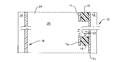
An electrophoretic display device 10 which may employ the segmented
anode configuration of the present invention may be seen, for example, by
reference to FIG. 1. It will, however, be understood by those of ordinary
skill in
the art that the description of EPID 10 is for illustrative purposes only and
that any
EPID configuration may employ the novel segmented anode and associated erase
control circuitry to be herein described.
As seen in FIG. 1, the illustrative electrophoretic display device 10 includes
two
separated substrates 12 and 14, at least one of which is transparent by way of
being a material such as glass or plastic. Substrate 12, which is preferably
coated
with an extremely thin layer of indium tin oxide (ITO), acts as a port through
which a viewer of the display may discern image information set forth thereon.
The ITO layers is extremely thin, on the order of 100 to 300 angstroms, and
hence
is truly transparent. Utilizing a technique such as that described in U. S.
Patent No.
4,732,830, a pattern of horizontal lines is etched on the surface of the ITO
layer to
form a plurality of row or cathode conductors X, through X".
Disposed upon the group of cathode conductors are a series of insulator
members 16. The insulator members are formed from a photoresist layer such as
a
phenolic resin impregnated with photoactive material which layer is deposited
over the cathode line structure. The photoresist layer is treated to
selectively
remove photoresist where a plurality of vertical lines are deposited upon the
insulator members 16 to form a plurality of column conductors or grid
electrodes
Y, through Yn perpendicular to the cathode conductors. Each grid electrode, as
indicated, is positioned above associated cathode lines and insulated
therefrom at
the areas of intersection (pixels) by the insulator members 16.
'~ i
2172552
WO 95/10107 PCT/US94/10871
8
A segmented anode structure, which may for example be
fabricated by e~_ching a layer of ITO deposited on substrate 14 in accordance
with a conventional etching technique, is disposed on substrate 14 and is
identified generally by the reference numeral 18. An insulating structure (not
shown) maintains the separated substrates and associated cathodes, grid
electrodes, and anode segments, and electrophoretic suspension layer 20. The
electrophoretic suspension layer 20 includes a dispersion of an
electrophoretic
material in the form of charged particles 22 in a finely divided powder form
suspended in a dielectric fluid 24.
As one can readily ascertain upon reference to the previously
cited patents, the pigment at the intersections of selected rows and columns
is
forced out of wells associated therewith (not shown) by selectively applying
voltages to the rows and columns. If the cathode-grid structure is negatively
biased relative to the anode and the suspension comprises light-colored,
negatively charged pigment particles suspended in a dark colored medium, then
application of operating potentials to the X-Y intersections will cause
particles
at that location to migrate to the anode, thereby creating an image by the
light
color of the particles against the dark color of the suspension medium, or by
the absence of particles at the cathode. Consequently, if a negative potential
bias is applied to the anode, the particles will migrate back towards the grid-
cathode structure, thereby erasing all or part of the image.
The movement of pigment particles toward the grid-cathode
structure during an erase operation is not instantaneous but requires a period
of time, which depends upon the dimensions of the display, the applied
voltages, and the properties of the suspension. Applying a negative potential
for too short a period of time to an anode line segment thus results only in
an
incomplete or partial erasure of a corresponding character line. Accordingly,
a
character may be selectively erased or written over without substantially
....IJVO 95/10107
217 2 5 5 2 PCT/US94/10871
9
affecting the remainder of the character line by partially erasing the
character
line, rewriting those characters which are to remain displayed, and repeating
the procedure until the selected character is completely erased or replaced by
another character. This essentially is the basis of the present application
and
such techniques for accomplishing this will be further described.
The present invention is particularly directed to an improved
anode structure which allows erasing of one or more selected characters of a
given line without erasing all characters of that line, thereby allowing a new
frame having substantial portions the same as the previous frame to be written
in less time. Referring to FIG. 2, anode structure 18 comprises a multiplicity
of individual anode conductor segments Zl through Z", with each respective
conductor segment being exactly opposite a group of grid and cathode
intersections corresponding to a character line of the display. As will soon
be
apparent, the thickness of the row or cathode conductors and the spacing
therebetween, as well as the height of the character to be displayed,
determine
the nominal width of the character blocks. Typically, each of the row
conductors will have a width on the order of 112 ~,m while separation between
adjacent conductors is typically 15 Vim. Accordingly, if the display is to
utilize
characters which are 26 pixels high, then each anode line segment should be
3.302 mm wide.
As shown in FIG. 2, each anode line segment is isolated from
adjacent blocks by a narrow insulating region 26 that is aligned with inactive
areas 28 between cathode lines. It will, therefore, be apparent that the
dimensions of these inactive areas will also be a function of the spacing
between adjacent cathode conductors. Each character line may comprise a
single anode segment or a plurality of independently addressable segments. In
accordance with an illustrative embodiment of a display for primarily twenty-
four lines of text characters at a time, depicted in FIG. 3 are 4 segments Zl
2 i 72552
WO 95/10107 PCT/1JS94/10871
through Z24, in the form of elongated rectangular strips in parallel with and
electrically insulated from each other. Each anode line segment has a suitable
driving amplifier circuit shown in modular form and indicated by reference
numerals 30, 32, 34, and 36, which amplifiers are in turn coupled to an anode
5 address module 37. The driver amplifiers and address module are fabricated
by typical integrated circuit techniques and may, for example, be CMOS
devices, all of which are well known and many of which are available as
conventional integrated circuit chips. As each anode segment is insulated from
each other, one or more anode segments corresponding to display lines having
10 characters to be selectively erased can be briefly switched to a partial
erase
potential while other anode segments are maintained at the write or hold
potential. The result is that one or more character lines can be partially
erased
while the other character lines are maintained at the write or hold potential.
An X-Y Write Control module (not shown), in a writing phase,
applies a voltage to selected cathode and grid lines. Referring to FIG. 4,
there
is shown a top view of a typical X-Y matrix consisting of cathode lines which
are arranged in the horizontal plane and grid lines which are perpendicular to
the cathode lines and insulated therefrom. Thus, there are shown in FIG. 4
four cathode lines, which cathode lines are designated X,, X2, X3, and X26 and
which are indicative of a character line 38 which is 26 pixels high. It is, of
course, understood that the number of cathode lines in the X direction may
consist of hundreds of thousands, depending upon the size of the display. As
indicated, insulated from the cathode lines and perpendicular thereto, there
are
also shown four grid lines, Y1, Y16, Ym, and Y3, indicative of two characters
Cl
and CZ of character line 38, each character being 16 pixels wide. It should
also
be understood that there are many more grid lines associated with a typical
display, the precise number depending upon the number of characters to be
displayed on each line.
WO 95/10107
2 i 7 2 5 5 2 pCT~S94/10871
11
As seen in FIG. 4, each cathode line has a suitable driving
amplifier circuit shown in modular form and indicated by reference numerals
40, 42, 44, and 46. In like manner, each grid line has a suitable driving
amplifier referenced by modules 48, S0, 52, and 54. The driver amplifiers are
S fabricated by typical integrated circuit techniques and may, for example, be
CMOS devices, all of which are well known and many of which are available as
conventional integrated circuit chips.
As in the case of prior art EPID displays, the display of the
present invention can typically be operated in an erase mode, a hold mode, or
a writing mode. In a full erase mode, where all character lines of the display
are to be erased, all anode line segments are placed at a negative potential
while the cathodes as lines X, to X26 are operated at a low potential, or at
zero. In this mode, the grid lines as Yl to Y3, are operated at a positive
potential. In the hold mode, all anode segments not containing a character to
be erased or written over are made positive while the grids are placed at
negative potential and the cathodes are held at a positive potential. As one
can understand from the above, the grid lines operate between negative and
positive voltages. The cathode lines operate between zero and positive
voltages. In the write mode, the anode segments are held positive while grid
lines which are being written are placed at positive potential while non-
writing
grid lines are placed at negative potential. In this mode, the writing
cathodes
are operated at zero potential. Thus, based on the X-Y matrix, one can
produce any alpha numeric character.
As indicated, however, the display of the present invention is also
operable in a selective character erase mode in which a single character of a
given character line as 38 can be erased. Such selective erasure is obtained
in
accordance with an illustrative embodiment of the present invention by briefly
biassing the anode line segment negative relative to the grid-cathode matrix
for
2172552
W0 95/10107 PCT/US94/10871
12
a time interval sufficient to partially obscure the cathode-grid intersections
comprising the corresponding character line but not long enough to render the
character line illegible. During this time, some of the pigment particles move
relative to the grid-cathode intersections such that after each application of
the
negative bias, characters to be erased appear progressively lighter. Those
characters of character line 38 which are not to be erased are rewritten by
using the "write mode" procedure described above. In accordance with the
present invention, sequential applications of negative bias to the selected
anode
segments alternated with "write mode" procedure for pixels which are not to be
erased are required before the selected characters are completely erased or
written over.
Consider characters Cl and Cz of character line 38, in which
character C, to be erased is defined by the intersections of cathode lines Xl
through X26 and grid lines Yl through Y16 and character Cz to remain displayed
is defined by the intersections of grid lines Y1~ through Y3z with the
aforementioned cathode lines. With reference to FIG. S, there is illustrated
an
example of timing relationships and waveforms for pulsing the grid-cathode
intersections and the anode segment or segments corresponding to character
line 38 according to the teachings of the present invention. In FIG. 5, there
are illustrated four waveforms (A.,B,C,D) indicative of the wave forms
provided
by the driving amplifiers during the selective character erase mode. With
initial reference to FIG. SA, it can be seen that during time intervals t~
through
tz, cathode lines X1 through Xz6 remain at a positive potential + V,;. With
reference to FIGS. SB, SC and SD, it will be observed that as erasure of
character C~ is initiated during time interval tz, grid lines Y1 through Y3z
remain at a negative voltage -V~ while a negative potential - Ve is applied to
anode segment Zl. Time interval tz, which may be on the order of several
~~WO 95/10107 - , 21 l 2 5 5 2 PCT/US94/10871
13
milliseconds, is selected so that partial erasure of character line 38 is
accomplished without rendering the same illegible.
During subsequent interval t3, it will be observed that cathode
lines X1 through X26 are sequentially lowered to 0 volts and grid lines Yl
through Y16 remain at a negative potential -V~ while a positive potential + Va
is applied to anode segment Zl.
Grid lines Y~~ - Y32 are made positive or left negative as each cathode line
Xl -
X26 is sequentially lowered to 0 volts to maintain the original character.
This
alternating sequence is repeated until character Cl is completely erased and
character CZ is left unchanged. Thus, character CZ is partially rewritten
after
each application of a negative bias to the anode, such that at the end only
the
selected character Cl is erased.
It will, of course, be understood that instead of erasing character
as C,, it is possible to partially replace that character with a new
character.
This may be accomplished by partially rewriting the replacement character
after each application of negative bias to the corresponding anode segment,
utilizing a sequence such as that illustrated in FIG. SD. Moreover, it should
also be emphasized that a given character line may be served by any desired
number of anode segments and that pulses as described herein may be applied
to each independently of the others.
Although the present invention has been described in detail, it
should be understood that various changes, substitutions, and alterations can
be
made herein without departing from the spirit and scope of the invention as
defined in the appended claims.