Note : Les descriptions sont présentées dans la langue officielle dans laquelle elles ont été soumises.
2 1 72704
SPECIFICATION
TITLE
"CIRCUIT ARRANGEMENT FOR COMPENSATING FREQUENCY DEVIATIONS OF A
VOLTAGE-CONTROLLED OSCILLATOR, USING A SECOND OSCILLATOR"
BACKGROUND OF THE INVENTION
Field of the Invention
Phase detectors are used in phase locked loops for clock recovery from a data
signal. A phase detector supplies an output signal corresponding to the phase difference
between its two input signals. The phase detector does not assist in clock recovery if the
simultaneous frequency difference between the two phase detector input signals is too
large. The frequency range of the voltage-controlled oscillator (VCO) must be as small
as possible in order for the phase lock loop to lock onto the clock frequency.
Description of the Prior Art
The frequency range of a VCO integrated in ECL technology depends strongly on
the operating temperature of the chip and the manufacturing-conditioned scatter of the
semiconductor parameters. In order to ensure the oscillator oscillates at the desired
frequency, the tunable frequency range is designed to be wide enough that the desired
frequency can be reliably achieved not only in the normal case but also in the worst case;
for this purpose the tuning range must be correspondingly large (larger than an octave).
However, it is then no longer certain that the phase locked loop locks directly onto the
correct frequency; the loop could for example also lock onto the double of this frequency.
This can be counteracted by adding the actuating signal of a reference phase
locked loop to the actuating signal of the VCO. This requires a corresponding circuit
2 1 72704
outlay for such a reference clock and can lead to unwanted beat effects.
For frequency stabilization of a VCO in a thermostatic housing, it is known to
provide an additional oscillator in the thermostatic housing as a temperature sensor. An
actuating signal for the other oscillator and the control signal for thermostatic control are
provided depending on the difference between the two oscillator frequencies.
United States Patent No. 3,713,033 discloses a system for digitally correcting the
frequency of a crystal oscillator as a function of ambient temperature. A circuit
arrangement in which the frequency of another oscillator controlled by a thermistor is
counted by a frequency counter. The count result is used to control a preprogrammed
ROM. The ROM emits a frequency correction signal that after A/D conversion corrects
the frequency of the quartz oscillator. The oscillator is temperature-compensated by
another means.
United States Patent No. 4,492,933 discloses a temperature compensation circuit
for an oscillator circuit having a frequency response that is parabolic with respect to
temperature. A circuit arrangement in an AC integrator circuit transforms a linear
sawtooth signal into a parabolic sawtooth signal. The parabola flanks are sampled at a
temperature-dependent phase. The flanks are then sampled at a corresponding different
amplitude, by a monostable multivibrator, which is triggered by a comparator charged
with the linear sawtooth signal and a temperature signal. The sampled signal amplitude
controls the varactor.
These oscillator circuits are consistently expensive.
21 727Q4
SUMMARY OF THE INVENTION
The invention provides a high-precision monolithic integrated VCO with a low
circuit outlay.
The invention concer"s a circuit arrangement for compensating frequency
deviations of a VCO using a second oscillator. This circuit arrangement is achieved on
the same chip with a monolithic integrated VCO, and an additional, similar oscillator that
is not externally voltage-controlled. An additional control signal, opposed to the influence
of temperature or parameter on the oscillator frequency, is derived from the oscillation
frequency to the additional oscillator. In addition, in an alternative embodiment of the
invention the output of the additional oscillator can be connected with an additional
control input of the VCO via an iterative network of a monostable multivibrator and a
subsequent low-pass.
The invention uses information derived from a reference clock. This information
concerns the frequency of a similar oscillator, which is dependent on the temperature and
the parameters of the chip in the same way as the VCO. The nominal frequencies of the
two oscillators may be completely different. The invention compensates by providing a
parameter-conditioned, temperature-conditioned frequency deviation of a monolithic
integrated VCO.
Further characteristic features of the invention are explained below on the basis of
an exemplary embodiment shown in the accompanying drawings.
DETAILED DESCRIPTION OF THE DRAWINGS
21 72~Q4
Figure 1 is a block diagram of a preferred embodiment of a monolithic integrated
VCO circuit.
Figure 2 is a block diagram showing circuit details of the monolithic integrated
VCO circuit accordiilg to the invention.
Figure 3 is a schematic diagram of the monostable multivibrator.
Figure 4 is a schematic diagram of the ECL buffer circuits.
Figure 5 is a schematic diagram of the ECL level shifters.
Figure 6 is a schematic diagram of the control element for frequency control.
DETAILED DESCRIPTION OF THE PREFERRED EMBODIMENTS
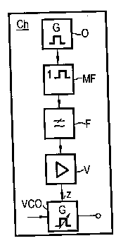
Figure 1 is a preferred embodiment of the voltage-controlled oscillator circuit VCO
monolithically integrated on a chip Ch. An oscillator O is provided on the chip Ch in
addition to the voltage-controlled oscillator VCO. The oscillator O is not externally
voltage-controlled. The oscillation frequency of the oscillator O in principle depends on
the operating temperature and the manufacturing parameters of the chip Ch the same
way as the frequency of the voltage-controlled oscillator VCO depends on these
characteristics. An additional control signal for the voltage-controlled oscillator VCO is
derived from the oscillation frequency of the additional oscillator O. This additional
control signal is opposed to the influence of the temperature and parameter
characteristics of the chip Ch on the oscillator frequency of the voltage-controlled
oscillator VCO.
As shown in Figure 1, the output Y of the additional oscillator O is connected to an
2 ~ 7~04
additional control input z of the voltage-controlled oscillator VCO via the iterative network
of a monostable multivibrator MF, a low-pass filter F and an amplifier V. The output
impulses of the oscillator O are lengthened to a fixed value (about 1/4 of the period
duration, given normal parameters and average temperature) by the monostable
multivibrator MF. The pulse/pause relation of the square-pulse sequence depends on
the oscillation frequency of the oscillator 0. The direct component of this square-pulse
sequence is brought out by the subsequent low-pass filter F. After amplification by the
subsequent amplifier V, the amplified direct component then serves as an actuating
signal for the voltage-controlled square-pulse oscillator VCO, counteracting possible
frequency deviations.
In Figure 2, a block diagram shows circuit details of a monolithic integrated
voltage-controlled oscillator circuit VCO according to the invention. The oscillator O is
formed with an inverting feedback-coupled iterative network of buffer circuits B and level
shifters P. The actual voltage-controlled square pulse oscillator VCO is in principle
formed in the same way, with a positive feedback-coupled iterative network of buffer
circuits B and level shifters S. A control element M for frequency control is also provided
in the iterative network. An iterative network of a monostable multivibrator MF, a low-
pass F and an amplifier V is again provided between the oscillator O and the additional
control input z of the voltage-controlled oscillator VCO.
The monostable multivibrator MF is implemented as shown in Figure 3. The time-
determining elements of the ECL monostable multivibrator MF are the resistance R and
2172704
the capacilance C. These must be implemented so that they are as independent as
possible of the manufacturing parameters. This can be achieved when given a large
resistance and the exploitation of the capacitance C between two wiring levels in the chip
Ch. Transistor Q1 limits the voltage over the RC element, so that the capacitor C is
always charged at a defined voltage. If warranted, the temperature dependency can be
compensated by correction of the control voltage of the other transistor Q of the output
buffer in the monostable multivibrator shown in Figure 3. This is achieved by means of a
corresponding temperature-dependent control of the associated current source, in a way
which need not be further explained here.
Figure 4 shows the implementation of the ECL buffer circuits B.
Figure 5 shows the ECL level shifters S. The ECL buffer circuits B are
distinguished from the ECL level shifters S in that the cross current power sources are
not controllable. The run time of an ECL buffer B depends on the cross current of the
preceding level shifter P or S. The larger the cross current, the smaller the run time
(within certain limits). This can be exploited to change the frequency of the oscillator.
The control element M for frequency control, provided in the voltage-controlled
square-pulse oscillator VCO (in Figure 1 and Figure 2) can be implemented as shown in
Figure 6. The frequency control M is an ECL analog signal multiplexer. Two inputs A/AX
and B/BX in the voltage-controlled square pulse oscillator VCO as shown in Figure 2 are
connected to two consecutive level shifters S (via a buffer circuit B). The level shifters S
control input C/CX forms the frequency control input of the voltage-controlled oscillator
- 21 727~4
VCO (in Figure 1 and Figure 2). The voltage supplied between the control input
connections C and CX, allows for setting the strength of the signal appearing at the input
A/AX or at the input B/BX. The strength of this signal affects the output Q/QX.
Although modifications and changes may be suggested by those skilled in the art,
it is the intention of the inventors to embody within the patent warranted hereon all
changes and modifications as reasonably and properly come within the scope of their
conl, ibution to the art.