Note : Les descriptions sont présentées dans la langue officielle dans laquelle elles ont été soumises.
CA 02173237 1999-02-O1
Optical switching device
BACKGROUND TO THE INVENTION
The present invention relates to a non-linear optical
S switch, and in particular to a switch incorporating a
semiconductor optical gain medium which imposes a
switchable phase change on an optical signal, and to
optical circuits incorporating such a switch.
Non-linear optical switches of the type the present
invention is concerned with, are potentially of use in a
wide variety of fields. For example, in optical
telecommunications systems, such switches may form the core
of a demultiplexer for use with an OTDM (optical time
division multiplexing). pulse stream. A demultiplexer using
a semiconductor non-linear element in a non-linear loop
mirror configuration can operate at bit rates as high as
lOGHz. Also in the field of optical telecommunications
systems, the use of semiconductor non-linear elements has
been proposed for clock-recovery. Our co-pending
Canadian application No. 2,118,407 discloses and claims
'such clock-recovery circuits incorporating non-linear
elements in the cavity of a mode-locked laser system.
Hitherto, using conventional semiconductor non-linear
elements, the performance of such optical switches has been
limited significantly by the recovery time of the
semiconductor optical gain medium. High electrical bias
fields have been used with the semiconductor laser medium
to maximise the recovery speed, but even so for some
applications, such as clock recovery, it has still not
proved possible to obtain the recovery times necessary for
operation at the highest data rates.
SUMMARY OF THE INVENTION
According to a first aspect of the present invention
there is provided a non-linear optical phase switch
including a semiconductor optical gain medium arranged to
WO 95/10795 , PCT/GB94/02240
switch a signal at a first wavelength (~3) in response to
a control signal at a second wavelength (~2) applied to the
optical gain medium, the refractive index of the gain
medium being modified in response to the control signal,
characterised by means for applying an optical holding
signal at a third wavelength (~~) to the gain!medium, the
optical holding signal pumping the semiconductor optical
gain medium thereby fixing the Fermi level of the gain
medium.
The present invention uses a third light beam applied
to the semiconductor gain medium to provide a; non-linear
switching element with a reduced recovery time, and a
recovery time which moreover can be controlled directly
simply by varying the intensity of the holding,beam. The
holding beam, by clamping the Fermi level of the conduction
band in the gain medium, ensures that the response of the
non-linear switching element to the control' signal is
uniform, even where the control signal itself is irregular.
This is of particular significance in clock-recovery
applications, where the control signal is a data stream
which may, for example, include a long sequence of zeros.
The system may be operated with wavelength-degeneracy,
that is to say the wavelength of the holding beam may be
equal to one or both of the other wavelengths. ;However it
is much preferred that the three wavelengths should all be
different. This makes possible optimisation of the
performance of the device by selecting suitable wavelengths
in accordance with the wavelength-gain characteristic of
the amplifier. It also makes possible separation of the
different beams using, for example, WDM couplers.
There are few restrictions on the wavelengths which
may be selected for the signal ~3. The closer it is to the ,
band-gap equivalent wavelength, the better the phase
modulation, the nearer it is to the holding beam~the better
the amplitude modulation. It may also be placed above the
holding beam energy (i.e. in loss) - this was the case in
recent successful clock recovery experiments at 10 and
WO 95/10795 ~ rj PCT/GB94/02240
3
2oGHz. A further alternative possible position for the
signal wavelength is below the band-gap energy of the
semiconductor material. The signal is then in
transparency.
The optical holding signal may be a continuous wave
(cw) signal, or alternatively may be a pulsed signal timed
to follow (that is come after in the time domain) the
control signal.
Preferably the switch comprises a non-linear loop
mirror (NOLM) incorporating a semiconductor laser amplifier
(SLA) as its non-linear element. As further discussed
below, such a switch is particularly suitable for use as an
OTDM demultiplexer, and may then use a TOAD [2]
configuration.
Although the present invention has been found to be
particularly effective in NOLMs, it may also be used with
other switching structures. For example, the semiconductor
optical gain medium may be arranged in one arm of a Mach
Zender interferometer. This may be formed as an integrated
solid state device. Such a configuration provides enhanced
time resolution, since the response of the switch is no
longer limited by the transit time through an optical loop
as in the NOLM configuration.
Optical switches embodying the present invention may
be used in OTDM demultiplexers, as described, for example,
in 'The use of GalnAsP amplifiers for 40Gbit/s signal
processing' A.D. Ellis, D.M. Spirit Postdeadline Paper,
Nonlinear Guided-Wave Phenomena, Cambridge, England Sept
20-22, 1993.
Preferably a relatively high electrical bias is
applied to the semiconductor gain medium such that the
holding beam experiences gain sufficient at least
substantially to eliminate attenuation of the holding beam
on its passage through the amplifier. More preferably the
holding beam has a relatively low launch power such that it
does not saturate the gain medium immediately on entry to
CA 02173237 1999-02-O1
4
the medium, and the semiconductor is electrically biased to
provide net gain to the holding beam.
The present inventor has found that the electrical
bias applied to the amplifier has a significant effect on
S the recovery rate, and that this rate can be optimised by
increasing the electrical bias to a level where the gain
experienced by the holding beam is at least sufficent to
counteract the attenuation which would otherwise be
experienced by the holding beam. In this manner, the
optical input power required for the holding beam can be
made relatively small, most of the power for the holding
beam being provided by gain within the amplifier in
response to the applied electrical power.
Optical switches embodying the present invention may
be used in clock recovery and/or signal regeneration
circuits as described and claimed in our pending
Canadian application No. 2,118,407 filed 26 April 1993. They
may also be used in optical pulse generator circuits, as
described and claimed in our co-pending Canadian application
No. 2,171,337 entitled "Optical Switch", claiming priority from
EP 93308067.3. The present invention is however by no means
limited to use in these fields, and may be used wherever an
optical switching element of enhanced and readily controllable
recovery time is required.
According to a second aspect of the present invention
there is provided an OTDM demultiplexer including a switch.
According to a third aspect of the present invention
there is provided an optical pulse generator comprising a
switch according to the first aspect connected in the
optical cavity of a mode-locked laser, in use the control
signal applied to the gain medium cross-phase modulating
pulses propagating in the cavity.
According to a fourth aspect of the present invention
there is provided a method of switching an optical signal
comprising directing an optical . signal at a first
wavelength through a semiconductor gain medium and
WO 95/10795 ~ 3 ~ PCT/GB94/02240
modifying the refractive index of the gain medium in
response to a control signal at a second wavelength,
characterised by applying an optical signal at a third
wavelength to the gain medium, thereby pumping the medium.
5
BRIEF DESCRIPTION OF THE DRAWINGS
Embodiments of the present invention will now be
described, by way of example only, with reference to the
accompanying drawings in which:
Figure 1 is a diagram illustrating a demultiplexer
incorporating the switch of the present inventions;
Figure 2 shows a clock recovery circuit incorporating
the switch of the present invention;
Figure 3 is a diagram illustrating the energy levels
of a prior art semiconductor laser;
Figures 4a and 4b show the variation with time of the
carrier population and phase of the semiconductor of Figure
3 for a regular clock stream;
Figure 5 is an energy level diagram for a switch
embodying the present invention;
Figure 6 shows the population change as a function of
time for the clock recovery circuit of Figure 2;
Figure 7 is a timing diagram for a pulsed holding
beam;
Figure 8 is a graph showing the recovery time of the
switch;
Figures 9a and 9b are views of an active waveguide
device;
Figures l0a and lOb are plots of amplitude and phase
modulation respectively for different applied bias
currents;
r , Figure 11 shows optical power distribution along an
SLA; and
Figure 12 shows optimum wavelengths for a phase
modulation switch.
DESCRIPTION OF EXAMPLES
CA 02173237 1999-02-O1
6
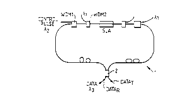
Figure 1 shows a first system embodying the present
invention. A non-linear loop mirror (NOLM) configured to
operate as a demultiplexer includes a semiconductor laser
amplifier (SLA) as the non-linear element in the loop. The
loop functions in a conventional fashion, with data input
via a coupler 2 being either transmitted (T) or reflected
(R) depending upon the phase change it experiences within
the loop. That phase change is determined by the state of
the semiconductor laser amplifier. The state of the
amplifier is switched in response to an input control
signal at a wavelength ~z. This control signal is coupled
into the loop via a wavelength division multiplexes WDM1.
In the system embodying the present invention, a
further signal, the holding signal at wavelength ~1 is
coupled into the semiconductor laser amplifier via a second
wavelength division multiplexes WDM2. As further described
below, this has the effect of optically biasing the
semiconductor laser amplifier so as to reduce its recovery
time after the application of each control pulse from the
pulse source. This enables the demultiplexer to function
at an increased bit rate.
Figure 2 shows a second embodiment of the present
invention. In this case, the circuit is a clock-recovery
circuit of the type described in our above-cited co-pending
Canadian application No. 2,118,407. The
semiconductor laser amplifier in this case acts as a
modulator connected in the optical cavity of a ring-laser.
The "control signal"~in this case is a data stream applied
to the semiconductor laser. Cross-phase modulation and
amplitude modulation of the applied data stream and the
pulses in the laser cavity results in the generation within
the cavity of a pulse train locked to the timing waveform
of the data stream. This pulse train is coupled out of the
cavity to provide a clock for subsequent optical processing
stages. As in the first circuit described above, when the
present invention is applied in this context, an additional
optical signal provided by the holding beam at wavelength
CA 02173237 1999-02-O1
f. _ 7
~~ is applied to the semiconductor laser amplifier. As
above, this biases the amplifier to speed the recovery time
and also, crucially in this particular application, fixes
the Fermi level of the semiconductor gain medium in such a
way as to ensure that:
(1) there is a constant phase response to the applied
modulating sigr_31;
(2) The phase does not change in the absence of a
signal (i.e. an absence corresponding to a 0).
These effects are of value where data streams are to
be used as the "clock" stream (~z), for optical processing
with this device, whatever the specific application (e. g.
wavelength conversion, demultiplexing, etc.).
In a circuit as described above for use in clock
recovery, if the data stream is a repetitive signal having
a repeat period equal to or an integer multiple of the
cavity round trip time, then rather than outputting a
uniform clock it produces a pulse stream having bits in
bit-positions corresponding to those channels in the
repetitive signal which carry data, and no bits in
positions corresponding to those channels in the signal
which are OFF, i.e. permanently set to zero. As described
and claimed in our co-pending Canadian application No.
2,171,337, the circuit then functions as a programmable
ulse
p generator which replicates the input signal pattern
and may be used, for example, in controlling an all-optical
demultiplexer in which the output of the pulse generator
gates an optical switch such as an NOLM.
Figure 3 illustrates the energy levels of a
conventional semiconductor laser amplifier. Such
. amplifiers as used hitherto for switching applications have
received signals at just two wavelengths, the signal
wavelength (for example the wavelength of the data in a de-
multiplexer) and a clock or control signal at a second
wavelength. In the example of the circuit disclosed in [1]
the clock is at a pulse rate of lOGHz. A high electrical
WO 95/10795 PCT/GB94/02240
8
bias field is applied to the semiconductor to provide a
recovery time on a time scale of approximately 100psec.
The clock pulse maintains the Fermi level at an average
energy about which it fluctuates. The Fermi level is ,
forced down as the clock saturates the gain, and then
recovers (after the clock pulse has left) via~electron and _
hole injection into the conduction and valence bands under
the influence of the bias field. The carrier (electron and
hole) population is then swept out again by the next clock
pulse. The carrier population redistribution caused by the
clock pulse is responsible for the ~ phase shift
experienced by the signal pulse. The fact that the Fermi
level returns to the same position is due to; the regular
nature of the clock signal. The carrier population and
phase change at the signal wavelength are shown in Figures
4a and 4b. The sign of the nonlinearity (or phase change)
may be either positive or negative, depending upon the
specific wavelengths selected for the three beams.
In clock recovery applications, a non-regular
datastream replaces the clock and the Fermi level is no
longer pinned as before since there is not necessarily a
regular pulse at the bit-rate. For example, a data
sequence of 1101001 would give the carrier population
change shown in Figure 4c . As seen in this .Figure, the
change in response to the 1' s may not be constant and there
is a time-varying phase change for the 0's.
As already described, in the systems embodying the
present invention the signal and control ,wavelengths
supplied to the semiconductor are supplemented by a holding
beam at a third wavelength. Figure 5 shows the energy
level diagram for the semiconductor in these circumstances.
. Now the Fermi level is clamped most of the time by the ,
holding beam at wavelength ~~. When a clock or control
pulse arrives, the excess population of carriers is swept
out causing a change in the refractive index ~;at ~3. The
carrier population in the ground state is now. pumped back
by the continuous wave holding beam, very quickly if the
WO 95/10795 PCT/GB94102240
9 _
beam is sufficiently intense. Thus the laser amplifier
rapidly recovers its initial state. In the absence of a
clock pulse, the gain is still clamped to the same value
by
the presence of the holding beam. The population change
for a clock recovery circuit receiving the data sequence
1101001 now takes the form shown in Figure 6. By contrast
with the prior art, the phase does not now vary when 0's
are present and the phase change on arrival of the next
"clock" (driving) pulse is constant. Also, most
importantly, the gain recovery rate is increased due to
the
presence of the optical bias which pumps carriers which
have been stimulated down into the valence band back into
the conduction band. The rate of recovery is directly
proportional to the intensity of the optical bias supplied
by the holding beam. It is important that this rate of
recovery should be slower than the rate of population
increase in the valence band due to the clock pulse,
otherwise no significant population change or phase change
would occur. However, in a typical data stream, there is
1:10 mark to space ratio, so that it is only necessary to
ensure that recovery takes place on the time scale of the
bit period, not on the time scale of the clock pulse. For
example, for a lOGbit clock rate, the optical pulse is
lOpsec and the bit period is 100psec: the recovery has to
be on the time scale then of 100psec. This is convenient,
since the rate of removal of carriers when the clock pulse
is on will not be large (1/10 of the rate of injection of
carriers into the valence band).
As an alternative to using a continuous wave holding
beam, the beam maybe pulsed so that the gain is only
replenished after the clock or control pulse has gone, as
shown in Figure 7.
The optical bias provided by the holding beam maybe
used in place of electrical bias or in addition to
electrical bias. The electrical bias is useful; it aids
the recovery rate and supplies energy to the device, and
for the embodiments discussed below provide one of the
WO 95/10795 ,PCT/GB94/02240
operating parameters. For the preferred embodiments, high
bias currents (-.200 mA) are desirable.
The approach adopted in the present invention gives
the potential for extremely compact devices. The SLA may
5 be pumped from one side at either the clock or holding beam
wavelength using another laser or a surface emitting laser. ,
The SLA maybe any semiconductor laser structure such as a
bulk or quantum well, or a quantum wire (even quantum dot)
device.
10 Although in the first example described;above, the
holding wavelength is shorter than that of either the
wavelength of the control signal or the wavelength of the
data carrying signal, the wavelengths maybe assigned
differently. For example, in clock recovery,', it may be
advantageous to use the longer wavelength ~Z for the bias
or holding beam, and the shortest wavelength.~~ for the
data stream. Then the data stream adds to the gain of the
system. This selection of wavelengths has the advantage
that any amplitude modulation caused by the data pulses
tends to be such as to add to the gain of the recovered
clock pulses thereby providing a "shutter" effect. The
excess gain is now swept out by stimulated emission at the
holding beam wavelength. This arrangement reverses the
sign of the refractive index change, which may be useful in
the performance of the ring laser part of !the clock
recovery circuit.
The minimum wavelength separation between hold
and clock (AZ) is governed by the phase change:needed for
the specific application (~r for OTDM, ~r/10 or less for
clock recovery), which sets the minimum carrier population
change needed (10"17 cm3 for ~r). There must be at least
. this excess carrier population existing between the two
wavelengths. The separation is therefore dependant upon a
detailed knowledge of the band structure (its parabolicity
or otherwise), and the density of states'. The switching
energy (for a n phase change) is 3 picoJoules, Energies for
a clock recovery circuit requiring a ~r/10 phase~change are
WO 95/10795 ~, ~ PCT/GB94/a2240
11
about 0.3pJ. A recovery time of lops requires about 300mW
of optical power for the OTDM embodiment.
The inventor conducted a series of measurements of the
recovery rates of a semiconductor laser amplifier (SLA)
with and without the intense optical cw "holding beam
(referred to as ~~ above) present in the amplifier and also
investigated the effect of electrical bias on the recovery
rate, with the holding beam on. These measurements gave
amplitude and phase changes imparted on a weak "probe"
pulse which passed through the amplifier after a stronger
"excite" pulse had changed the properties of the SLA. The
experiment hence gave time-resolved measurements of the
recovery rates of the amplifier.
The power in the holding beam was -.37 mW in the fibre
immediately before the amplifier. Assuming a 3 dB coupling
loss, the power launched into the SLA was --18 mW. The
wavelength of the holding beam was 1535 nm. The "excite"
and "probe" pulses correspond to the "clock " pulses
and the "data" (or "signal") pulses (~3). In these
experiments, the "excite" and "probe" pulses have the same
wavelength, 1562nm. The pulse duration was ~lOps for both
pulses, and the "excite" pulse energy was ~l.SpJ (again
measured in the fibre prior to launch into the SLA (hence
a launched energy of .7pJ). The electrical bias was
varied from ~2omA to 200mA, to observe the effect on
recovery rate. The results of these experiments are in
Figures l0a and lOb which give the amplitude and phase
modulation (measured simultaneously). As may be seen, the
effect of increasing the electrical bias is dramatic. The
results are summarised in Table 1 below. Note that the
(1/e) lifetimes were taken from straight line fits to log
plots of the data.
WO 95/10795 ~ PCT/GB94/02240
12
TABLE 1
CW Beam Power Electrical bias current Lifetime
(mW) (mA) (ps)
0 23.3 ' 500
37 23.3 105
37 100 . 0 -.45
37 199.9 !13.2
Note that the 100mA data is not shown in the figures.
It is believed that the dramatic effect of increasing
the bias current is mostly due to longitudinal effects in
the amplifier. At low bias currents the cw beam saturates
the available gain but experiences loss as it passes
through the amplifier due to scattering losses. This loss
was measured to be -.lOdB for a bias current of -.25mA. At
a bias of 200mA the cw beam experiences almost no loss .
Hence at low bias there is a 20mW power only in~ the part of
the front of the SLA. At high bias, there is uniform
illumination throughout the length of the SLA. ~ A schematic
of this is given in Figure 11. We conclude,' therefore,
that best (fastest) operation will be with high bias
currents (200mA or greater). This is important, since it
reduces the need for excessively large holding beam powers,
which are difficult to obtain practically. A~t high bias
currents, there may be carrier number density effects which
will decrease the lifetime in the absence of the holding
beam, and may reduce the lifetime with the holding beam.
Leakage effects may also decrease the lifetime.
In a further experiment by the inventor, still shorter
lifetimes were obtained using a lower power holding beam,
at powers in the launch fibre of 5-30mW, ~iith a bias
current of 30omA. The response lifetime was then less than
or equal to the time resolution of the experimental system,
i.e. s lops. At these lower launch powers the holding beam
WO 95/10795 PCT/GB94/02240
13 ~.:~
~~z~~
.
does not saturate the gain of the semiconductor on entry
and experiences greater amplification.
The SLA has a natural lifetime of about lns and a
length of approximately 0.5mm. This length is much shorter
than the length of the fibre modulators previously proposed
for use in clock recovery circuits and so makes possible
a
very large reduction in latency, that is the time taken for
the circuit to respond to an input signal and output a
clock signal. The SLA is also able to offer broadband
operation over the gain spectrum of the amplifier,
typically a bandwidth of approximately 100nm. The position
in the energy diagram of the signal (~3) suffers few
restrictions. The closer it is to the band gap equivalent
wavelength, the better the pure FM operation (i.e. phase
modulation), the nearer the holding beam, the better the
AM
modulation (i.e. amplitude modulation). It may also be
placed above the holding beam energy (i.e. in loss) - this
was the case in the recent successful clock recovery
experiments at 10 and 20 GHz.
Figure 12 plots gain as a function of wavelength ( i . a
.
inverse energy). We assume a saturating beam at ~~, within
the gain bandwidth of the SLA. The "clock" or "control"
pulse at ~2 are preferably near the gain peak, since this
minimises the pulse energy required for switching in the
demultiplexing scheme or clock recovery, or other
operation. The choice of value for the "signal" wavelength
at ~3 depends on -the functionality required for the switch.
For a large amplitude modulation, 1~3 should be near the
short wavelength gain minimum (i.e. near the holding beam
wavelength). If a small amplitude modulation is wanted, as
is the case for demultiplexing, then ~3 should be near the
long wavelength gain minimum. The phase modulation should
be approximately the same over the gain spectrum for a3.
It is desirable to minimise the loss of the signal pulse
(,~3) as it passes through the SLA. Ideally a transparent
switching device is needed. Hence some gain will be
WO 95/10795 I PCT/GB94/02240
14
r
required at ~3 to balance the launch loss at;both ends of
the SLA. This should be -.6dB. '
In experiments carried out by the inventor, of the
required ~300mW of optical power, 37mW was supplied
directly as the input power of the optical beam, and the
remainder supplied through amplification of the beam in the
amplifier, the amplifier consuming electrical power of
around 450mW.
I
Figure 8 shows further experimental results obtained
using the circuit described above with reference to Figure
2. For convenience, recovery in amplitude modulation
rather than phase modulation is displayed. ,The recovery
time is seen to be -34psec for a 100mw holding beam.
For NoLM applications such as demultiplexing it maybe
useful to allow lasing at the optical bias wavelength since
this will ensure pinning of the Fermi level: For clock
recovery applications, the signal wavelength, power (i.e.
the recovered clock) should not be allowed to saturate the
gain. Indeed, in all applications, the power in the signal
beam (~3) should be small to avoid saturation at this
wavelength. In a further example using the circuit of
Figure 2 for clock recovery, the data signal was at
1.5567~.m, at a bit rate of lOGbit/sec, power level +7.6dBm,
the recovered clock was at 1.544/Cm, at lOGbit/s, and the CW
Holding beam was at 1.5577~.m, at a power of +8.ldBm. The
power of the recovered clock was +l.2dBm. The holding beam
in this example is lower in energy, i.e. longer in
wavelength, than the recovered clock (~3);' hence the
element ~ runs in loss in that the recovered clock is in loss
passing through the element. The data sequence used had a
pattern length of 231-1.
The semiconductor used for these embodiments is a
polarisation insensitive bulk layer semiconductor laser
amplifier GaAsInP device having a peak wavelength gain at
1.54~.m. It has a facet/facet gain of 22dBm, a11.2dB TE/TM
i
CA 02173237 1999-02-O1
sensitivity and a +2dBm saturated output power. Such a
device is available commercially from BT & D/Hewlett
Packard of Whitehouse Way, Ipswich, U.K. as SOA 1100/SOA
3100.
As already noted, the use of the non-linear switching
element of the present invention is not limited to the two
fields of clock recovery and demultiplexing, but may find
a variety of other uses. For example, the optical switch
may form the basis of a logic element in signal processing
10 applications and within the field of optical computing.
The switch maybe used for very high speed switching (on-
off) using both a pulsed bias and a clock beam. The switch
might form the basis of an optical phase flip-flop element.
The switch might form part of a wavelength converter using
15 cross-phase modulation to effect a shift at the signal
wavelength. In this case, again referring to Figure 5,
is the holding beam, ~Z is the clock and ~3 is a cw signal.
Cross-phase modulation of the ~z clock and ~3 signal gives
periodic shifts in the frequency of ~3, and the shifted
portions of ~3 may subsequently be filtered out to give a
wavelength-shifted data stream.
The OTDM and clock recovery circuits described above
may be combined to give an all-optical signal regenerator
as described in our above-cited co-pending International
application. In this context it is again particularly
advantageous to hold the Fermi level at a predetermined
position.
All the examples so far described are based on the use
of non-linearities occurring in the regime where changes in
the carrier population results in cross-phase modulation of
one signal e.g. the data signal, by another signal, e.g. a
clock signal. However the present invention is not limited
to operation in this regime, and may also be applied to
semiconductor devices exploiting other non-linearities. In
particular, the invention may be used with devices such
as those described in our co-pending Canadian application
No.2,143,846 (BT Case A24475/WO). That application
i
WO 95/10795 ~ ~ ~ ~ ~ ~ ,~ ,PCT/GB94/02240
16
discloses and claims a non-linear active optical
semiconductor device for use in data operations in optical
communications systems, the device comprising:)
(i) An active region to which an optical signal can be
input in use;
(ii) Optical pump input means for inputting an optical
pump to said active region, said optical pump comprising a
wavelength shorter than a band gap equivalent wavelength of
said active region; and
(iii) Optical gain determining means for setting said
active region at, or substantially at, transparency with
respect to the optical pump;
the arrangement being such that, in use, the optical pump
effects the refractive index of said active region in a
non-linear fashion such that transmission of the optical
signal in the device can be controlled. This device uses
the above-band gap ultra fast optical non-linearity
observed in active waveguides driven at the material
transparency current. This non-linearity is reported in
the papers "Observations of ultra fast .non-linear
refraction in an InGaAsP optical amplifier" published in
Applied Physics Letters volume 58 pages 1119-1121 (1991),
R.S. Grant and W. Sibbett, and "Ultra fast refractive index
dynamics in AlGaAs diode laser amplifiers", published in
Applied Physics Letters volume 59 page 635 (1991) C.T.
Hultgern and E.P. Ippen. A suitable device for~exploiting
this non-linearity is shown in Figure 9. This shows, in
plan view, a directional coupler 20 comprising a device
with a pair of parallel ridge waveguides 21, 22.' Referring
to Figure 9b, the construction of these waveguides can be
seen in cross section, and has the following features:
(i) A substrate 23 of InP, ~100~Cm; thick, n-
doped;
(ii) A buffer layer 24 of InP, 1.5~.m thick and
v
doped to n = 2 x 10'$;
(iii) An undoped active/waveguide layer 25, of MQW
construction and total thickness 0.4~Cm;
i
WO 95/10795 PCTIGB94I02240
17
(iv) A cladding layer 26 of InP, 0.2~.m thick and
p-doped to 5 x 10⁷;
(v) An etch stop layer 27 of GaInAsP, 0.03~,m
f
thick and p-doped to 5 x 10'7;
(vi) A ridge 28 of each waveguide 21, 22,
comprising InP, 1.O~.m thick and p-doped to
5 x 10";
(vii) A semiconductor contact layer 29 to each
ridge 28, of GaInAs, O.l~,m thick and p-doped
t0 109;
(viii) An isolator layer 30 of silicon oxide;
(ix) A metal contact layer 31 of Ti/Au.
All doping levels are given in cm3.
These thicknesses. and doping level quoted are for
illustrative purposes only as a range of different
parameters can give similar device properties.
The two ridges 28 of equal width W are separated by a
distance S, formed by etching through the ridge and contact
layers 28, 29 to form channels. The etch stop layer 27 is
used to control the etch depth if a selective chemical
etching process is used.
The active/waveguide layer 25 consists of 32 GaInAs
wells, each 65A thick, together with 60A InP barrier
layers.
In one example, the device is operated with an optical
signal at a transmitted wave length of 1526.8nm. The
transparency current is then 12 . 6mA at 15 C . When operated
in accordance with the present invention, in addition to
a
first beam at the signal wavelength and a second optical
pump at a second wavelength, a holding beam at a third
wavelength is input to the device. As before, the effect
of this holding beam is to pin the Fermi level. The
holding beam may advantageously be used to hold the system
at transparency thereby avoiding the need for precision
feedback control of an electrical bias sigrial. The holding
beam may be at the signal wavelength, or at a longer
~avelength, e.g. 1528nm in the present embodiment.
WO 95/10795 ~ i PCT/GB94I02240
18
Although the above embodiments consider 3 wavelengths
only, the technique allows for simultaneous; cross-phase
modulation on a large number of different ",signal" (~3)
wavelengths. This means the device may have applications
for signal processing of wavelength-division multiplexed
(WDM) signals. Also although in the embodiment the signals .
are pulse streams. This need not be so. A non-saturating
continuous wave (cw) beam (or beams) at a3 wil'1 experience
a phase/amplitude modulation from a pulsed stream at ~2 as
will the holding beam at A~. Frequency filtering
techniques allow the fast (ie modulated) portion of the
beams) at ~3(s), and at a~ to be recovered, thereby
allowing simultaneous wavelength conversion~of a pulse
(data or clock) stream to many different wavelengths.
' ~ ,
WO 95110795 PCT/GB94/02240
~~~z~~
19
REFERENCES
1. 'The use of GalnAsP amplifiers for 40Gbit/s signal
processing' A.D. Ellis, D.M. Spirit. Postdeadline
Paper, Nonlinear Guided-Wave Phenomena,. Cambridge,
England Sept 20-22, 1993.
2. 'A Terahertz Optical Asymmetric Demultiplexer (TOAD)'
J.P. Sokoloff, P.R. Pruncal, I. Glesk, and M. Kane.
IEEE Photonics Technology Letters, Vol S, No.7, July
1993 pp 787-790.