Note : Les descriptions sont présentées dans la langue officielle dans laquelle elles ont été soumises.
WO 95123425 ~ t' PCTfIT'95f00031
2174962
-1-
"FIELD EMITTER FLAT DISPLAY CONTAINING A GETTER AND
PROCESS FOR OBTAINING IT"
The invention relates to a field emitter flat display having
an inner
vacuum space. The displays of this kind are often referred
to as FEDs (Field
Emitter Displays) and belong to the wider family of the Flat
Panel Displays
(FPDs). Said FEDs, as known, also contain, as well as a set
of
microcathodes, some electric feedthroughs and a plurality
of phosphors.
In detail, a FED contains a plurality of pointed microcathodes
(microtips), which emit electrons, and a plurality of grid
electrodes, placed at
a very short distance from said cathodes, so as to generate
a very high
electric field; between the cathodes and the phosphors there
is a vacuum
space, which may be in certain cases some tens to some hundreds
of um
thick. The cathode may also be a diamond emitter. The vacuum
degree in
the vacuum space is usually kept under 105 mbar with the
help of a Better
material.
Sometimes the point of the microcathodes, the grid electrodes
and the
phosphors are aligned on a single flat surface, as described
by Henry F.
Gray on "Information Display (3193, page 11 ).
20- The ~ patent document EP-A-0443865 describes a process for
preparing a FED wherein a non-conducting substrate, for instance
quartz,
which supports the microcathodes and possibly the grid electrodes
too, in
addition to possible auxiliary acceleration-anodes, is coated,
in a part
thereof free from cathodes and other electrodes, with a thin
layer of an
evaporable Better alloy based on barium, for instance BaAl4.
The thus obtained FEDs, however, present some disadvantages;
in
fact, Betters of this kind require, to be operative, an activating
heat-treatment
(> 800 C) which may be usually carried out by means of radio
frequencies,
emitted by induction coils outside the FED; in case of an
evaporable Better
material, the heat-treatment should deposit a film of metal
(for instance
barium, one of the most commonly used evaporable Betters)
on well-defined
and localized zones of the inner surface of the FED.
As barium is a good electrical conductor, its deposits, especially
in a
very small space as in the FEDs, may cause short circuits
or electric
breakdowns of the insulating surfaces; furthermore, said
treatment may
cause localized thermal shocks so as to seriously endanger
the mechanical
WO 95123425 217 4 9 6 2 PCTI11'95100031
.. ~=''~ I 'v
_2_
resistance ofi the FEDs.
Generally, the very small available space hinders the insertion of a
Better having enough gas sorption capacity.
Some people, in the past, have proposed to add to the displays an
appendix or "tail" C, as shown in Fig. 6, intended to house a Better G without
interfering with the thickness of the vacuum space between microtips MT
and screen SCH. Such a technique, 'however, excessively increases the
thickness and therefore the volume of the displays.
Said inconvenience - and said appendix - disappear in the displays
produced according to the process of the present invention, schematically
shown in Fig. 7.
More recently, the application EP-A-572170 suggests to substitute the
evaporable Better with other particular kinds of Better, for instance
zirconium,
which belong to the family of the non-evaporable Betters (NEG), preferably
present in large amounf, such as, for example, microcathodes (microtips).
However, also this suggestion is not free from negative
consequences; as a matter of fact, the electronic emission of the sharp point
of the microtips, if it is exposed to oxygenated gases, may be changed
because of the production of zirconium oxide.
Another disadvantage is due to the difficulties which arise when the
microtips are created, usually through a chemical etching of preformed
layers; in fact, this technique leaves foreign materials within the microtips,
which therefore lose most of their Bettering capacity.
Finally, as already mentioned, the oxidation of the microtips, which
occurs when these are used as Betters, alters the electronic emission
characteristics thereof.
It is therefore an object of the present invention to provide a FED,
which overcomes at least one of the above mentioned inconveniences of the
prior art.
Further objects of the present invention are the elimination of the
deposits of Better material or other material on undesired zones inside the
FEDs, and the integration of a Better into the very limited space of the FEDs,
so as to simultaneously make its manufacture easier.
Other objects will become clear from the following description.
The applicant has succeeded to overcome the above mentioned
inconveniences thanks to the present invention.
-, t, C' . t'-'s"
W O 95123425 , ~ ' ' '. ' ' 217 4 9 6 2 PCT~SlOOQ31
-3-
Said invention, from the widest point of view, consists of a field emitter
flat display, having an inner vacuum space wherein there are housed:
a) a layer of excitable phosphors and a plurality of microcathodes,
which emit electrons driven by a high electric field; and
b) a plurality of electric feedthroughs and a vacuum stabilizer,
characterized in that said vacuum stabilizer is essentially formed of a
porous supported layer of a non-evaporable Better material, 20 to 180
(preferably 20-150) um thick, said layer being housed in a zone essentially
free from microcathodes, phosphors and feedthroughs.
In the field of the FEDs there was not, until now, any defined solution
of the problems relating to the choice of the Better material and to the
method for the manufacture of these FEDs; more precisely, the special
features of the FEDs asked pressing and delicate questions about the size,
the quality and the easiness of the manufacture, with regard to the
production and the conservation of the vacuum necessary for its working.
The displays according to the invention are a successful choice which
answers to the above mentioned questions in an extremely satisfying way.
The inner space of the FED according to the invention is preferably
defined, as shown in Fig.7, by two thin plates made of an insulating
material, one essentially parallel to the other, hermetically sealed along the
perimeter and separated by a high-vacuum space, having a thickness of
some tens or hundreds to some thousands of ftm. A first plate (SCH)
supports the phosphors and the second plate (S) supports the
microcathodes, for example made of molybdenum, and possibly also some
grid electrodes, for example made of niobium, as well as one or more porous
layers of a non-evaporable Better material.
Such layers are then placed between said two thin plates and thus
these layers (or thin stripes) are an integral part of the display (FED).
The supported porous layers, present in the displays according to the
invention, are based on Better materials having in certain cases a very low
activation temperature (<_ 500° C and even 5 450° C), which may
be applied
with different methods on thin metallic and non-metallic substrates, and
which may advantageously have, after the application, a possibly long
sintering treatment; said treatment strengthens said Better materials, thereby
preventing them from losing some particles which are extremely harmful to
the above mentioned purposes.
Wo 9s~~4~ , ; , ;- 21 l 4 9 6 2 PCTI11'95100031
-4-
Getter materials particularly suitable to the object are sintered
compositions essentially made of:
A) zirconium andlor titanium andlor thorium andlor the relative
hydrides andlor their combinations; and of:
B) getter alloys based on zirconium andlor titanium chosen among:
i) the Zr-AI alloys, according to USP 3.203.901, andlor Zr-Ni
and Zr-Fe alloys according to USP 4.071.335 and USP 4.306.887;
ii) the Zr-M1-M2 alloys, according to USP 4.269.624 (where M1
is chosen between V and Nb and where M2 is chosen between Fe
and Ni) and the Zr-Ti-Fe alloys, according fo USP 4.907.948;
iii) the alloys containing zirconium and vanadium and in
particular the Zr-V-Fe alloys according to EP-A-931830411;
iv) their combinations.
The compositions known as St 121 andlor St 122, manufactured and
commercialized by the applicant, essentially consisting of the two following
groups of components:
H) titanium hydride;
K) Better alloys chosen among:
a) Zr-AI alloys according to the aforesaid item B/i), and in
particular alloys containing 84% by weight of zirconium (for St 121 );
b) Zr-V or Zr-V-Fe alloys according to the aforesaid item Bliii)
(for St 122);
c) their combinations,
turned out to be particularly advantageous for the purpose
The displays according to the invention can be obtained with different
methods. According to a particularly advantageous embodiment, said
displays are obtained with a process wherein:
a) said porous layer is obtained by depositing a non-evaporable
Better material on a substrate and by sintering the deposited material in a
suitable vacuum oven.
b) the thus obtained supported layer is housed in said inner space
together with the other inner components of the display;
c) said inner space is evacuated by means of a vacuum pump and
hermetically sealed during the pumping;
characterized in that the depositing of said Better material on said
substrate is carried out by means of electrophoresis or by means of a
CA 02174962 2003-05-28
_~_
manual or mechanical application, preferably spray, of a suspension of said
Better material particles in a suspending means.
A mechanical application different from the spray coating may be for
example the spreading of said suspension, carried out by one or more
panels or by means of a spreading machine with a scraping blade.
With regard to the electrophoretic methods see the previous patents
GB-B-2.15.486 arid EP-B-0275844, granted tc~ the applicant.
In order to hermetic~aily seal the inner- space of the display a frit
sealing under vacuum pumping is usually perforrr~ed, preceded by a high
degassing, under vacuum pumpir7g toc~, frorrr the inner space and from the
surrounding walls. The frit sealing and the degassing are carried out at high
temperatures, which can be usefully exploited in order to F>erform the
necessary thermal activation of the Better rrnater~ial (without activation a
Better cannot perform its functions); all this can be obtained without
resorting
to anyone of the annoying separate activatior~s, for instance by means of
induction coils, which were used in the past. It should be noted, by the way,
that this is possible only thanks to the peculiar Better materials selected by
the applicant, which have a very low activating tem~aerature.
An even more preferred embodiment of the aforesaid process
provides for preparing said porous supported layer of non-~evaporable Better
material, comprising the following steps:
a) preparing a suspension of non-evaporable Better material particles
in a suspending means;
b) coating a substrate using said su;apension and resorting to the
spray coating technique;
c) sintering.
The aforesaid particles are advantageously made of a mixture of:
H) titanium hydride particles, having an average size essentially
comprised between 1 and f5 (preferably 3 to 5} ~.rr~ and a surface area of 1
to 8,5 (preferably 7 to 8} m~lg;
K) Better alloy particles, having an average size essentially comprised
between 5 and 15 (preferably 8 to 1~0} l,im acrd a surface area of 0,5 to 2,5
mz~9;
wherein said Better alloy is chosen among the Zr-AI alloys, the Zr-V-
Fe alloys and their combinations, and wherein the ratio by weight between
the H particles and the K particles is 1:10 to 10:1 and preferably 1:1 to
3:1..
R'O 95/23425 ~ ~ ~ ~ ~ ~ ~ PCTlIT9510003t
-6-
By using powders of Better material having the aforesaid particle size
and the aforesaid surface area, it is assured a good sorption capacity of the
gases emitted during the manufacture of FEDs and during the whole life of
the FEDs themselves. Said gases are usually HZ and gases containing
oxygen (such as CO, C02, H20, Oz) which are very harmful to the
microcathodes points; the sorption capacity in case of CO may reach a value
around 0,5 x 10'' mbar x Ilcmz.
One of the dispersing means listed in the aforesaid patent GB-B-
2.157.486 or other equivalent means may be used as suspending means.
The porous Better layer may be supported by a metallic substrate, by
a conducting non-metallic substrate (for instance silicon) or by an insulating
substrate. In case of a metallic substrate, the thickness is usually very
thin,
for example 5 to 50 ym; moreover, the substrate may be mono-metallic or
multi-metallic, as described in the patent EP-B-0275844.
An example of a metallic substrate is a layer of titanium, molybdenum,
zirconium, nickel, chrome-nickel alloys or iron-based alloys, possibly
coupled with a layer of aluminum, as described in said patent EP-B
0274844; such a substrate may advantageously be a thin strip, preferably
containing holes or slots of any shape, for example round, rectangular,
square, polygonal, oval, lobed, elliptical, etc.
Another particular kind of metallic substrate may be one of the non
magnetic alloys, based on iron and manganese, described in EP-A-0577898.
If the substrate is essentially insulating or non-metallic, a suspension
of NEG may be directly deposited on such an insulating or non-metallic
substrate or a mono-metallic or mulfi-metallic fixing layer, completely
similar
to the aforesaid metallic substrates, may be advantageously interposed.
According to an alternative, a suspension of NEG may be separately
deposited on a metallic strip and then said strip may be mechanically
housed in a micro-groove of the insulating substrate.
In order to perform the spray coating it may be advantageous to use
the "multiple cycles" technique. Said technique lies in spraying the affected
surtace for a very short time, for example few seconds or even less than one
second, in breaking off the spraying for a time greater than the previous one,
about 10 to 50 seconds, so as to let the volatile liquids evaporate, and then
in repeating the spraying step, the evaporating step...and so on, according
to the requirements.
WO 95/23425 , 5': i' ~.'. 2 ~ 7 Q. 9 b 2 PCT~5100031
_7_
The multiple spraying may be advantageously performed with
a single
nozzle or, alternatively, the repeated use of a single nozzle
may be replaced
by using a sequence of single-step nozzles, suitably spaced
along a support
strip in motion; a second alternative provides for using
a fixed strip sprayed
by means of a sequence of proportioning nozzles in motion.
The suspensions used within the single cycles may be the
same or
mutually different; in certain cases it is even possible
to spray, in one or
more cycles, a suspension of A particles only (or H, for
instance titanium
hydride) and in a second sequence of one or more cycles a
suspension of B
particles only (or K, for instance Zr-V of Zr-V-Fe alloys).
As an alternative, it
is possible to use variable concentrations, for example gradually,
of the two
kinds of particles.
It is thus possible to advantageously obtain Better layers
comprising
elementary overlapping layers, having the same or a different
composition;
those sets of elementary layers, which have on the substrate
side one or
more elementary layers essentially consisting of titanium
particles only,
turned out to be very advantageous in view of the adherence
to the
substrate.
At the end of the spray depositing, the coated substrate
is dried by
means of'a mild air-heating, for example at 70-80 C, and
subsequently a
vacuum sintering treatment is carried out, at a pressure
lower than 10-5 mbar
and at a temperature essentially comprised between 650 and
1200 C.
Here, the term "sintering means the heating process of a
layer of
Better material at a temperature and for a time sufficient
to give a certain
mass transfer among adjacent particles without excessively
reducing the
surface area. Said mass transfer binds the particles together,
thereby
increasing the mechanical strength, and enables the adherence
of the
particles to the support; lower temperatures need longer
times. According to
a preferred embodiment of the present invention it is chosen
a temperature
which is the same or slightly higher than the sintering temperature
of the H
components and slightly lower than the sintering temperature
of the K
component.
In this description the term "insulating", given to one of
the possible
substrates, means any material which does not conduct electricity
at the
working temperature, for example pyroceram, quartz glass,
quartz, silica, in
general terms refractory metal oxides and in particular alumina:
WO 95123425 ; ;. ~ ~ ~ PCTIIT'95/00031
., . . i
_8_
The invention is now described in greater detail, not in a limiting way,
with reference to the attached drawings, wherein:
figures 1 and 2 are micrographies of supported porous layers;
fi4ure 3 is a diagram which reports the results obtained from carbon
monoxide sorption tests;
figure 4 is a perspective view of a FED insulating substrate ("rear
plate") coated by a thin Better stripe having a thickness d, supported on a
thin fixing strip, not shown in the drawing, without showing the
microcathodes (microtips);
figure 5 is a perspective view of another "rear plate" coated by two
stripes instead of one;
fi ure 6 is the cross-section view of a FED according to the prior art,
provided with a "tail";
fi4ure 77 is the simplified cross~ecfion view of a FED according to the
invention.
Reference is made now to Fig. 1, i.e. a 1000x enlarged micrography
of a visible surface portion of the layer obtained according to example 1,
which clearly shows the high porosity and the good sintering level of the
sample.
Fig. ' 2, i.e. the 1860x enlarged micrography (by backscattering
analysis) of a portion of the cross-section of the same layer of example 1 (A-
A section in fig. 4), points out, not only the good layer porosity, but also
the
satisfying distribution uniformity of the sintered mixture components, as well
as the good fixing to the Ni-Cr substrate.
Fig. 3 is a graph of the results of the carbon monoxide sorption tests
as for the samples obtained according to example 1; for the meaning of the
X axis (Q) and the Y axis (G), see the previous international patent
application WO 94102957, with the difference that, in the present case, the
sorption of 1 cm2 of exposed surface is concerned. In detail, it should be
noted that the sample obtained according to the invention and according to
example 1 shows:
- an initial sorption speed of carbon monoxide G, equal to
approximately 3 Its x cmZ;
- a quantity of sorbed carbon monoxide Q, equal to approximately 0,5 '
x 10-' mbar x IIcm2 when speed G is reduced to 0,1 Its x cmz.
The sorption tests were carried out with the following operative
W O 95123425 PCT/IT95100031
";...- r.,-. 21749b2
_g_
conditions:
- sorption temperature: 25°C;
- activation temperature: 500°C (for 10 min.);
- test pressure: 3 x 10⁻⁵ mbar.
Fig. 4 shows a Field Emitter Display, without the fluorescent screen,
wherein a quadrangular support is provided with a rectangular stripe of a
porous NEG layer, having a thickness d, parallel to one of the sides of the
support.
This stripe of porous Better may be thermally activated in an
advantageous way by exploiting the same manufacturing process of the FED
and in particular the step called frit sealing or the previous degassing step,
wherein temperatures around 300-450° C are reached; for details about
the
term °frit sealing° see the Italian patent application M193A
002422.
Moreover, the stripe of porous Better may be advantageously
connected with one or more electric feedthroughs P, ready for a subsequent
further activation, if the latter is needed.
Fig. 5 shows a FED similar to the one in fig. 4, without showing the
feedthroughs, provided with two mutually perpendicular stripes, wherein one
is longer than the other.
Fig. 6 has been already described in another part of the specification.
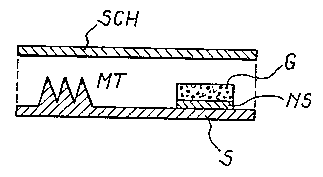
Fig. 7 is a doss-section view of a field emitter display (FED)
according to the invention, without the "tail", wherein an insulating
substrate
S and a porous layer of NEG (G) are separated by a metallic fixing strip NS.
The following example is merely given for an explanatory purpose and
does not limit in any way the spirit and the scope of the invention.
EXAMPLE
150 g of Titanium hydride, having a particle size lower than 60 um,
were introduced, together with 50 cc of demineralized water, in the steel
container of a planetary ball mill.
After the natural evaporation of The water, a powder of titanium
hydride having a particle size lower than 20 um (average size: 3-5 um) was
obtained by adjusting the time (about 4 hours) and the milling speed and
after the fixing of a suitable number and size combination of the balls in
said
container. The surface area was 8,35 m2lg.
WO 95!23425 PCTI11'95/00031
.; X1.14962
-10-
150 g of St 101 alloy (84% Zr, 16°!° AI), having a particle size
lower
than 53 um, were milled at the same conditions and with the same
parameters used for milling the titanium hydride; a powder consisting of
particles having a size lower than 30 um (average size. 8-19 ym) was thus
obtained. The surface area was 2,06 m~lg.
Subsequently, in a plastic bottle, 70 g of said milled titanium hydride
were mixed with 30 g of said St 101 alloy, finely milled. These are the
typical
proportions for forming a composite Better material called St 121. Then,
there were added 150 cc of suspending means obtained by mixing 300 cc of
isobutyl acetate, 420 cc of isobutyl alcohol and 5,3 g of collodion cotton
(nitrocellulose). The bottle was then sealed and mechanically shaken for a
time longer than 4 hours.
There has been thus obtained a homogeneous suspension which, if
stored for any period, must be shaken again for about two hours before
being used.
The suspension was then deposited on the surface of a metallic
support by means of a spray system comprising a plastic tank, a pressure-
regulated spray needle-valve (model 780S Spray Valve of the EFD
company) and a control unit (model Valvemate 7040 by EFD).
For the present example there were used metallic supports made of
Ni-Cr, strip-shaped, 0,05 mm thick and 4 mm wide (in other tests sheets 0,02
mm thick have been used).
The valve was supported by a pole so that the spraying nozzle was
about 30 cm away from the horizontal surface of the support. The depositing
process comprised a sequence of steps (cycles) wherein the valve was
opened for a second approximately, thereby letting the suspension flow as
tiny droplets, and then closed for a period of 15 seconds approximately,
wherein the suspension means could evaporate. In order to accelerate the
latter process, the support was kept at about 30° C by means of a
heating
support plate.
The thickness of the deposit of Better material was proportional to the
number of spraying cycles.
The samples coated by a St 121 powder on one face only, were
introduced into a vacuum oven, wherein the pressure was reduced to less
than 10'~ mbar; the temperature was then increased up to approximately
450° C, value kept for about 15 minutes.
R'O 95/23425 . a i~ PCTlIT95100031
r 217962
-11-
'8-hereafter, the temperature of the oven was increased up to 900° C
(sintering temperature) and kept for 30 minutes.
Finally, the system was cooled down to the ambient temperature and
the coated supports were extracted from the oven; the deposit of sintered
powder was 150 to 180 pm thick along the surface of the metallic support.
Fig. 1 and 2 are the micrographies obtained from the SEM (Scanning
Electron Microscopy) analysis of the visible surface of the Better material
deposit after being sintered.
Fig. 1, i.e. the 1000x enlarged micrography of a visible surface portion
of the Better material layer obtained according to example 1, clearly shows
the high porosity and the good sintering level of the sample.
Fig. 2, i.e. the 1860x enlarged micrography (by backscattering
analysis) of a portion of the cross-section of the same Better material layer
of
the example (A-A section in Fig. 4), points out not only the good layer
porosity, but also the satisfying uniformity of the distribution of the
sintered
mixture components, as well as the good fixing to the Ni-Cr substrate.
Fig. 3 (line 1 ) reports the carbon monoxide sorption tests.