Note : Les descriptions sont présentées dans la langue officielle dans laquelle elles ont été soumises.
Wo 95114306 ~ 2 ¦ 7 6 3 3 7 PcTlus94ll3l64
,
PULSED lONJ~E~'~q ~OURCE .
This invention relates generaUy to apparatus for producing ion beams. More
h,~ ly it relates to v ' 7l~-conf ned anode plasma (MAP) ion sources. Still
more particularly, it relates to such MAl? ion sources as are designed to produce minimum
ion beam rotation amd precise control over the ion species present in the beam.
B~ Frourld
A variety of ion beam sources exist. MAP ion sources are particularly interesting
because of their ability to shield the ion source structure from the destructive effects of the
ion plasma by the magnetic shielding created by the magnetic structure of the MA3' ion
source
~ owever, most of the prior art MAP ion sources were designed to used in a beam
line that also included ~ . . . , steering and f,J ~. . . t of tbe produced ion bearns by
varjous electric and/or magnetic fields. Ihis steering and ~, ,.,.'. .. ,1 was necesSary
bccause of the beam rotation created by the ma~netic structure of these MAP ion sources
whjch imparted slgnificant rotation to the produced ion beam. The downstream electric
and/or magnetic fields add complexity, si~e and expense to a system emp~oying such MAP
ion sources.
~ n cx&mple of suc~l a prior arr l~qAP ion bean~ source, often cal~ed an ion diode, is
~ound j~ a p~perb~tllein~entoroft~lc~resfmin~enrion, Greenl~,J.B e~a~.,"P~asma-
SUBSTITUTE SHEET (RULE 26~
WO95/14306 ~ ~ ~1 76337 PCrlUS94113164
Anode lon Diodc Researcil al Corncll: Repetit;ve-puise, and 0 1 T~ Single Pulse
Experiments," Proceedings '`th International Conf on Higi~-Power Particle Beams, pp.
199-206, Novosibinsl~, USS ~, July, 1990. The RRlD ion diode described therein bears
some similarity to the present invention, but its magnetic design is such that substanlial
beam rotation is imparted to the produced ion beam.
It would be desirable to reduce or eliminate the need for such duw~
apparatus by designing a new MAP ion source that had minimal or no beam rotation as a
result of the creation and ~Ifr .l~-ratif~n of the ion beam by the ion beam source
MAP ion beam sources have a variety of uses. The most obvious is use in
;ul~dl ion ' . ' ' processes. However, a need for a capability to do surface
treatments to large areas of various materials with high power, short pulse ion beams has
arisen that required a new type of MAP ion bearn source Witil mir~imai or no beam rotation
and precise control over tiqe ion species used. The use of surfiu;e treabnents to improve
properties such as surface hardness, wear resistance, corrosion resistance, and fatigue
i.tfetime add signiicant vaiue to a wide range of products in industries including
automobile ~ ~" aerospace, I ' u~ , ' , tool and die r ' ~ power
generation, and the production of steel, aluminum, ceramics, and plastics. This unmet
need was the impetus for the creation of the invention disclosed herein.
Aithough experiments with prior art ion diode sources have indicated that ion
beams might be useful for t lese sort of surface treatments, no commerciai
~ ' ' have resul~ed. The use of ion beams for thermally aitering the near
surface . ~ rl i~ of a material has been fraught with substantiai problems. Mostnotabie ofthe ~imitations with existing ion beam t~nhnnl~;h c have been: I) high costs per
area treated; 2) the inability to generate a large number of pulses without the costl~
I~lJld.,~ of ion beam generator UU~ Joll~ , 3) low repetition rates, 4) low average
power; and 5) the inability to reliably produce a uniform ion beam of a single selectable ion
species.
Typical ion beanl _enerators use dielectric surface arcing on an anode as a source
of ions ~lld ~ rcarl~r ma~ e~ical!! ()r gcomclrlcall~ direct and ~ocus t~le ~enerated io~l
bealll onlo li~e Illàicriâ' c~ i;crc~ lis surrac~ arcill~ (also ca~led "fiasho~ er") dcslro~ s
SUBSTITUTE SHEET (RULE 26)
WO 95/lf306 3 2 1 7 6 3 ~ ~ PCT/IJS94/13164
tllc anodc surfacc in lcss ~I~all 100 pulscs, and produces a mixed sDccies of iolls tllat cam~o~
be adjusted. Other difficulties arising from flashovcr include: production of large
quantities of neutral gas trat mal~es high repetition rate difficult, generation of dcbris
~vhicll can ~t~nt~min,tte. surfaces being treated, and non-uniformity and irreproducibilily of
tlle beam in somc cases due to ti~e localized and difficult to control nature offiasllover, as
well as the detrimental beam rotation discussed above.
State-of-the-art ion beam generators are typically "one shot" devices, i.e., they
operate at low repetition rates (<C I Hz) Existung ion beam generators cannot beoperated at high repetition rates ~ I Hz) for a number of reasons. First, existing pulsed
power supplies are not abie to generate electricai pulses at high repetition rates having the
voltage, pulse width ~I.e., nontinai temporai duration), and power required to generate the
ion beams needed ~I.e consistent with the discussion above) for the various beneficiai
.~; ' described herein. ~rhis iimitation renders ,.~ i: . ' impracticai.
~Iowever, it should be noted that one shot surface treattnents from a robust ion beam
source are useful m some ~ Second, the design of existing ion beam generators
does not ailow repetitive operation for an extended number of operating cycles ( 10 ')
without~ la.~ of major~ . t.. 1~ Thislimitationwouldre~iuirea,.. ~ t, ._.l~J-
time - ~ ur~lt~lul;llg time ratio i~ with routine .. ,i~ lg operations.
Third, existing ion beam generators generaily operate with electricai efficiencies < 5%,
thus presenting major challenges to the pulsed power supply and the cooiing system of the
generator. These limitations and others have made it impossible to routinely utilize the ion
beam technology described above for surface treating materials.
Summar~ of the Invçntion
The present invention provides a ne~ type of magnetically-coniined anode plasma
ion beam source. The new ~AP ion diode has improvements in a number of areaS Itsmagnetic fields are designed to ha~e a profile such that tlle separatrix (B=0) be[ween the
fast coil iield and tlle slo~ coil field is located llear the anode to minimize or eliminate ion
bçam rotalion. Tl~ las nozzle 1~ desi~ned io prod~lce a hi-gh mach number (supersonic)
~as ilo~ raie lO ef}icien~ lo~z!i. e tlle (æs pui~ troduced into tlle ionizin., reg~ion
SUBSTITUTE SHEET ~RULE 26)
WO 95/14306 ~ 7 6 3 3 7 PCT/US94/13164
4 ~
proxinlate Ihe fast coil. Means are also provided io create an adjustable bias field to
control the formation posit on o~the plasrna. A fast ringing field is imposed on the gas
puff as it is delivered to t~l~ ionizing region to pre-;onize the gas. These and other
improvements contribute to the MAP ion beam so~rce of this invention.
The use of the MAP ion diode of this invention for large scale surface treatmentprocesses requires a pulsed bigh power source. Some of the detailed description below
will be deYoted to one such source, the Repetitive High Energy Pulsed Power (RFfEPP)
system developed at Sandia National I ahor~ ri. ~ For single shot ., ' other
power sources such as Marx generators could aiso be used.
Further detail concerning the present invention and its scope wili become apparent
from the detaiied discussioii of specific ' - ' presented below However, it
should be understood that the detaiied desc iption and specrfic e~tnples, while
, the class of ~ l ~ of the invention arld its uses, are given by way of
illustration only, since various changes and ~ within the spriit and scope of the
;nventio illbeapm~tt~_eshddintilcan~;omtldsdetddd/!scdp~ior
5U3STITUTE SHEET(~ULE 26)
WO 95~14306 ~ t~ T 7 6 3 3 7 PCTIUS94113164
Brief Oescriptioll of the Drawinos
~ he present invention ~vi11 become more f~lly understood from the detailed
descrip~ ion given llereinbelo~ and t}le ~Co~ J~illy;llg drawings which are given by ~ a) Or
illustration only, and tllus are not limitatiYc ofthe present invention, and wherein:
Flgure I is a schematic ofthe RHEPP pulsed power system;
Figure IA is a circuit diagram of a puise Culll~llea:~loll system 15 utiiized in the
pulsed power system of Figure l;
Figure IB is a cross secionai view of a pulse forming Cne element;
Figure I C is a cross sectionai view of the Linear Inductive Voltage Adder (LIVA);
Fif~ure 2 is a partial cross sectionai view ofthe ~ "~ confmed ;mode
plasma (~AP) source 2'i ofthe present inYentiOn;
Figure 2A is a modified version of F~gure 2 showing the magnetic field iines
produced by the fast arld slow coiis in the MAP source;
Fgure 2B is an expanded view of a portion of Flg. 2 showr~g the gas irliet vaiveand the gas irl`iet ch~mnel;
Figure 2C is a schematic diagram ofthe electric circuit for the fast coil; and
Figu~ e 3 i a s~hema ic ~Ull cro~seclioral wew o~the M~F ion dlode
SUBSTITUTE SHEET (RULE 26)
WO 95/14306 - ~ ~ 6 ~ t 7 6 3 3 7 PCTIUSg4/13~64 ~
Detailcd Description Qfthe In~ention
The following discussion is a description of one system which can be utilized toproduce the ion beams for surface treatment of various materials. This system has two
major subsystemsl tile puls ld power source ard tl1e MAP ion diode.
The MAP ion diode which for~ns the present invention, when combined with the
RHEPP source, provides for an ion beam generator system capable of high average power
and repetitive operation over an extended number of operating cycles for treating large
surface areas of matelia~s at WllllllW' "~, attractive costs. In particular, the ion beam
generator of the present invention can produce high average power (IkW4MW) pulsed
ion beams at 0.1-2.5 MeV energies and pulse durations or lengths of from about 10
,~ (ns) - 2 ~ s) or longer as necessary for the particu~ar
application. The ion beam -~enerator can directly deposit energy in the top 50 u..._t~
(llm) of the surface of a ma;elial. The depth of treatment can be controlled by varying the
ion energy and species as well as the pulse length. The MAP ion diode can be combrned
with other power sources where less demanding power demands are present.
The f rst of the . A ~ ' ' C in the pulsed ion beam generating system is a compact,
electrically efficient, repetitively pulsed, ~..~.._t;~ switched, pulsed power system
capable of lO9 pulse operating cycles ofthe type described by H. C. Harjes, et al, Pro 8th
IEEE Int. Pulsed Power Conference (1991), and D. L. Johnson et al.7 "Results of Initlal
Testing of the Four Stage RHEPP Accelerator" pp. 437~40 and C. HarJes et al.,
"('ho~n n ri7~ion of the RE~PP I 1lS Magnetic Pulse Compression Module", pp. 787-
790, both reprinted in the Digest of Technical Papers of the Nmth IEEE T, .l, . .~
Pulsed Power Conference, June, 1993, all of which is ;..~,u, I,u, dLed by reference herein.
These references in conjunction with the discussion herein below place fabrication of such
a pulsed power source within the sldll ûf the art.
A blocl~ diagram of a power s~ stem produced according to the teachings of the
preselll application is shown in Figure 1. From Ille prime po~ver input, several stages of
magnetic pulse compression and volla~e addilion are used to deliver a pulsed po~er signal
of U~l to ~.5 l~q~r Gû ns F\~'~q. '2.9 kJ p~llses at 3 ratc of 120 ~ to an ion bcam source
SUBSTITUTE SHEET (RULE 26)
. 2
wo gs/l4306 7 1 7 6 3 3 7 PCT/US94)1316-t
ror tllis panicular system. Tl-e po~cr s}~stell1 converts AC power from the local po~er
grid into a form that can be used b~ an ion beam source 25.
Referring to rigure l, in one ~ of t~le invention, the power system
compnses a motor 5 wllich drives an alternalor 10. The altemator 10 delivers a signal to a
pulse UUIII,~ X~;UII system ~ 5 which has two subsystems, a I Its pulse compressor 12 and a
pulse forming line 14. The pulse l,.,,,lt,,~;o,~ system 15 provides pulses to a linear
inductive voltage adder (LIVA) 20 which delivers the pulses to the ion beam source 25
The altemator 10 according to one ~ ' is a 600 kW, 120 Hz alternator. In
the unipolar mode, it provides 210 A mms at a voltage of 3200 V rms with a power factor
of 0.88 to the magnetic switch pulse compressor systent 15. The alternator is driven by a
motor conrlected to the local 480V power f~rid. The particular alternator used herein was
designed by ~ ~' Corporation and fabricated at the Sandia National T ~I~nr~tnr;~im Albuquerque, New Mexico. It is der~ribed in detail in a paper by R M. Calfo et al.,
"Design and Test of a Continuous Duty Pulsed AC GeneratoP in the ~IU~i..o~ of the
8th IEE~ Pulsed Power Conference, pp. 715-7187 June, 1991, San Diego, CaGfornia.Tt:tis reference is ~ IJu~ ed herein in its entirety. This particular power system was
selected amd built because of its relative ease in adaptabiGty to a variety of loads. Other
power sources may be used and may indeed be better optirr~ized to this particular use. For
example, a power supply of the type available for Magna-Arnp, Inc. comprising a series of
step-up l, . . . r " .. . ~ connected to the local power grid feeding through a suitably-sized
rectifier could be used. The present system however has been built and performs
reasonably well.
In one ~,.lllJ. ' ~, the pulse ~ulll~ iOll system 15 is separated into two
subsystems, one of which is a common magnetic pulse compressor 12 composed of a
plurality of stages of magnetic switches (i.e., saturable reactors) the operation of which is
well known to those skilled in the art. This subsystem is shown in more detail in Fig. IA
The basic operation of each of tlle stages is to compress the time width (transfer time) of
and to increase the amplitude of the volta_e pulse received from the preceeding stage.
Since tllese are ~er~ lo~ loss s~itclles relati\~el!~ little of the po~er is wasted as ~leal, and
1le enero~ in each pulse decreases relati~ el! Iilt~e as it moves from sta~e to stage. The
SUBSTITUTE SHEET(RULE 26)
WO 95114306 ' ' Z ~ 7 6 3 3 7 pcr/usg4/l3l64
sl~ccific subs)~stem uscd 's~erein is described isl detail b~ H. C. Harjes, et al.,
"Characterization of the RHEPP I S,lS Magnetic Pulse Compression Module", 9th IEEE
Internatiollal Pulsed Po~er Conference, pp. 7~7-790, Albuquerque, ~rM, June, 1993.
Tslis paper is incorporated by reference herein in its entirety. These stages as developed
for tllis system are quite lar e. In tlle interest of conserving space, it would be possible to
replace the first few stages ~vith ~SJkll~ designed silicon control rectifiers (SCR's)
to acwmplish the same pulse Wl~ a~lUII result.
These stages 12 convert the output of the altemator 10 into a I ~ts wide LC charge
waveform which is then del vered to a second subsystem 14 comprising a pulse forming
line (PFL) element set up in a voltage doub ing Blum'~ein, r~ The PFL is a
triaxial water insulated Gne that converts the input LC charge waveform to a flat-top
trapezoida'. pulse with a design 15 rss rise/fa~l time and a 60 rls FW~ The ~
and operation of this e~ement is descr'sbed in detai. by D. L. 30h}tson et a'. ~csults of
Initial Testing of the Four tage REIEPP Accelerator", 9th IEEE T ' ' ~ Pu',sed
Power Conference, pp.437-44û, ~l' , . , NM, June, 1993 This paper is a~so
l~w~ ,uo. cltd by reference itt its entirety. A cross sectiona's view of the PFL is shown in
Figure IB.
The pulse WlllsJltaa u-- system 15 can provide unipolar, 250 cV, 15 ns rise time,
60 ns full width ha'f maximum (FWHI~, 4 I;J puises, at a rate of 120 Hz, to the linear
inductive voltage adder (LIVA) (2û). In a preferred ~ 1 '' t, the pulse . ~a;
system 15 should desirably have an efficiency >$û% and be composed of high reliability
. U~ with very lu~ ;-r '' (~IOJ-10~ pulses). Magnetic switches are preferably
used in all of the pulse ~ . caa;UII stages, MS I -MS5, beQuse they can handle very high
pea~ powers (i.e., high voltages and currents), and because they are basiQlly solid state
devices with a long service if e. The five wl~ caa;ull stages used in this ~mhf ' as
~vell as the PFL 14 are sho~n in Flg. I A. The power is supplied to the pulse cd-l-l~l caa;UI~
s~stem 1~ from the alternat3r 10 alld is passed through t~le magnetic switches, MS I -MS5,
lo t~le PFL 1~. T~le PFL is connected to the linear inductiol1 voltage adder (LIVA) 2û
de~crib~d belo~. Tlle second ard t~lird ma<~n~iic s~ ches, MS2 and MS3, are separated
b~! a s~e}~-ul~ Iransformer Tl as sho~vn 5~ C~I MS~) is all inversion switch for the PFL.
SUBSTITUTE SHEET (RULE 26)
~ r ~ 2 1 7 6 3 3 7
WO9~/14306 ~ - : 9 PCT/IIS94~13164
e pulse form;ng linc (PFL) element ~ 4 is silo~n in c. l ,....,.l ;..,.lly in Fig. I A and
illcrosssectioninFig. IB. MS6inFig. lAuu~ u~ totileinversionswitch302
sllo~nillFig. IBlocatedont~leinputsidcoftiletri-axialsection314OftllePFL. Outputs~vitcl~es 304 and charging cores 306 are also shown. The regions 310 are filled with
deionized ~vater as the dielectric. The interior region 30S is filied with air and oil coiling
lines, not shown, for the output switches 304. The output of the PFL is fed in parallel to
each of the individual LIVA stages 20, with the positive connponent flowing through
conductors 316 and the shell 318 of the PFL serving as ground. The positive conductors
316 are connected to each oftile LIVA stages.
The LIVA (20) is preferably iiquid dielectric insuiated It is connected to tbe
output ofthe PFL and can be oonfigured in different numbers of stages to acbieve the
desired voltage for delivery to the ion beam source The LIVA20 can deiiver nominal 2.5
MV, 2.9 W, puises at a rate of 120 Hz to tite ion beam source 25 wher~ configured with 10
stages of 250 kV each. For most of the ion beam treatmentr" the LIVA was configured
with four stages of 250 kV each, such tbat the LIVA delivered a totai of 1.0 MV to the
ion beam source. However, this voltage.can be increased or decreased by ch<mging the
number of stages in the LIVA to match the particular materiai processing need. The
nominai output pulse ofthe LIVA 20 is the same as that provided to it by the PFL,
namely, trapezoidai with 15 ns rise and fail times and 60 ns FWHM (fiull width half
maximum). Fgure IC shows a cross section ofthe four stage LIVA The four stages,
320, 322, 324, and 326, are stacked as shown and fed the positive pulses from the PFL via
the cables 321, 323, 325, and 327. The stages are separated by gaps 330 and surrounded
by ~ rul ll,." oil for cooling. The output from each of the LIVA stages adds to deliver a
single total pulse to the ion beam source sl~o~n here ~. h- ~ aE 25 which is located
~vithin a vacuum chamber 3i2, shown in part;al view. As with the PFL, the outside shell
ûf the LIVA is connected to ground
T~le power system P (Figure 1) as described, can operate uu~ uu:,ly at a pu~se
rcpetition rate of 120 Hz delivering up lo 2.5 W of energ~ per pulse in 60 ns pu~ses. The
speciiic po~ er s~stel~l described llere can deli~ er pulsed po~er signals of about 20-1 ûOû
n~ du:-atio~ i] ion beam eneroies of d.'~-~.5 I~qe~ . The power system can operale a~
SUBSTITUTE SHEET(RULE 26)
W095114306 ~ ~ 1 0 ~ 76337 PCr/US94~13l6
50~ elcctrical efficienc y fiol~ c ~all plug to encrgy dclivered to a matc~-ed load. The
po~ver s~stem P uses lo~v loss pulse uu~ a5;u~l star~es il~cul,,uld~ g, for example, low
loss ma~netic material and solid state compollents, to convert AC power tO short, high
voltage pulses.
T~e abilit~ to produce voltages from 250 liV to several MV by stacking voltage
using a plurality of ;nductive adders incorporating low loss magnetic material is a principle
feature when high voltages are needed, although it is also possible to use a single stage
pulse supply, eGminating the need for the adder.
The power system can operate at relatively low impedances (< IOOQ) which also
sets it apart from many othe- repetitive, power supply Ir~ }....~ r C~ such as ibased systems. This r~u~ . high treatment tates and the treatment of large areas (5
to more than lOOû cm2) with a single pulse so as to reduce edge effects occurring at the
transition between treated and untreated areas.
The second component ofthe pulsed ion beam system is the MAP ion beam source
25, the invention herein (shown in Figure 2). The MAP ion beam source is capable of
operating repetitively and ef iciently to utilize the pulsed power signal from the power
system efficiently to turn gas phase molecules into a high energy pulsed ion beam. It can
also be operated in the single shot mode, as necessary for a particular application. A
precursor of the ion beam sTrce is an ion diode described generally by J. B. Greenly et al,
"Plasma Anode Ion Diode Research at Comell: Repetitive Pulse and 0.1 TW Single Pulse
E~ , PI u~,c~u~s~ c f 8th Intl. Conf. on High Power Particle Beams (l 990) all of
which is ;llwl~Juld~e~ by reference herein. Although this reference ion diode differs
s;~.uG~lllly from the ion diode utiliæd in the present system as discussed above, the
baclcground discussion in this reference is of interest.
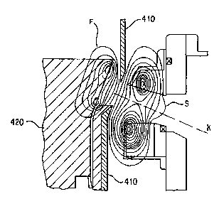
The ion beam source 25, according to the principles of the present invention, issllo-vn in Figure 2. The ion beam source 25 is a ll,d~ -confined anode plasma
(MAP) source. Figure 2 is a partial cross-sectional view of one symmetric side of the ion
bcam or l~AP source 75 The ion beam or MAP source 25 produces an annular ion beam
ic~i can be brout~ to a lroad focus s!~mn)e~ric about the a~is X-X 400 shou~n. In
t~lc c~.t~ode electrode asscm l~ 30 slo~ lS risc tilll~) ma<~netic ficld c ~ils 414 produce
' UBSTITUTE SHEET (RULE 26)
WO 95/14306 ` ~ 2 1 7 6 3 3 7 PCTlltS94113164
agnctic f u~; S (as sllo~vn in Fi~ '2A) ~ icil i~rovides tlle ma5nctic insulation of the
acceleratinæ æap bet~veen tlle cathodes 412 and the anodes 410. The anode e~ectrodes 410
Qlso act as 12lagnetic f ux sllapcl ~ The slou~ coils 414 arc cooled by adjacent ~ater lines,
not silo~n, incorporated inlO tlle structure 30 supporting the cathodes 412 and the slou
coils 414. T~le main portion of the MAP structure sllo~vn in this Figure is about 1 S cm
high and ~vide. The complete MAP ion diode can be visualized as the revolution of the
cross-sectional detail of Fig. 2 about the oentral axis 400 of the device to form a
cylindricai apparatus. A full cross sectional view appears in Fig. 3.
The ion beam or i~AP source 25 operates in the follo~ving fashion: a fast gas
valve assembly 404 located in the anode assentbly 35 produces a rapid (200ils) gas puff
which is delivered through a supersonic nozzle 406 to produce a higbiy locaiized volume
of gas directly in front of the surface of a fast driving coil 408 located irl an insulating
structure 420. The nQzzle is designed to prevent any transverse 'dow of non-ionized gas
into the gap between the anodes 410 and cathodes 412. After pre-ionr~ing the gas with a
I ms induced electric field, the fast driving coil 408 is fuily energized from the fast
capacitor 150, inducing a loop voltage of 20 kV on the gas volume, driving a breakdov~n
to full ionization, and moving the resuiting plasma toward the anode electrodes 410 in
about 1.5 ,us or less, to form a thin l.l~,l~.i~,.,lly-confined plasma layer. The plasma
Illu~ L~l;ly stagnates at this B=0 region~ the separatrix, next to the insulating field S
produced by the slow coils 414, awaiting the delivery of the main r ~~~1 " ~ positive
electricai pulse to be delivered at the a2,0des 410 from the LIVA discussed above.
The pre-ionization step is a departure from the eariier MAP reference which
showed a separate conductor located on the face of a surface ~ull~ u,.lil~g to the
insulatino structure 420 herein. Since this conductor was exposed to the plasma, it broke
do~vn frequently. The inventor herein discovered that the separate pre-ionizing structure
~as ul~e~.e:,3.1~y. The gas can be effectively pre-ionized by placing a small ringing
capacitor 160 in paraliel with the fast coil. The field oscillations produced by this ringing
circuit pre-ionizc the ~as in front of t~2e anode fast coil A schematic electrical diagram of
this circuil is sllo~n in Fi'l. 2C.
SUBSTITUTE SHEET(RULE 26)
Wo 95/14306 ~ 1 2 ~ ~ 7 ~ 3 3 7 PCTNSg4~13164
I have also disco ~ered 1~ )rior tO ~ro~ isiol of tlle main pulse to tlle fast coi~ i;
is beneficial to have ti e abilil~ to adjusl tl e configuration of t~le magnetic field in the gap
be~ een tlle fast coil alld tlle anode lo adjusl t~e inilial position of p~asma formation ill tlle
puffed gas pulse prior to t~le pre-iollization sle~ This is ~ hrd by the provision of
a slo ~ bias capacitor 180 and a protection circuil both being installed in parallei with the
fast coil and isolated therefrom b~ a controllable s~vitch S2. A slow bias field is thus
created prior to pre-ionizatir n of the gas by the fast coil. This circuit is also shown in Fig
2C.
In further explanation of the electrical circuit for the fast coil as shov~n in Fig. 2C
the bias field capacitor 180 c rives a greater than I l~ivlua~d risetime current in the fast
coil before the main capacitor pulse begins. This allows adjustrnent ofthe fieldr S~ produced by the fast capacitor current. The fast capacitor 15û drives a I
risetime pulse in the fast coil. The preionizer capacitor 160 causes the
volhge across the fast coil to ring with a much less than -I ...~.1 period~7 inducing a
large oscillat;ng electric Sel~ in the gas to be ionized leading to partial ionization of the
gas. The rising magnetic fie d produced by the fast coil 408 pushes the ionized gas away
from the fast coil stagnating it against the preexisting magnetic field from the slow coil
414.
After pre-ionization the fast coll is then fully energized as described above tocompletely breakdown the gas into the plasma. After this pulse the field collapses back
into the fast coil which is co mected to a resistive load which is in tum connected to a heat
sink not shown. In the present ~-llbod;..~ L cooling channels in the supporting structure
are used but other solutions are possible and relatively all d~ rul w .. l. In this manner
heat build up in the fast coil s avoided.
The fast coils 408 have been redesigned from the reference fast coils in several~a)s as ~ell as the heat sinl;ing mentioned above. The gap between the fast coil and the
anode electrodes 410 llas be n reduced ~ith th~ result t~lat the amount of necessar~
maglletic energy has been decrcased b~ o ~er 5Q%. The lo~ver energy le~u; ~ permits
rcpctiti~c us~ at hio~ler frequencie~ ~.nd reduce;~ the comple~:it~ ofthe feed s~stem ~olta -es
SUBSTITUTE SHEET (RULE 26)
WO95/14306 ~ , i, .~ 1 3 PCrfUS94113164
~fortilcfas;coils. Tlledcsif~llofti~clle~ fuY-sllapi~lganodcclecrodeasselllbl~hasalso
contributed to these beDeficial resul~s.
Ti~c l~lscd po~cr sl_nal fronl tllc l~ower s~stelll is then applled ~o the anodeasselllbl~ , accelcraling ions fron~ tilc plasllla to form al~ ion ~eam ~;. The slo~v (S) and
fast (F) magne~ic fux slructures at t1~c lime of ion bealll extraction, are shown in Figure
2A. T~le definite separation bet~veen ~he fux from the fast coil firom the Qux from the
slow coil is shown therein. This is ~ l - ;i by the flux-shaping effects of the anodes
410 and a~so b~ the absence of a slow coil iocated in the insulating structure 420 as was
taught in the earlier MAP reference paper. The slow coils in the present MAP ion diode
are located oniy in the cathode area ofthe MAI?. This anode ~dux shaping in, ; ~with the location of slow coiis in the cathode assembly is different from that shown in the
MAlP reference paper and pennits the high repetition r tte, sustained operation of the MAl?
diode disclosed herein This design aiiows the B=0 point (the separatrix) to he positioned
near the anode surface, resulting in an extracted ion beam with minimai or no rottttion.
This minimai rotation is necessary for effective deliveJy of the be~tm to the materiai to be
treated.
Figure 2B is a detaile~i view of the gas valve assembly 404 and the passage 425
which conducts the gas from the val~e 404 to the area in firont of the fast coil 408. The
passage 425 has been carefuliy designed to deposit the gas rn the locaiized area of the fast
coii with a minjmum of blow-by past this region. The details of the cross sections of the
passage 425 were designed for supersonic transport of the gas puff. The design was done
with readily available gas flow computer programs and is within the skill in the art. The
gas valve flapper 426 is operated by a small magnetic coil 428 which opens and closes the
flapper 426 upon actuation from the MAP control system. The flap~er valve is pivoted on
the bottom end 427 of the flapper. The coil 428 is mounted in a high thcrmal conductivit~
ceramic support slruCture 429 which is in turn hea~ sin}~ed to other structure, not shown
Alternativel~, externally coole(f ~vires surrounding the coil could also serve to extract the
lleat from tile coils. This heat siniiillg is necessary for the sustained operating capability of
tilC l\g.~l'. I ile g2~ is de,i~ ered IO tl~ ali c fi om a plcnum 431 be~und t~le base of tile
SUBSTITUTE SHEET (RULE 26)
. ~ . r ~
WO 9S/14306 1 4 ~ 1 7 ~ 3 3 7 PCT/USg4/13164
. J~
flapper. The ~le~ 4, ~ s lould bc ~ i~u2iize~i as bein<~ connected IO a larger plenu~
localed at t~le central core of tlle coml~lele l\~AP ion diode as shown in Fig. 3 .
T~le ~acuum in tlle .loZ ic 4Q(` ra~idl~ ~ra~s the gas into the MAP once tl~e flappe
42v is opencd Tlle function of ll~e llozzle is to producc a direaed flo~Y of gas onl~ in the
direction of flo~ and not tra~ls~ erse IO il. Such transverse flow would direct gas into the
gap between the anode and t~le cat~ode w~licll would produce detnmental arcing and other
effects. The reduction of the fast co;l-anode gap discussed above makes the design of the
noz~le very important to the successful operation of the MAP. Fortunately, gas flow
design tools are avaiiable ald were used to deveiop a no~zie with improved gas flow
(}ugher mach number) and minimal boundary effects. This improved nozzie has an
enlarged opening into the ~ap between the fast coil and the near edge of the anode which
tapers from 9 to 15 mm instead of the straight walied 6 mm conduit in the reference MA3'.
The operating pressure of the gas in the puffvaive has been inr,reased from the range of 5-
25 psig to the range of 2540 psig. Experiments have corhirmed much improved MAP
operation as a result of this new design.
The ion diode of th s in~ention is distiguished from prior art ion diodes in severai
ways. Due to its low gas load per puise~ the vacuum recover,v within the MAP allows
sustained operation up to and above ~ 00 Hz. As discussed above, the magnetic geometry
t ~ different from previous ion diodes. Prior diodes produced rotating beams
that were intended for A~ in which the ion beam propogates in a strong aA~ial
magnetic field after being generated in the diode. The present system re~iuires that the ion
beam be extraaed from the diode to propogate in field-free space a minimum distance of
20-30 cm to a material surace. The magnetic cu~ ul ~L;v..~ of previous ion diodes are
incapable of this type of oFeralioll because those ion beams were forced by the geometries
of those diodes to cross net magnetic llux and thus rotate. Such beams would rapidly
disperse and be useless for the present purposes. B)~ moving the slow coils (the diode
insulatin, magnetic fiela coils) to tlle calllode side~of the diode gap eliminated the
n~agnetic field crossing for tlle b~alll bul required a total redesign ofthe magnetic syste
for t~le allode ~asma so~rc~.
S JBSTITUTE SHEET (RULE 26)
21 7~337
WO9~/14306 1 5 PCTII~S94/13164
Tl~c mo~lifi~ion~ tQ tlle ra~l CO!I disc-lsscd abo~ e rcsult ill an energy rcquircment
t~lat is 5-10 times less tllan previous confiouratio~ls The l~ include: the
elimination of a slo~ coil on Illc allode side of tlle diode and its associaled feeds, beltcr
control over tlle ma~netic field s11dpi~ alld con~act of thc anode plasma to t~le anode
eleclrode structure through use oLtll~ partiall~ ficld-penetrable electrodes, the elimination
of the separate pre-ionizer coil fro~n the prior ion diodes, the circuit associated with the
fast coil to provide "bias" current to adjust the magnetic field to place the anode plasma
surface on the correct flux surface to eliminate beam rotation and allow optimal,UlU~ g~l~;Ull and focusing ûf the beam, and the redesign of the gas nûzzie to better
locaiize the gas puffwhich enables the fast coil to be located close to the diûde gap which
in turn reduces the energy I ~tu;ll and complexity of the fast coi~ driver.
The plasma can be formed using a variety of gas phase mûlecules. The system can
use any gas ~mcluding hydrogen, helium, oxygen, nitrogen fluorine, neo4 chlorine and
argon) or vaporizable liquid or metal ~mcluding lithium, beryllium, boron, carbon, sodiùm,
~ n~C;llm, aluminum, silicon, I ' . ' uu~, sulfur, and potassium ) to produce a pure
source of ions without cons~tming or damaging any compûnent other than the gas supplied
to the source. The ion beam K propagates 20-30 cm in vacuum (~10 3) to a broad focal
area (up to 1000 cm~) at the target plane 195, shûv~n in Fig. 3, where material samples are
placed for treatment and can therrnally aiter areas from 5 cm2 to over 10û0 cm2.The iûn beam or MAP source 25 is capable of operating at repetitive pulse rates of
100 Hz uùlllilluuu~ly with long component lifetimes >106. The ion beam or MAP source
25, according to the principles of the present invention, draws ions from a plasma anode
rather than a soiid dielectric surface flashover anode used in present single pulse ion beam
sources. Use of a f as~lover anode typically introduces a variety of ~ to the
surface of the material, often willl detrimental results. One of the significant advantages of
tlle using the improved MAP source disclosed herein is that one has precise control over
the componems in the ion beam b! con~rolling t~le composition of the gas source.
SUB5TITUTE SHEET (RULE 26)