Note : Les descriptions sont présentées dans la langue officielle dans laquelle elles ont été soumises.
2~ 7~nsl
Wo 96/10845 r~.,lL,~ ,,,
S~ device cnmrriqirl~ a ~.lu..I..Ll;. memory element with a lûwer electrûde
prûvided with am ûxygen barrier.
The inventiûn relates to a ' device ~ Y, a
... body with a c ~; h 1~ JI element Cnmrricing an Cl..,LIiu~-lly conducting
region on which a capacitor forming a memory element is present with a lower electrode,
and oxidic f..lu..~ , dielectric, and an upper electrode, which lower electrode makes
5 electrical contact with the conducting regiûn and comprises a layer with a cûnductive metal
oxide and a layer c~ platinum. The mvention also relates to a method of
" ,.,r~. l...;,.~ such a ~...,;..,...l... l.,, device.
The memory element mentioned above, fûrmed by a capacitor with a
f~"lu.lc~llil, material as the dielectric, is a Don-volatile memory element. When a voltage is
10 applied across the capacitor and removed again - in other words, a voltage pulse is applied -
a remanent p~ ;---- will be present in the f~ u-l-,~LIiC material. When an equally large
voltage pulse of opposite polarity is applied across the capacitor, the remanent po' is
reversed. It is thus possible to switch over repeatedly between two stable ph~ ;.,.. states
by means of voltage pulses. In practice, the memory element is often connected to a
15 switching transistor which applies the voltage pulses. The aim is, for reasons of economy, to
realise as many memory elements per unit surface area as possible on a ~ - ~ ` body.
This means in practice that the memory elements are often provided on conductmg regions
such as contact pads, electrodes of switching transistors, and through ~ (vias).These conducting regions comprise materials such as doped silicon, silicide, or metal.
A device of the Icind mentioned in the opening paragraph is Icnown from
European Patent Application EP-A 478799. The lower electrode provided on the conducting
region in this device is formed by, in that order, a first layer of a metal which is capable of
fortning a conductive metal oxide, a layer of the conductive metal oxide, and a platinum
25 layer. On this lower electrode there is lead-zirconium titanate as the oxidic r.llu.,l~ i.,. The
layer c~ the conductive metal oxide forms an oxygen barrier which has the object of
preventing diffusion of oxygen to the conducting surface during .l.,.,~ . This oxygen
would oxidize the conducting surface, so that the lower electrode would not make a good
electrical contaCt with the conductin~ surface.
W0 961108~5 2 1 7 g f~ 9 1 . P~ t ,,, ~
The known device described has the di,~ L~,~. tnat tll~ electrical
contdct of the lower electrode with the conducting region is often IIII~ r~ ly in practiee in
spite of the presence of the oxygen barrier. Thus an mcreased contdct resistance is often
mcasured between the conducting region and the lower elec~rode.
The invention has for its objeet inter alia to counteract the above
di,~l VA II~,_
According to the invention, the device is for this purpose ~ in
that the layer cr~mr~C~n~ platinum contains more than 15 atom% of a metal capable of
forming a conductive metal oxide, and in that the layer comprising the conductive metdl
10 oxide is present between the layer comprising the platinum and the fu~.l,lli. dielectrie.
It is achieved thereby that the electrical contaet between the lower
electrode and the conducting region is good after - ,r~ of the ,~ l, device~
The invention is based on the l~ ,, that a non-eonducting oxide is
still formed at the boundary between the condueting region and the lower electrode through
15 oxidation of the material of the conducting region during lll_llur~.lulc of the known device.
A treatment in an dLIllu~Aul~lc containing oxygen at a raised L~ ul~ is carried out during
the, ..- .., rA~ of the known device when the layer with tbe conductive metdl oxide is
,. --,..rA- l.-lcd and when the r~lu-l- LIi- dieleetric is provided. Oxygen diffuses
~ulll,u~_Li~.ly easily through the layer eomprising platinum during this treatment. A
20 .Uill,U,lldliV-Iy small quantity of oxygen dc~uldill~;ly also diffuses through the oxygen barrier
to the conducting region. A thin, non-conducting oxide layer is then formed on the contdcting
region. This non-conducting oxide layer in the known ~ device leads to a
culllluAld~iv~ly high contact resistance between the conducting region and the lower electrode.
It is ~ul~uli~ ly found that an additional oxygen barrier is formed by the layer comprising
25 platinum and more than 15 atom% of the metal capable of forming the conduetive metal
oxide during l~lA...~rAI 1'~'~ of the deviee aecording to the invention. No or substantially no
oxygen can then diffuse to the boundary between the conducting region and the lower
electrode during lI~AllllrA~ . The device according to the invention accul~ ly provides a
good electrical contact between the lower electrode and the conducting region. The addition
3û of the metal capable of forming a eonductive oxide to the layer comprising platinum does not
or ~ ;A11Y not reduce the eleetrical properties of this layer.
The metal provided as capable of forming a conductive metal oxide may
be, for example, rhenium or ruthenium. Preferably, the device according to the invention is
in that the metal capable of forming a conductive metal oxide comprises
21~8091
wo 96/10845
ruthenium. It is achieved thereby that a very good oxygen barrier is formed during
An additional advantage is obtained when a layer of the metal eapable of
forming a conduetive oxide is present between the layer eomprising platinum and the
5 eondueting region. The p~rmr~hility of the layer eomprising platinum to oxygen is very
strongly redueed in this ~ ; lt No inercased eleetrieal eontaet resistanee between the
eonducting region and the lower electrode is measured here, even in the case of long
treatments (2 1 hour) in an ~ u~ c containing oxygen at elevated ~III~)~Id~lllC (> 5ûO
C). Sueh a device is , ~Iy easy to ". .~..r.. ~..C in that a layer of the metal eapable
10 of forming the eonductive oxide and a layer of platinum are provided on the conduetmg
region, whereupon these layers are treated at high t~l..p~laLulc in an allllu~,~l~ containing
oxygen. It is suspeeted that the following process plays a part. The layer ûf the metal eapable
of forming a conductive metal oxide forms a diffusion souree of metal during the treatment
at high t.,~ lulc. Part of the metal of this layer diffuses into the layer C.UIII~)I' ' ,,
15 platinum and thus forms an alloy layer of platmum with more than 15 atom% of the metal
eapable of forming a eonductive metal oxide. This alloy layer prevents the diffusion of
oxygen to the condueting layer. Another part of the metal capable of forming a conductive
metal oxide diffuses through the layer , ~, platinum, oxidizes, and thus forms the
layer of conductive metal oxide. The oxygen diffusion towards the conducting surface is then
20 prevented both by the alloy layer amd by the layer CUlll~ lillg the eonductive metal oxide. In
the known ~....;. - 1i ~1,l device, such an alloy layer is not formed because the layer of the
conduetive metal oxide prevents diffusion of the mehl eapable of forming a conduetive metal
oxide into the layer C~ , platinum.
Preferably, the condueting region eomprises tungsten. Tungsten is used
25 very often in eleetrical lead-throughs (eontaets and vias). Sinee tungsoen oxidizes very
readily, and the tungsten oxide is volatile at ll,lll~ IIIC~I above a~ll ly 500 C,
problems involving tungsten oxidation arise in the ...- r~ ~- c of the known ~i~...i..,...1... 1,~
device having a eonducting region of tungsten. The ~v~ul~iull of tungsten oxide detaches
the lower electrode from the conducting region. In the ~ device according to the30 invention, practically no oxide is formed on tungsten, so that the lower electrode has a good
..,..1.-.,;. ,.1 and electrieal eûntaet with the eondueting tungsten region.
In the ~i....;1 ~....l l ~. device according to the invention, preferably, an
electrical coMection between or to further parts of the ~.,.;. .~,..1.~. ~", device is formed from
a layer c~-mrricin~ platinum. A layer c ....l, .~ platinum is provided on the surface during
wo 96/10845 2 1 7 8 0 9 1
the ~ Ir~ e of the lower electrode. The layer comprising platinum o~ the lower electrode
is .. - . ~ r~ li from this layer. The layer comprising platinum is then so patterned,
accordmg to the invention, that at the same time the lower electrode and one or several
further electrical ~-,"" ~ are formed m the device. The layer comprising platinum is then
5 also used as an additional wiring layer on the surface of the ~ lol body~
The invention also relates to a method of ~ -r~ - i-.g a ~
device c-~ a ~ l--- body with an electrically conducting region on which
capacitors forming memory elements are provided, each with a lower electrode, a dielectric,
and an upper electrode, whereby a lower electrode comprising platinum with an oxygen
10 barrier layer is provided on the conducting region, an oxidic f~ ucl~LIi~, dielectric is
provided, a treatment at elevated l~ u~aLul~ in an dLIllu~ ..lc containing oxygen is earried
out, and an upper electrode is provided.
Such a method is known from European Patent Application EP-A-478799.
In the second i ~ùdiuu 11~ of this known method, a capacitor is provided on a conducting
15 silicon region which forms a source electrode region of a switching trar~sistor. The lower
electrode of this capaeitor is ..~ r~ 1 C~l through application of a rhenium layer on the
source electrode. This rhenium layer is ~ lly oxidized during the treatment at
elevated t~,.ll~,ldlU~ in the d~ulu6~Jllcl~ containing oxygen, whereby a top layer of conductive
rhenium oxide is created on the rhenium layer. Between the source electrode and the rhenium
layer, a rhenium silicide layer arises which is to ensure a good electrical contact between the
source electrode and the lower electrode. Then a platinum layer, a f~ u,l~LIi~, dielectric,
and an upper electrode are provided on the rhenium oxide layer.
The known method has the d;~dllvdllLL_ that silicon oxide is also formed
at the boundary between the source electrode and the lower electrode in spite of the
formation of the rheniurn oxide oxygen barrier. Said silicon oxide causes a l:ullllJ~lld~ ly
bad electrical contact between source electrode and lower electrode.
The inveMion has for its object to provide a method which results in a
~;,111.... .device having a good electrical contact between the conducting region and the
lower electrode.
3û According to the invention, the method is I~ 1 in that the lower
electrode is provided through . .~ of platinum and a metal capable of forrning aconductive oxide, more than 20 atom% of the metal capable of forming a conductive oxide
being provided, after whlch the treatment at elevated ~ ldlU~ in the ~
containing oxygen is ca~',ed out, and the f~..ucl~,.ui. dielectric is provided.
2178~191
' WO 96/1084S PCT/IB95/00799
It is achieved thereby that a layer of conductive metal oxide is formed on
the platinum layer and the metal which forms the metal oxide during the treatment at
elevated ~tlll,u~..aLulc in an oxygen dllllUllpll.,l=. It is found that both this metal oxide layer
and the subjacent metal layer formed by co l ~ l. act as oxygen barriers. Owing to this
5 double barrier, practically no oxygen diffuses to the boundary between the conducting region
and the lower electrode. A good electrical contact is ~ , created between the
conducting surface amd the lower electrode. The co~ ll also leads to a uullllJaldLi~ly
smooth surface of the lower electrode. After the treatment at elevated t~ U.,ldlUlC, the
atomic percentage of the metal forming a conductive oxide lies above 15% in the layer
10 ~ platinum.
Preferably, ruthenium is provided as the metal capable of forming a
conductive oxide. A platinum layer with more than 15% ruthenium and a ruthenium oxide
layer together form a very effective barrier against oxygen.
Preferably, a platinum layer is provided on the metal layer created
15 through crr~ after the ~o~ of platinum and the metal capable of forming a
conductive metal oxide, but before the treatment at elevated t~ ,u.,lalul~. It is found that an
oxidic f~llu.,lu.,lli~, dielectric provided on a lower electrode with such a platinum layer is
highiy resistant to defects in the dielectric such as arise owing to known fatigue effects.
An additional advantage is obtained when a layer of the metal capable of
20 forming a conductive metal oxide is provided before the co~ \ Of a layer of platinum
and of the metal capable of forming a conductive oxide. It is found in practice in that case
that there are no problems involving an increased contact resistance also with very long
treatments at elevated ~Ill~.,ldlUlc in an aLlllv~ containing oxygen.
The invention will be explained in more detail below by way of example
25 with reference to drawings in which:
Fig. 1 is a cross-section of a ~l ",;r,)..rii.. l,,, device according to the
invention;
Figs. 2 and 3 show Auger Electron SPC..LIU~U~ (AES) results for
variûus lower electrodes, a sputtering time being plotted horizontally and an atomic
30 c,..,~ AI;.... being plotted vertically;
Figs. 4 and 5 show various stages in the ~ r~ llllc of a ~.. l.;.. l.. l
device according to the invention; and
Fig. 6 is a cross-section of a further , l c~ of a ~clll;~ulldu~Lu
device accûrding to the invention.
wogc/lo84s 2l7~n.9.~ 6 1~
The Figures are~ptltèiy .I;,.I ~.,....~Ii. and not drawn to scale.
parts have been generally given the same reference numerals in the Figures.
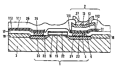
Fig. 1 is a cross-section of a i~.,.i, .-...l... l-" device according to the
invention. The ~ - l- ,. device comprises a ~ - body 3 with a
5 ~ element 1 in this case a transistor, having an electrically conducting region 5
on which a capacitor 2 forming a memory element is present with a lower electrode 11, an
oxidic f~ u.,l~,..LIi- dielectric 12, and an upper electrode 13, which lower electrode 11 makes
electrical contact with the conducting region 5 and comprises a layer 112 with a conductive
metal oxide and a layer 111 comprising platinum. The transistor 1 and the capacitor 2 are
10 ;A~ CUII~ by switching electrûnics. It is possible tû switch the r~,l-u~ dielectric 12
between two stable ~ i-," states by means of tbese switching electronics. For the sake
of clarity, only one transistor 1 and one capacitor 2 have been drawn, but in practice the
ù"~ body 3 will comprise very many such transistors and capacitors. The MOS
transistor depicted in Fig. 1 is provided in the silicon ,~ body 3 in a usual
15 manner, with a gate electrode 15 of pûlycrystalline silicon which is insulated from the
bûdy 3 by a silicon oxide layer 16 ûf a~ , 30 nm thickness. The
gate electrode 15 is furtber insulated by a layer of silicon oxide 17. Individual t}ansistors are
mutually separated by field oxide regiorls 18. Drain and source regions 20 and 21 of the
transistor are made between field oxide 18 and gate electrode 15 by means of diffusion. The
20 MOS transistor of Fig. 1 is ~llallur~ Lulcd in a known manner.
The aim is, for reasons of economy, to realise as many memory elements per unit surface
area as possible on a body 3. This means in practice that the memory
elements are often provided on conductive regions of ~ elements such as contact
pads, electrodes of switching transistors, and through .~ (vias, plugs). These
25 conductive regions comprise materials such as doped silicon, silicide, or metal. In the
example of Fig. 1, the conducting region 5 comprises a tungsten leâd-through region (plug).
Such tungsten plugs are widely used in practice. Since tungsten oxidi~es very readily, theR
will often be a too high contact resistance between the conducting region and the lower
electrode in known ~. -,;~ u~.l... l,-- devices.
According to the invention, the device is ,l-- ,-- ~ ;,- l in that the layer
111 comprising platinum contains more than 15 atom% of a metal capable of forming a
conductive metal oxide, and the layer 112 comprising the conductive metal oxide is present
between the layer comprising platinum and the f~,luC~ L~i~ dielectric 12. It is achieved
thereby that there is a good electrical contact between the lower electrode 11 and the
21780~1 ~
wo 96/1084~ - r~ ".
conducting region S after m~lm-f~-~h-re of the ~ device. Ruthenium is preferablychosen as the metal capable of forming a conductive metal oxide.
Figs. 2 and 3 show graphs of data recorded by Auger Electron
S~.C.,LIU~.U~UY (AES). A sputtering time t is plotted horizontally in these Figures. This
5 sputtering time is a measure for the depth below the surface of the lower electrode 11. An
atomic c~ in at% is vertically plotted in Figs. 2, 3. Fig. 2 shows how a tungsten
oxide layer is formed at the boundary 4 between the conducting tungsten layer 5 and the
layer 11 ~UIIIIUliDill~; platinum, given an atomic percentage oFA~Iul, 'y 10% ruthenium
in platinum after a heat treatment of 1 hour at 550 C m an N~IO~ dlulu~uh~ Fig. 3 shows
10 that only a very small quantity of oxygen is present at the boundary 4 for a ruthenium
percentage above 15%, in this case a~lJl, ly 30%, after a heat treatment of 1 hour at
600 C in an N~/O~ dilllU~UIl lc. It is suspected that this oxygen had already been present
before the lower electrode 11 was provided. This quantity of oxygen is i.. rr;.. 1 for
forming a closed tungsten oxide layer on the tungsten of the conducting region 5.
A first ~.. l,ù~ of a ! ' device is made as follows (see
Figs. 4, 5 and 1). Fig. 4 shows how first a switching transistor I with a gate electrode 15,
drain region 20, and source region 21 is provided in the ~.. :.. l.. l.~ body 3 in known
manner. The gate electrode 15 and the drain and source regions 20 and 21 are provided with
silicide layers 22 m known manner. The transistor is screened off witb a pllu~llulu~ silicate
20 glass layer 17 (PSG) which is ...A. r- S- cd in known manner. This layer 17 is provided ~
with tungsten plugs 25, 5 at the areas of the drain and source regions 20, 21, l-,~ .ly, in
known manner, so as to form the conductive region 5 above the source region 21. Then a
layer of 200 rlm platinumlruthenium (70130 atom%) is provided over the surface of the
~....;~.:,...l... l.,, body 3. This layer is sputtered at a pressure of 0.65 mPa argon at room
25 . c (RF spu~hering, 500 W power). Two sputtering sources are used here, whichdeposit alternately a ruthenium layer and a platinum layer of _~ / 1 to 1.5 nm
thickness. It is ad~ _ here when a platinum layer is provided as the final layer. The
layers provided are then baked fûr 1 hour at 600 C in an N~IO~ 80120 dLIllu~ lc. A lower
electrode 11 is created thereby with a structure according to the invention as shown in Fig.
30 3. A better surface of the lower electrode is obtained after baking in that the final layer
provided was a platinum layer. It is found that an oxidic f.llu.l~.LIi. dielectric 12 provided
on a lower electrode 11 having such a surface is highly resistant to defects in the dielectric
12 such as arise from known fatigue effects. The oxidic r~l~u~ LIi~ dielec~hric 12 is
lly prûYided ûn the lûwer electrûde 11. This rcl~u~ Lliu dielectric is a known
WO 96/1084S 2 1 7 8 ~ 9 1 ~ P~_IIIL,.,. ,.. --
substance, in tbe present example lead-~irconium titanate (PZT), which is pro~ided in known
marlner by a sol-gel technique. This starts with a solution of lead acetate, zirconium
butoxide, and titanium n-butoxide in ~ Lllu~ lul in a UUlyUDi~iUII of 1.1:0.35:û.65
(ayyll 1!/ 0.45 molar c.,... ~..11,.1;.~..), This solution is p}ovided on the lower electrode in
5 a centrifuge spinning process (rotation speed 2500 rpm, 30 s).. After the layer 12 has been
provided, it is baked for 30 minutes at 550 C rn an oxygen ,' c. The layer thickness
of the f~ u.l.,.,LIi~_ material obtair~ed in one spinning process and one baking cycle is
~yyl~ 0.1 ,ILm. To obtain a desired layer thickness of ~yy.~ 0.2 ~m, this
process is carried out twice. Then tne layer is baked for 1 hour at 600 C. A typical
10 C~ of the lead-zirconium titanate obtained by the above process is Pb~ oZrO 35Ti3 6503.
Altematively, a known technique such as sputtering or Ul~ ` chemical vapour
deposition (OMCVD) may be used. It is also possible to use lead titanate (PT), lead-
lanthanum-zirconium titanate (PLZT), or some other Icnown oxidic f~llU~ .,LIic dielectric. A
platinum upper electrode 13 is provided on the dielectric 12 tbrough sputtering (see Fig. 5).
15 The npper electrode 13, the dielectric 12, and the lower electrode 11 are pattemed by
rh-.tolill..,~;...l.~,;. ~1 and etching techniques. The layer 111 comprising platinum is not etched
away during this at the area of tbe tungsten plug 25 (see Fig. 1). The layer comprising
platinum 111 then fomms an electrical comnection between the drain region 20 and further
parts of the ~,...;. ,,...li.. ~... device. The layer platinum is thus used as an additional wiring
20 layer on the surface of the ~,.~-- .. li.. 1''l body 3. The surface of the s .. ;.. ",.l.. l.. , body 3
is then covered with an insulating PE (plasm~ L.~ d) CVD silicon oxide layer 26.Contact holes are etched into this layer, wherein a titanium/tungsten barrier layer and an
aluminium wiring layer 27 are provided in known manner. A ,~ device thus
,...,..ri" ~,.,C~l has a very low resistance between the conducting region S and the lower
25 electrode 11, i.e. in practice ~Iyy~ , 10-8 S)/cm~.
Fig. 6 shows a second ~ I ' of a ~- ; .,...l... l~,. device according
to the invention. Here a layer 110 of the metal capable of forming a conductive oxide is
present between the layer 111 comprising platinum and the conducting region 5. The
l,, "", l,;~ to oxygen of the layer 111 comprising platinum is strongly reduced also in this
3û ~ ...l,o~l;.,. .~ Such a device is Cu~y~l~Li~ly easy to l,l~l.ur~ u-c. Starting with an MOS
transistor covered with a LJIlClDyllOlUUD silicate glass layer 17 with a tungsten lead-through
region 5 as in the previous ~..,l,.-.l;..l. .1l (Fig. 4), a layer of lOû nm ruthenium with a layer
of 100 nm platinum thereon is provided on the conducting region 5. Said layers are sputtered
at a pressure of 0.65 mPa argon at room t~,llly~ ulc (RF sputtering, 50û W power). Then
217~0~ 1 WO96/1084S r~ '
the layers provided are baked for 1 hour at 600q C in an N2/02 80/20 aL l.o~ .c. This leads
to a lower electrode 11 which comprises m that order a ruthenium layer 110 with
~,, 'y 25 atom% platinum, a platinum layer 111 with ~ 'y 15-20 atom%
ruthenium, and the ruthenium oxide layer 112. It is suspected that both the
5 ruthenium/platinum 75/25 layer and the platinum/ruthenium 85/15 layer play a part in
blocking the oxygen diffusion. It is noted that AES analyses show that the surface of the
lower electrode 11 is enriched with platinum. It is suspected that this ~ h ", -1 Ieads to a
good structure of the oxidic ~I~u~l~..L~ ly provided on this surface. In a knownsputtering process, PZT is then provided on the lower electrode as the îcllu~l~.Lli~. dielectric
10 12, and platinum as the upper eleetrode 13. The upper electrode 13, the dieleetrie 12, and
the lower eleetrode 11 are then patterned in krlown manner by phrtrli~ .l ;r~l teehniques
and etehing. The ~ l deviee is fmished in known manner by the ~rFIirqtir~n of a
PE CVD silieon oxide layer 26 and the provision of eontaeting means 27 for the upper
eleetrode 13. This ~ ."l,o.l;",. : also has a very good eleetrieal eontaet between the
15 eondueting region 5 and the lower electrode 11, i.e. 10-8 S2/cm2.
The invention is not limited to the ~ .l,.~i;..-- ;~ described above. Thus,
fo} example, the .. I,o.l;.. l~ 1 and 2 may be combined. In that ease first a ruthenium layer
is provided on the eondueting surfaee 5, after whieh a platinum/ruthenium layer is provided
through u.i. l~r~ l;..., r~ u~c, the eapaeitor 2 is placed on a souree region of an MOS
20 transisto} 1 in the ~ ' It will be obvious that aloernative switching elements such
as, for example, bipolar transistors may also be used. r..l~;l.,ll"ul~, the condueting region 5
may eomprise materials other than tungsten, for example doped silicon, silicide, silicon-
~, or metals other than tungsten. Certain techniques for .. r~l 1.,. i.. , the,~.";~"" l l.~. device were mentioned above, but this implies by no means that the method
25 according to the invention can oniy be; ~ i by such ~Prhniri~ c Thus, for example,sputtering for the provision of the electrodes 11, 13 may be replaced by alternative
techniques such as chemical vapour deposition (CVD~ or Cl~LIu~ l deposition. Therc~u~ Lli~, dielectric may be provided by sputtering instead of by a sol-gel technique. Por
more details on known t~P~hn~ P~, the reader is referred to manuals such as S.M. Sze:
30 "VLSI Technology", Mc-Graw-Hill Book Company, and S. Wolf: "Silicon Processing for
the VLSI Era", vols. 1, 2, Lattice Press.