Note : Les descriptions sont présentées dans la langue officielle dans laquelle elles ont été soumises.
2179044
-1-
IC CARD WITH BOARD POSITIONING MEANS
BACKGROUND OF THE INVENTION
IC cards, which are often memory cards, are
commonly constructed with a molded plastic frame.
Front and rear connectors are mounted and/or molded
into the frame, and top and bottom covers are mounted
on the frame. U.S. Patents 5,207,586 and 5,244,397
show IC cards of this construction. U.S. Patent
5,242,310 shows a card of this construction, with the
front connector having frame parts and having brackets
with pintles received in notches of a circuit board.
U.S. Patent 4,924,076 shows a card in which a
connector has sideward projections received in slots
of a housing. If the number of parts to be
constructed and assembled were reduced, the IC cards
could be constructed at lower cost.
SUMMARY OF THE INVENTION
In accordance with one embodiment of the
present invention, a low cost IC card includes a
circuit board with its forward and rearward end
portions respectively mounted on forward and rearward
connectors, without requiring an intermediate frame.
The cover is also mounted on the front and rear
connectors and is connected to the circuit board
substantially only by an electrical ground connection.
At least a first connector has a laterally-
extending row of contacts that engage corresponding
contact pads on an end portion of the circuit board.
At least the first connector also has pegs lying
laterally beyond opposite ends of the row of contacts.
Each circuit board end portion has holes at its
opposite sides which receive corresponding pegs.
In accordance with the present invention,
there is provided a frameless IC card comprising a
circuit board assembly (30) having a circuit board
(32) with circuit components (31) thereon, said
t
2179044
-2-
circuit board having forward and rearward end portions
(34, 36) with said forward end portion having a row of
contact pads (42) thereon, said IC card including
front and rear connectors (12, 14) with at least said
front connector having a laterally extending row of
contacts (20) engaged with said contact pads, and said
IC card having a conductive sheet metal cover (60)
with upper and lower portions (66, 68) that lie
respectively above and below a majority of said
circuit board, characterized by: said connectors
having support surfaces (94, 150, 152, 206, 208, 210)
thereon, with said support surfaces of said front
connector being spaced from said contacts, and said
circuit board end portions are each rigidly mounted
directly on a corresponding one of said support
surfaces of one of said connectors; said sheet metal
cover is mounted directly on each of said connectors,
and said sheet metal cover is substantially free of
rigid connection to said circuit board independently
of said connectors; said front and rear connectors are
connected together substantially only by said circuit
board and said sheet metal covers.
In accordance with the present invention,
there is further provided an IC card which includes a
circuit board having front and rear board end
portions, front and rear connectors having about the
same width as said circuit board and each coupled to
one of said board end portions, and an electrically
conductive cover that has upper and lower portions
that lie respectively above and below a majority of
said circuit board, characterized by: said front
connector has support parts (95, 97) that include a
support surface and a plurality of pegs (90, 92, 90A)
that each have lower ends anchored at one of said
support parts and upper ends that project up above the
support surface, with said support parts forming
21 79~ 44~
-3-
board-supporting surfaces (94, 150, 152); said circuit
board front end portion has drilled round holes (100,
102, 162, 164, 172, 174) that are spaced from the
board edges and that receive corresponding ones of
said pegs, with said circuit board end portions having
mount parts (85, 87) lying adjacent to said pegs and
supported on said board-support surfaces.
In accordance with the present invention,
there is further provided an IC card which includes a
circuit board (32) having front and rear board end
portions (34, 36), at least a front connector (12)
coupled to said front board end portion and an
electrically conductive cover (60) that has upper and
lower portions that lie respectively above and below a
majority of said circuit board, characterized by:
said front connector has support parts (95, 97) that
include a plurality of pegs (90, 92, 90A, 192) that
each have lower ends anchored at one of said support
parts and upwardly projecting upper portions, with
each of said peg upper portions having a plurality of
vertically stacked peg parts (140, 142, 144, 200, 202,
204) and at least one supporting surface (150, 152,
208, 210) lying above said connector support surface;
said circuit board front end portion has holes (100,
102, 162, 164, 172, 174, 212, 216, 218) that receive
corresponding ones of said pegs, with said circuit
board end portions having mount parts (85, 87) lying
adjacent to said pegs and supported on said supporting
surfaces.
In accordance with the present invention,
there is further provided a front connector for use in
an IC card which includes a circuit board (32) having
front and rear board end portions (34, 36),
characterized by: said front connector has support
parts (95, 97) that each includes a lower board
support surface and at least one peg (90, 92, 90A,
21 79044
-3a-
192) with a lower end anchored to the support part and
an upwardly projecting portion, with each of said peg
upwardly projecting portions having a plurality of
vertically stacked peg parts (140, 142, 144, 200, 202,
204) and at least one board supporting surface (150,
152, 208, 210) lying above said connector support
surface .
In accordance with the present invention,
there is further provided a method for constructing an
IC card, which includes forming front and rear
connectors (12, 14) with laterally opposite sides and
with at least said front connector having a laterally
extending row of contacts (20), forming a circuit
board (32) with front and rear board end portions (34,
36) each having laterally-spaced opposite sides and
with a laterally extending row of contact pads (42) on
at least its front end portion, forming an
electrically conductive cover (60), and assembling
said connectors, circuit board, and cover into an IC
card, characterized by: establishing at least one
upstanding peg (90, 92, 90A) at each laterally
opposite side of each connector, with the pegs on said
front connector lying on laterally opposite sides of
its row of contacts; said step of forming said circuit
board includes drilling round holes (100, 102, 162,
164, 172, 174) in said front and rear board end
portions with said holes in said circuit board front
portion spaced from the board edges and lying
laterally beyond said rows of contact pads, and
including placing said circuit board end portions so
said pegs are received in said holes.
In accordance with the present invention,
there is further provided a frameless IC card which
includes a housing for holding a circuit board
assembly (30) that includes a circuit board (32) and
components (31) on the circuit board wherein the
2~~9044'
-3b-
circuit board has front and rear board end portions
(34, 36) that each have holes (100, 102, 162, 164,
172, 174, 212, 216, 218), with at least said front
board end portion having a row of conductive pads
(42), front and rear connectors (12, 14) with at least
said front connector having a row of contacts (20) for
engaging said row of conductive pads, with each of
said connectors having a support part (91, 95, 97)
that forms a support surface (94, 150, 152, 206, 208,
l0 210) adapted to support said front and rear board end
portions, respectively, of said circuit board and with
the support surfaces of said front connector being
spaced from said row of contacts, and a cover (60) for
substantially enclosing said circuit board with said
cover having forward and rearward cover end portions
(75, 73) and with each of said cover end portions
having parts (110, 112, 115, 116) for attachment to a
corresponding one of said connectors, characterized
by: a plurality of pegs (90, 92, 90A, 192) that each
have lower ends anchored to one of said connectors at
a support surface thereof and that each have upper
ends received in one of said circuit board holes; each
of said pegs has a plurality of vertically stacked peg
parts (140, 142, 144, 200, 202, 204) and has at least
one board supporting surface (150, 152, 208, 210)
lying above said connector support surface.
In accordance with the present invention,
there is further provided an IC card comprising a
circuit board assembly (30) having a circuit board
(32) with circuit components (31) thereon, said
circuit board having forward and rearward end portions
(34, 36) with said forward end portion having a row of
contact pads (42) thereon, said IC card including
front and rear connectors (12, 14) with at least said
front connector having contacts (20) engaged with said
contact pads, and said IC card having a conductive
2~ 790 ~4~
-3c-
sheet metal cover (60) with upper and lower portions
(66, 68) that lie respectively above and below a
majority of said circuit board, characterized by:
said sheet metal cover comprising lower and upper
cover halves (66, 68) having coincidental vertical
axes, said lower cover half comprising a lower sheet
(64) having opposite sides and a pair of lower flanges
(74, 76) extending upwardly at said sides, and said
upper cover half comprising an upper sheet (62) having
opposite sides and a pair of upper flanges (70, 72)
extending downwardly at said sides thereof and lying
outward of and substantially against said lower
flanges, with said upper flanges having lower ends
bent inwardly to lie under said lower cover sides;
said upper sheet has a lower surface, and said lower
flanges have upper ends that each substantially abuts
said lower surface of said upper sheet.
The novel features of the invention are set
forth with particularity in the appended claims. The
invention will be best understood from the following
description when read in conjunction with the
accompanying drawings.
BRIEF DESCRIPTION OF THE DRAWINGS
FIG. 1 is an isometric view of an IC card of
the present invention, and showing, in phantom lines,
a portion of an electronic device that receives the
card.
FIG. 2 is an exploded isometric view of the
IC card of FIG. 1.
FIG. 3 is a partial exploded view of a
connector and of a circuit board end portion that can
mount thereon.
FIG. 4 is a partial sectional view taken on
line 4 - 4 of FIG. 3, showing the parts in an
assembled position.
FIG. 5 is a partial sectional view of the
21 79~ 44
-3d-
connector and circuit board of FIG. 4, and also
showing two other circuit boards which can be used.
FIG. 6 is a partial sectional view of the IC
card of FIG. 1.
FIG. 7 is a partial sectional view of the IC
card of FIG. 1.
FIG. 8 is a partial isometric view of a peg
constructed in accordance with another embodiment of
the invention.
FIG. 9 is a partial exploded view of a peg
and circuit board constructed in accordance with
another embodiment of the invention.
DESCRIPTION OF THE PREFERRED EMBODIMENTS
FIG. 1 illustrates an IC card 10 which has
connectors 12, 14 at its opposite ends. The
connectors 12, 14 can be designated respectively as
front and rear connectors, although the opposite could
be done. The card is designed to be inserted in a
forward direction F into an electronic device 16,
until contacts 20 on the front connector engage
corresponding contacts 22 of the electronic device.
The card is withdrawn in a rearward direction R. IC
cards have standard maximum dimensions under PCMCIA
(PERSONAT~ COMPUTER MEMORY CARD INTERNATIONAL
ASSOCIATION) standards, of 5mm in upward and downward
directions U, D, of 54mm in lateral directions L, and
of 85.6mm in longitudinal directions F, R. The IC
card should be constructed at low cost while providing
maximum utilization of the limited space within the
card to hold electronic components.
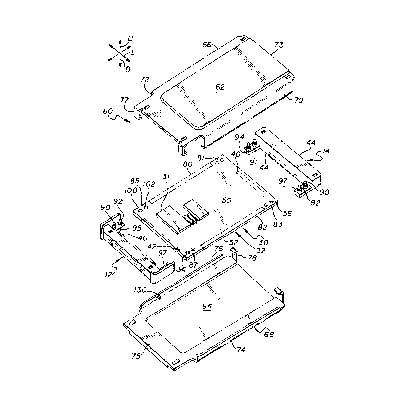
FIG. 2 shows that the IC card includes a
circuit board assembly 30 with electronic components
31 such as integrated circuits, resistors, capacitors,
etc., which are mounted on a circuit board 32. The
circuit board has laterally opposite side 80, 82 and
forward and rearward end portions 34, 36, and has
21 790 ~4~
-3e-
laterally-extending rows of contact pads 40, 42 at its
opposite end portions. The front and rear connectors
12, 14 each include a block of molded plastic. At
least the front connector 12, and preferably both
connectors, have at least one laterally extending row
of contacts with contact tails 44, 46 constructed to
engage corresponding rows of contact pads 40, 42 on
the circuit board. It is noted that the circuit board
has upper and lower surfaces 50, 52, and the contact
l0 pads are normally located on the lower surface 52.
A cover 60 is designed to surround the
circuit board assembly. The cover includes upper and
lower cover parts 66, 68 that have sheet-like portions
62, 64 that lie respectively above and below a
majority of the surface area of the circuit board.
The upper cover part includes a pair of upper side
flanges 70, 72, which engage corresponding lower side
flanges 74, 76 on the lower cover part. The parts are
assembled by first mounting the circuit board opposite
end portions on the connector 12, 14. This
subassembly is placed in the lower cover part 68. The
rear 73 of the upper cover part is placed at the front
75 of the lower one, and the upper cover part is slid
in the rearward direction R. U-shaped fingers 77, 78
at the front and rear of corresponding cover parts
help to keep the fully assembled cover parts in place
on the connectors.
Previous PCMCIA IC cards have used a molded
plastic frame which held the other parts together.
U.S. Patents 5,207,586 and 5,244,397 show IC cards of
this type, wherein the molded plastic frame extended
between the front
WO 95/16976 21 l 9 0 4 4 pCT/US94112683
-4-
and rear connectors and held them rigidly in place, supported the circuit
board
assembly, and supported top and bottom cover parts. Although in previous
and present IC cards there is some mechanical connection between the circuit
board and the connectors through the soldering connection of the rows of
contact tails or contacts 44, 46 with the conductive pads 40, 42 on the
circuit
board, such solder connections cannot be relied upon for strong mechanical
coupling, which was previously achieved by the molded plastic frame.
In accordance with the present invention, applicant provides a
frameless IC card wherein the opposite end portions 34, 36 of the circuit
board,
mount directly on the front and rear connectors 12, 14. The rear end portion
36 of the board has board mount parts 81, 83 at its opposite sides, that mount
on the rear connector 14, and the front end portion 34 of the board has board
mount parts 85, 87 that mount on the front connector 12. The connectors have
corresponding support parts 91, 93, 95 and 97, with all mount parts being
similar and all support parts being similar. Each connector, including its
support parts, has a longitudinal length (in directions F, R) that is less
than
one-half the longitudinal length of the card, and preferably that is less than
one-
'fourth as much. As shown in FIG. 3, each circuit board mount part such as 81,
extends laterally beyond a corresponding row of contact pads 42 (e.g.
laterally
beyond an end of the row). Each board mount part such as 81 of the circuit
board end portion is directly mounted on a corresponding connector support
part such as 91 which extends laterally beyond a corresponding row of
contacts 46. Each support part such as 91, includes first and second
platforms, or projections, or pegs 90, 92 that extend up from a first board-
supporting surface 94. The side 80 of the circuit board which forms the mount
part 81, has a pair of holes 100, 102 that are designed to closely receive the
corresponding pegs 90, 92. Thus, the front and rear connectors form an
Wp 95!16976 217 9 0 4 4 pCT~S94/12683
-5-
apparatus for holding the circuit board. Each of the pegs preferably has
several steps, which will be discussed below.
With the front and rear portions of the circuit board securely
mounted on the front and rear connectors, the cover can be placed around the
circuit board and connectors. FIG. 6 shows the manner in which the upper
and lower cover parts 66, 68 are mounted on the front and rear connectors 12,
14. The upper cover part 66 has downwardly-inclined tabs 110, 112 which
project into corresponding recesses 114 at the tops of the connectors. The
lower cover part has tabs 115, 116 that project into corresponding recesses
117 at the bottoms of the connectors. The tabs form connect parts that mount
the cover ends to the connectors, to thereby attach the cover parts to the
connectors. Cover parts such as 118 lying against the connectors also form
connect parts. Adhesive also can be used to hold the cover parts to the
connectors. The cover parts also have interfitting side flange parts (FIG. 7).
It is noted that the covers are directly mounted on the front and rear
connectors, as is the circuit board 3C~. No intermediate frame apart from the
cover parts and circuit board, extends between the connectors. It is noted
that
there is a grounding electrical connection between the cover and a ground
plane of the circuit board. FIG. 7 shows that the lower cover part 68 has-a
tab
130 which engages a location on a ground plane 132. However, this does not
provide a rigid connection or mechanical support, and there is substantially
no
other direct connection between the circuit board and cover.
FIGS. 3 and 4 show that each platform or peg 90, 92 has a
plurality of peg parts or steps 140, 142, and 144. The first step 140 is of
greatest width A, while the second and third steps 142, 144 have progressively
smaller widths B and C. The support part 91 forms board-supporting surfaces
or surface regions 94, 150, 152 at the bottom of each step. The holes such as
100 in the circuit board 30, are shown in FIG. 4 as having a hole width B so
the
WO 95/16976 217 9 0 4 4 pCT/US94/12683
-6-
walls of the circuit board holes are closely received in the second steps 42,
and
the lower surface of the circuit board rests on the second board-supporting
surface region 150.
The connectors 12, 14 (FIG. 2) and cover 60 are usually made by
a manufacturer who makes large volumes of such connectors and covers. The
connector and cover manufacturer commonly sells such parts to a firm that
designs and constructs a circuit board with its own circuitry thereon, and
assembles the circuit board to the connectors and cover to form a complete
IC card. The circuit board manufacturer usually has drills that can form the
holes such as 100, 102 so the holes are of a closely controlled width or
diameter, and in a pattern wherein the holes are precisely located. The
circuit
board manufacturer can choose the particular height of the circuit board by
choosing the diameter of the circuit board holes that he drills. A particular
height of the circuit board above the first surface 94, is chosen so that the
desired circuit components can be mounted on the circuit board. If an
engineer vvho designs the circuit board requires components of large vertical
thickness, he may drill small holes so that the circuit board rests on the
third
platform 152 (FIG. 4). This will leave a relatively thick space below the
bottom
of the circuit board, on which the thick component can be mounted. However,
it will leave little room for mounting components on the upper surface of the
circuit board. On the other hand, if the engineer wishes to cram a large
number of circuit components of moderately small thickness onto the board,
he can use large diameter holes so the circuit board rests on the first
surface
94. This will leave thick spaces both above and below the circuit board,
between the board and the covers 66, 68.
FIG. 5 shows another circuit board 160, that is similar to the circuit
board 30, but wherein the circuit board 160 has holes 162, 164 to enable it to
be received by the lowermost step or peg part 140. The figure also shows still
Wp 95116976 217 9 0 4 4 pCTNS94/12683
_7_
another circuit board 170 with smaller holes 172, 174 that enable it to be
closely received by the third pegs or steps 144.
A variety of approaches can be used to securely fasten the circuit
board in place after its holes have received the pegs. One method is to use
simple press fitting. Another method is to use adhesive which will adhere the
lower surface and the walls of its holes to the peg and/or the lowermost
surface
94. FIG. 8 shows a modified peg 90A with a slot 150 that permits the peg to
be compressed when a circuit board is pressed firmly in place. In FIG. 8, the
peg 90A is manufactured separately from the connector 12A, with the peg
having a post 152 press fitted into a hole in the connector.
FIG. 9 illustrates part of an assembly 180 of another embodiment
of the invention, wherein each peg or platform is of rectangular shape as seen
in a plan view taken along vertical line 194. A particular peg or platform 192
has three steps 200, 202, 204 and three corresponding board-supporting
surfaces 206, 208, and 210. The circuit board 211 has a hole 212 designed to
receive one of the steps, with the particular hole 212 shown in solid lines
being
designed to receive the uppermost step 204, so the lower surface 214 of the
circuit board lies on the board-supporting surface 210. FIG. 9 shows two other
hole sizes 216, 218 of different widths to enable the circuit board to lie at
progressively lower heights. The holes such as 212 are in the form of slots
that
extend to the extreme side edge 220 of the circuit board. While such slots are
not as easy to form as round holes, they can be formed by saws that cut into
the edge of the circuit board. FIG. 9 also shows that the circuit board 211
has
a ridge or integral beam portion 222 that increases the longitudinal rigidness
of the circuit board.
Although terms such as "vertical", "horizontal", "upper and lower",
etc, have been used herein to describe the parts of the IC card as shown in
the
WO 95/16976 217 9 0 4 4 PCT/US94/12683
_g_
figures, it should be understood that the IC card and its parts can be
assembled and used in any orientation with respect to gravity.
In the arrangements illustrated, each end portion of the circuit
board is rigidly connected to a corresponding connector at locations laterally
beyond the row of connector contacts. It is possible for the circuit board to
extend rearwardly and forwardly slightly further and to mount to connector
locations that lie above the row of contacts. However, such mounting is more
difficult because it requires the portions of the connector that hold the
front
contact portions to be thinner. In the case of the front connector which
typically has two vertically spaced rows of contacts (but with the tails
usually
lying in one row), there is very little room for such mounting. By mounting
the
circuit board on laterally opposite sides of each connector, applicant uses
connector portions that may not be otherwise utilized and which can be easily
made to be thinner than the contact-holding portions. In some cards, no
contacts are required at the rear of the card, in which case the rear
connector
can be formed by a block of molded plastic without contacts, and the rear
connector serves primarily to mechanically connect the rear end portion of the
circuit board to the cover parts and to close the rear of the space between
the
cover parts.
Thus, the invention provides an IC card which is of simplified
construction. The IC card is frameless, in that opposite end portions of the
circuit board are directly and rigidly connected to front and rear connectors.
The cover can include upper and lower cover parts or a one-piece cover, that
are also directly mounted on the connectors. All of this is preferably
accomplished without the use of a separate frame that would extend between
the front and rear connectors and which would support the circuit board and
cover parts. The connection of each circuit board end portion to a connector
is preferably accomplished at locations laterally beyond the row or rows of
WO 95/16976 217 9 0 4 4 PCT/US94/12683
_g_
contacts of the connector, at least at the front connector, so that attachment
occurs in connector regions of moderately small vertical thickness. Such
connections can be accomplished by providing upstanding pegs on the
connectors, which are received in holes formed in the circuit board. The pegs
are preferably of circular shape as seen in a plan view, so that they can be
received in round holes that can be simply drilled by circuit board makers.
The
pegs can have at least two different steps, with a board-supporting surface at
the bottom of each step, and with the higher step or steps having smaller
widths than the lower one. This enables a circuit board maker to choose which
step will be received, by choosing the width or diameter of the hole that he
will
form in the circuit board.
Although particular embodiments of the invention have been
described and illustrated herein, it is recognized that modifications and
variations may readily occur to those skilled in the art, and consequently, it
is
intended that the claims be interpreted to cover such modifications and
equivalents.