Note : Les descriptions sont présentées dans la langue officielle dans laquelle elles ont été soumises.
79~6b
OUTPUT STAGE OF OPERATIONAL AMPLIFIER SUITABLE FOR
MOUNTING ON A SUBSTRATE AND METHOD OF AMPLIFYING
THEREWITH
l O
Background of the Invention
1. Field of the Invention
The present invention relates generally to amplifiers and more
specifically to output stages of operational amplifiers.
2. Description of the Related Art
Generally, an operational amplifier (op amp) is used in many
applications which include, but are not limited to, radiotelephones. In
fact, current radiotelephones include multiple op amps for increasing
signal power in both the receiver and the ~ldl~ . Such op amps
2 5 are typically mounted, along with other circuitry, on a substrate of an
ldLed circuit (IC). As radiotelephones become smaller and more
portable, there is a growing need for the op amps to operate effectively
at low power supply voltages.
Op amps consist of an input stage, an irlt~rmPr7i~t.~ stage, and an
3 0 output stage. When the op amp is mounted on an IC at a signal output
thereof, it is necessary for the output stage of the op amp to provide a
low impedance output. The low impedance output prevents the
remairlder of the circuit mounted on the IC from becoming unstable
from large amounts of capacitance provided by other directiy coupled ~ ~-
-
21 ~9~5
-2-
ICs or other components. Unfortunately, many of the existing op amp
output stages, including those with the capability of swinging rail-to-
rail, exhibit a high output impedance.
FIG. 1 is an illllctr;3ti~n in schematic form of a known low
5 impedance output stage for an op amp comprising an emitter (or
source) follower buffer 100. The buffer 100 is powered by a first supply
voltage rail (+VBB~ 102 and a second supply voltage rail 104. The buffer
100 includes an input 106 for receiving an input voltage 105. The input
106 is coupled to first and second buffering devices 108,110 via
respective first and second biasing devices 112,114. In response to the
input voltage 105, the first and second buffering devices 108,110
provide an output voltage 115 and an output current 117, collectively
an output signal, at an output 116 coupled thereto. The output signal is
capable of driving a load, such as another IC, (not shown) that is
coupled to the output 116 and similarly powered by the first and second
supply voltage rails 102,104.
FIG. 2 is an illustration in graph forrn of a known voltage
transfer characteristic 200 of the buffer 100 of FIG. 1. In response to the
input voltage 105, the first and second buffering devices 108,110
2 0 alternate operation to provide the output signal. As the input voltage
105 exceeds +VBB/2, as designated by portion 202 of the transfer
characteristic 200, the output current 117 is primarily sourced to the
output 116 of FIG. 1 by the first buffering device 108. As the input
voltage 105 falls below +VBB/2, as d~ci~n~tf~r~ by portion 204 of the
2 S transfer characteristic 200, the output current 117 is primarily sunk
from to the output 116 by the second buffering device 110. The first and
second biasing devices 112,114 ensure that the first and second
buffering devices 108,110, respectively, remain on to prevent crossover
distortion as the input voltage 105 a~ ale~ly equals, or passes
3 0 through, +VBB/2, as ~cign~t~d by point 206 on the transfer
characteristic 200.
Due to base-emitter junction electrical limitations of the bipolar
junction= transistors comprising the first and second biasing devices 108,
110, the buffer 100 is unable to provide the output signal arld drive the - ~
794~
-3-
load over a maximum voltage range 208. The maximum voltage range
208 is defined by the difference between the first and second supply
voltage rails 102, 104 and iPci~n~tpri as OV to +VBB. In fact, the buffer
100 is unable to provide the output signal when the input voltage 105
5 is within a diode drop of either the first or second supply voltage rail
102,104. A diode drop is commonly known as the voltage drop
between the base and the emitter of a bipo~ar junction transistor.
Therefore, the buffer 100 is effectively limited to operation in a buffer
voltage range 210 defined by the difference in the first supply voltage
l 0 rail 102 less a diode drop and the second supply voltage rail 104 less
another diode drop. Assuming that the diode drop is approximately
0.8V, the buffer voltage range 210 extends from approximately 0.8V to
approximately +VBB O.8V as depicted in FIG. 2.
In low power applications, the loss of operating range, or lack of
l 5 ability to swing rail-to-rail, due to the two diode drops creates a
substantial limit:~tion For example, if the first supply voltage rail 102
is 3V and the second supply voltage rail 104 is OV as shown, the
maximum voltage range 208 becomes 3V and the buffer voltage range
210 becomes d~LO~illiaL~Iy 1.4V. In such a scenario, the buffer 100
2 0 would be incapable of providing the output signal and driving the load
for more than half (d~,u;~i-l,ately 1.6V) of the 3V maximum voltage
range 208.
Therefore, what is needed is an output stage for an op amp
having rail-to-rail swing capability so as to be suitable for use in a low
2 S voltage application and having a low output impedance so as to be
suitable for mounting at the output of an IC.
Brief Description of the Drawings
FIG. 1 is an i~ tr:~ti~n in schematic form of a known output
stage of an operational amplifier;
FIG. 2 is an illustration in graph form of a known voltage
transfer characteristic of the output stage of FIG. 1;
2~79465
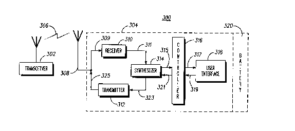
FIG. 3 is an illustration in block diagram form of a radio
frequency ( I-mmllnieiltions system employing~a radiotelephone;
FIG. 4 is an illustration in block diagram form, with limited
detail, of a synthesizer of the radiotelephone of FIG. 3, the synthesizer
5 employing an operational amplifier;
FIG. 5 is an illustration in schematic form of an output stage of
the operational amplifier of FIG.~4;
FIG. 6 is an illustration in graph form of a voltage transfer
characteristic of the output stage of F ti. 5; ~
l O FIG. 7 is an illustration in schematic form of an alternate output
stage of the operational amplifier of FIG. 4; and
FIG. 8 is an illustration in flow chart form of a method of
amplifying an input voltage.
l S
Detailed Description of the Preferred Embodiments
~ n output stage for an operational amplifier powered by a first
supply voltage rail and a second supply voltage rail includes a buffer
2 0 and a current booster for amplifying an input voltage into a low
impedance output signal. The buffer amplifies the input voltage into
the amplified output signal when the input voltage is within a buffer
voltage range, the buffer voltage range contained within a Illd~dlllUIII
voltage range defined by a voltage difference between the first supply
2 5 voltage rail and the second supply voltage rail. The current booster
assists the buffer in amplifying the input voltage into the amplified
output signal when the input voltage is outside of the buffer voltage
range but within the maximum voltage range.
FIG. 3 is an illustration in block diagram form of a radio
3 0 frequency .. ,""I",,.i~ mc system 300 wherein a L.dl.s.~iv~l 302 and a
radiotelephone 304 rrlnnmllnie:3t~ via radio frequency (RF) signals 306.
The L~ s.~iv~ 302 is a fixed site L-dns.t:iv~- serving a radio coverage
area populated by radiotelephones, such as radiotelephone 304. The
radiotelephone 304 includes an antenna 308, a receiver 310, a ~ ~~
-
1794S5
--5-
~la~ iLLL-~ 312, a ~y~Ll~esi~L-I 314, a controller 316, and a user interface
318. The radiotelephone 304 operates via power provided by a
detachable battery 320. The Lldns~;v~l 302 transmits RF signals 306
into its radio coverage area populated by the radiotelephone 304. The
antenna 308 transduces the RF signals 306 into electrical RF receive
signals 309 and couples the electrical RF receive signals 309 to the
receiver 310. The receiver 310 mixes the electrical RF receive signals
309 with a local oscillator frequency to generate int.ormP~ t.o frequency
(IF) receive signals 311. The receiver 310 couples the IF receive signals
311 to the ~yllLl~ l 314. The synthesizer 314 provides additional
mixing frequencies for converting the IF receive signals 311 into
baseband (BB) receive signals 315. The synthesizer 314 adjusts and
maintains the BB receive signals 315 at a desired amplitude for use by
the controller 316. The controller 316 processes BB receive signals 315
into data receive signals 317. The data receive signals are coupled to
the user interface 318 and output to the user as audible speech via a
speaker (not shown) and as operational inform:~hon via a visual
display device (not shown).
Speech input by the user via a microphone (not shown) of the
2 0 user interface 318 is transduced and coupled to the controller 316 as
data transmit signals 319. The controller 316 converts the data transmit
signals 319 into BB transmit signals 321. The BB transmit signals 321
are coupled to the synthesizer 314. The ~yl~ e~ l converts the BB
transmit signals 321 into IF transmit signals 323. The IF transmit
2 5 signals 323 are coupled to the tr~ncmit~r 312, which mixes the IF
transmit signals 323 with a local oscillator frequency to convert the IF
transmit signals 323 into electrical RF transmit signals 325. The
electrical RF transmit signals 325 are further transduced by the antenna
308 and transmitted to the ~Idlls.L-ivL~l 302 as RF signals 306.
3 0 FIG. 4 is an illustration in block diagram form of the
314 of the radiotelephone 304. The ~y~ i C:l 314 includes a
downconverter 401, a voltage controlled oscillator (VCO) 402, an op
amp 4Q3, and an upconverter 404. The IF receive signals 311 generated ~
by the receiver 310 of FIG. 3 are coupled to the do~lL~ vL lLL~l 401. The ~ . ~
~7~9465
--6 -
downconverter 401 performs quadrature demodulation on the IF
receive signals 311 by mixing the IF receive signals 311 with inphase
and uludLl~Lul~ components of a BB frequency signal 406 input to the
downconverter 401 from the VCO 402. The resulting inphase and
S quadrature receive signals are filtered by the downconverter 401 and
coupled to the op amp 403 as inh~rmf~ tf~ BB receive signals 408. The
op amp 403 adjusts the illlrl ~ l1;Ah, BB receive signals 408 to a desired
amplitude and outputs the ;Illr~ 1; lr BB receive signals 408 to the
controller 316 of FIG. 3 as BB receive signals 315. The op amp 403
I O includes an input stage 414, an il l lr~ r stage 416, and an output
stage 418.
The BB transmit signals 321 generated by the controller 316 of
FIG. 3 are coupled to the U~.UlIV~lL~l 404. The upconverter 404 mixes
the transmit BB signals with inphase and quadrature components of an
IF frequency signal 420 generated by the VCO 402. The mixed inphase
and quadrature IF signals are combined and output from the
UlU-UllV~ L 404 as IF transmit signals 323. The IF transmit signals 323
are further coupled to the 11~1L~ iLL~:1 312 of FIG. 3.
In the preferred embodiment, the components of the ~yllL~
2 0 314 shown in FIG. 4 are integrated and bonded to a suitable substrate
430, such as a ceramic substrate. The substrate 430 is mounted into an
IC package (not shown). The IC package provides pinouts for
connecting ~Ulll~U~ lIL~ of the ~yl~ e~ l 314, such as the output stage
418 of the op amp 403, to external LUlll~UUlltllL~, such as the controller
2 5 316 of FIG. 3 which may consist of one or more IC packages. When
coupling the BB receive signal 315 from an output of the IC package of
the ~yl~Ll~ l 314 directly to an input of the IC package of the
controller 316, the BB receive signal 315 encounters a large amount of
capacitance from the input of the IC package of the controller 316. In
3 O order to prevent the ~y~Ll~esi~l 314 from becoming unstable from this
high capacitance, it is necessary for the output stage 418 to provide a
low imre~1~n~f~ output.
FIG. 5 is an illustration in schematic form of the output stage 418 ~.
of the ol amp 403 of FIG. 4. In the preferred t:llll,U.lill~llL, the output ~ '~
~ ` 2~ ~46~
stage 418 is unity gain and includes the buffer 100 of FIG. 1 and the
current booster 500. The buffer 100, which is a push-pull circuit, is
powered by the first and second supply voltage rails 102,104 of the
battery 320 of FIG. 3. Although the second supply voltage rail 104 is
S shown as ground, it will be l~o~ l that the output stage 418 could
be powered via a split supply having positive and negative supply
voltage rails wherein the first supply voltage rail 102 remains +VBB
and the second supply voltage rail 104 is de~ign~tf~fl, for example, VBB.
The buffer 100 is coupled between the input 106 and the output
116 of the output stage 418 and includes the first and second buffering
devices 108,110 and the first and second biasing devices 112,114
generally described with respect to FIG. 1. More specifically, the first
buffering device 108 includes npn transistor 501 having a base, a
collector coupled to the first supply voltage rail 102, and an emitter
coupled to the output 116. The first buffering device 108 is biased to a
diode drop above the input voltage 105 by the first biasing device 11æ
The first biasing device 112 includes pnp transistor 502 having a base
coupled to the input 106, a collector coupled to the second supply
voltage rail 104, and an emitter coupled to the base of npn transistor
2 0 501 of the first buffering device 108, a first current source 503, and the
first supply voltage rail 102. In the preferred embodiment, the first
current source 503 could be implemented by a PMOS transistor.
The second buffering device 110 includes pnp transistor 504
having a base, a collector coupled to the second supply voltage rail 104,
2 5 and an emitter coupled to both the output 116 and the emitter of npn
transistor 501 of the first buffering device 108. The second buffering
device 110 is biased to a diode drop below the input voltage 105 by the
second biasing device 114. The second biasing device 114 includes npn
transistor 505 having a base coupled to the input 106, a collector
3 0 coupled to the first supply voltage rail 102, and an emitter coupled to
the base of pnp transistor 504 of the second buffering device 110, a
second current source 506, and the second supply voltage rail 104. In
the preferred embodiment, the second current source 506 could be
impler~iented by a NMOS transistor.
- 21~4~
The buffer 100 operates in response to the input voltage 105
applied at the input 106 as previously described with respect to FlGs. I
and 2. The first and second buffering devices 108,110 alternate
operation based on a magnitude of the input voltage 105 to provide the
5 output signal capable of driving a load, such as the controller 316 of
FIG. 3. However, as previously stated, the buffer 100, which realizes
base-emitter junction voltage limitAIinn~, is incapable of approximately
swinging rail-to-rail and providing the output signal when the input
voltage 105 is outside of the buffer voltage range 210 of FIG. 2 (when
the input voltage 105 comes within approximately 0.8V of either the
first supply voltage rail 102 or the second supply voltage rail 104). In
order to increase rail-to-rail swing capability so that the output signal
can be generated when the input voltage 105 is outside of the buffer
voltage range 210 of FIG. 2, the current booster 500 is coupled to the
buffer 100.
The current booster 500, which is powered by the first and second
supply voltage rails 102,104 and coupled between the input 106 and the
output 116 of the output stage 418, assists the buffer 100 in providing an
output voltage 520 and the output current 117, collectively the output
2 0 signal, at the output 116 when the input voltage 105 is outside of the
buffer voltage range 210 of FIG. 2. The current booster 500 permits the
output stage 418 to operate over a~plu,..ll.a~ly the maximum voltage
range 208 of FIG. 2 and still provide low impedance at the output 116.
The current booster 500, which is a rail-to rail swing circuit,
2 5 includes a first booster device 508 and a second booster device 510. The
first booster device 508 includes NMOS transistor 507 having a gate
coupled to the input 106, a source coupled to the second supply voltage
rail 104, and a drain coupled to the output 116. The first booster device
508 further includes a first current mirror 512. In the preferred
3 0 embodiment, the first current mi}ror 512 comprises PMOS transistors
511 and 513. The first current mirror 512 is coupled between the drain
of NMOS transistor 507 of the first booster device 508 and the output
116. Th=e second booster device 510 includes PMOS transistor 509
having a gate coupled to the input 106, a source coupled to the first ~ .
~ ~ 21 7~465
g
supply voltage rail 102, and a drain coupled to the output 116. The
second booster device 510 further includes a second current mirror 514.
In the preferred embodiment, the second current mirror 514 comprises
NMOS trAncic~orc 517 and 518. The second current mirror 51~ is
coupled between the drain of PMOS transistor 509 of the second booster
device 510 and the output 116.
The current booster 500 operates as follows. As the input voltage
105 approaches the first supply voltage rail 102, the first booster device
508 turns on and causes a first booster current 515 to flow into the drain
l 0 of NMOS transistor 507 of the first booster device 508. The first booster
current 515 is mirrored or inverted by the first current mirror 512 and
coupled to the output 116. As the input voltage approaches the second
supply voltage rail 104, the second booster device 510 turns on and
causes a second booster current 516 to flow out of the drain of PMOS
15 transistor 509 of the second booster device 510. The second booster
current 516 is mirrored or inverted by the second current mirror 514
and coupled to the output 116.
FIG. 6 is an illustration in graph form of a voltage transfer
.I.~..I.I~li~tiC 600 of the output stage 418 of FIGs. 4 and 5. In response to
2 0 the input voltage 105, the first and second buffering devices 108,110
and the first and second booster devices 508, 510 alternate operation to
provide the output voltage 520 and the output current 117. As the
input vo~tage exceeds +VBB/2 and approaches +VBB, as llPci~n~Pd by
portion 602 of the transfer ~ h;~r;~iPric~ 600, the output voltage 520 is
2 5 generallyprovided by the first and second buffering devices 108,110
and the first booster device 508. Specifically, the first buffering device
108 primarily provides the output voltage 520 and the output current
117 for values of the input voltage 105 between point 601 on the
transfer characteristic 600 (or approximately +VBB/2) and point 603 (or
3 0 approximately +VBB-0.8V). Between point 603 and point 605 (or
d~ aL~IY +VBB O.2V~, the output voltage 520 is provided by the
second buffering device 110 and the output current 117 is provided by
the firstbooster device 508. ,
--` . 21 7946~
-10-
For input voltages below +VBB/2 and approaching 0V, as
~IPcign~t~rl by portion 604 of the transfer characteristic 600, the output
voltage 520 and the output current 117 are generally provided by the
ffrst and second buffering devices 108,110 and the second booster
device 510. Specifically, the second buffering device 110 primarily
provides the output voltage 520 and the output current 117 for values
of the input voltage 105 between point 601 (or approximately +VBB/2)
and point 607 (or ~plb~ aLely 0.8V). Between point 607 and pOint
609 (or approximately 0.2V), the output voltage 520 is provided by the
10 first buffering device 108 and the output current 117 is provided by the
second booster device 510. Because the first and second biasing devices
112, 114 ensure that npn transistor 501 and pnp tran,sistor 504 of the
first and second buffering devices 108,110, respectively, remain
continuously on, the impedance at the output 116 remains lou~.
15 Unlike the known output stage of F~G. I comprising only the
buffer 100, here, the output stage 418 exhibits rail-to-rail swing
capability and increased operating range; that is, the output stage 418
produces the output voltage 520 and the output current 117 when the
input voltage 105 falls both within the buffer voltage range 210 and
2 0 outside the buffer voltage range 210 but at least approximately 0.2V
away from either the first or second supply voltage rail 102,104. In the
preferred embodiment, the first supply voltage rail 102 is 3V and the
second supply voltage rail 104 is ground or 0V as shown defining the
maximum voltage range 208 as 3V. In comparison to the known buffer
2 5 100, which is limited to operation in the buffer voltage range 210 that
en~ aas~ only 1.4V of a possible 3V, the buffer 100 plus the current
booster 500 are capable of providing the output voltage 520 and the
output current 117 over a boosted voltage range 610 that .onf~mr~sq,~s
2.6V of the possible 3V. The boosted voltage range 610 is depicted in
3 0 FIG. 6 as extending between approximately 0.2V and approximately
+VBB O.2V.
FIG. 7 i,s an illustration in schematic form of an alternate output
stage 700 for the op amp 403 of FIGs. 4. The alternate output stage 700 is ~
substantially identical to the output stage 418 illustrated in FIG. 5 except ~
- . 2~ 79~65.
-11-
that it provides a switch for "turning on and off" the first and second
booster devices 508, 510 so as to prevent llnn~c~Cc~ry current drain
when the first and second booster devices 508, 510 are not in use. The
first and second booster devices 508, 510 need not provide the first and
second booster currents 515, 516 to assist the first and second buffering
devices 108,110 at least until the input voltage 105 approaches the
upper limit +VBB O.8V or the lower limit 0.8V of the buffer voltage
range 210 (see FIG. 6). To realize current savings by not operating the
first and second booster devices 508, 510 within the buffer voltage range =~
210, an alternate current booster 701 includes a first switch 702 and a
second switch 704 coupled to the first and second booster devices 508,
510, respectively.
The first switch 702 includes a first switching device 706. The
first switching device 706 includes NMOS transistor 707 coupled to the
first booster device 508 in a differential pair configuration. NMOS
transistor 707 of the first switching device 706 includes a gate, a drain
coupled to the first supply voltage rail 102, and a source coupled to the
source of NMOS transistor 507 of the first booster device 508. The first
switching device 706 includes a third current source 708 coupled to the
2 0 sources of NMOS transistors 507, 707 of the first booster device 508 and
the first switching device 706, l~e~liv~ly, for biasing the differential
pair configuration. The third current source 708 could be implemented
by a NMOS transistor.
The first switch 702 includes a first switch biasing device 710
2 5 coupled to the first switching device 706. The first switch biasing
device 710 includes npn transistor 711 having a base, a collector
coupled to the first supply voltage rail 102, and an emitter. The base is
coupled to the collector to realize a diode drop across npn transistor
711. The first switch biasing device 710 includes a first resistor 712
3 0 coupled between the emitter of npn transistor 711 and the gate of
NMOS transistor 707 of the first switching device 706. The first resistor
712 is valued to provide approximately one-half of a diode drop
thereacross. The first switch biasing device 710 includes a fourth
current source 714 coupled beneath the first resistor 712 and between ~ -~
2 ~ 794~
-12-
the gate of NMOS transistor 707 of the first switching device 706 and
the second supply voltage rail 104. The fourth current source 714,
which could be realized by a NMOS transistor, biases the first switch
biasing device 710 into operation.
The first switch 702 prevents the first booster device 508 from
generating the first booster current 515 until the input voltage 105
approaches the upper limit +VBB O.8V of the buffer voltage range 210.
The first resistor 712 and npn transistor 711 of the first switch biasing
device 710 sets the voltage at the gate of NMOS transistor 707 of the
first switching device 706 to dpl~lU~dllld~ely one and one-half diode
drops below the first supply voltage rail 102. The differential pair
configuration prevents the first booster device 508 from turning on and
supplying the first booster current 515 until the input voltage 105 at the
gate of NMOS transistor 507 of the first booster device 508 meets or
exceeds dpLJluxillldLt:ly one and one-half diode drops below the first
supply voltage rail 102. In the preferred embodiment of the alternate
output stage 700 of F~G. 7, the first booster device 508 turns on and
supplies the first booster current 515 when the input voltage 105 at the
gate of NMOS transistor 507 of the first booster device 508 exceeds
2 0 approximately +VBB_1.2V. As the input voltage at the gate of NMOS
transistor 507 of the first booster device 508 falls below approximately
+VBB-1.2V the first booster device 508 turns back off.
The second switch 704 includes a second switching device 716.
The second switching device 716 includes PMOS transistor 717 coupled
2 5 to the second booster device 510 in a dirr~ Lidl pair configuration.
PMOS transistor 717 of the second switching device 716 includes a gate,
a drain coupled to the second supply voltage rail 104, and a source
coupled to the source of PMOS transistor 509 of the second booster
device 510. The second switching device 716 includes a fifth current
3 0 source 718 coupled to the sources of PMOS Ll~ Lul~ 509, 717 of the
second booster device 510 and the second switching device 716,
respectively, for biasing the differential pair ~nnfi~llrAti~-n The fifth
current source 718 could be implemented by a PMOS transistor. .
` ~` 2 ~ 79~55
-13-
The second switch 704 includes a sécond switch biasing device
720 coupled to the second switching device 716: The second switch
biasing device 720 includes pnp transistor 721 having a base, a collector,
and an emitter coupled to the gate of PMOS transistor 717 of the second
5 switching device 716. The base is coupled to the collector to realize a
diode drop across pnp transistor 721. The second switch biasing device
720 includes a second resistor 722 coupled between the collector of pnp
transistor 721 and the second supply voltage rail 104. The second
resistor 722 is valued to provide approximately one-half of a diode drop
10 thereacross. The second switch biasing device 720 includes a sixth
current source 724 coupled between the first supply voltage rail 102 and
the gate of PMOS transistor 717 of the second switching device 716. The
sixth current source 724, which could be realized by a PMOS transistor,
biases the second switch biasing device 720 into operation.
l S The second switch 704 prevents the second booster device 510
from g~n~r~tin~ the second booster current 516 until the input voltage
105 approaches the lower limit +0.8V of the buffer voltage range 210.
The second resistor 722 and pnp transistor 721 of the second switch
biasing device 720 sets the voltage at the gate of PMOS transistor 717 of
2 0 the second switching device 716 to approximately one and one-half
diode drops above the second supply voltage rail 104. The differential
pair configuration of the second switch 704 prevents the second booster
device 510 from turning on and supplying the second booster current
516 until the input voltage 105 at the gate of PMOS transistor 509 of the
2 5 second booster device 510 meets or goes below d,u~u;dl..a~ely one and
one-half diode drops above the second supply voltage rail 104. In the
preferred embodiment of the alternate output stage 700 of FIG. 7, the
second booster device 510 turns on and supplies the second booster
current 516 when the input voltage 105 at the gate of the PMOS
3 0 transistor of the second booster device 508 falls below d~ u~ .a~ly
+1.2V. As the input voltage at the gate of PMOS transistor 509 of the
second booster device 510 exceeds d~lU~illldtely 1.2V, the second
booster device 510 turns back off. .
2J 7~65
FIG. 8 is an illustration in flow chart form of a method of
amplifying the input voltage 105 into the output voltage 520 and
output current 117 (collectively, the output signal) for driving a load
coupled to an op amp output stage, such as output stage 418 or 700.
Initially, at step 800, the input voltage 105 is received at the input 106 of
the output stage 418, 700 depicted in FIGs. 5 and 7. If the input voltage
105 is within the buffer voltage range 210 (see FIG. 6) of 0.8V to +VBB
0.8V, as rlPtPrminf~ at decision step 802, the output signal is generated
primarily by the first and second buffering devices 108,110 of the buffer
l 0 100 at step 804 and then output to the output 116 at step 808. The npn
transistor 501 of the first buffering device 108 sources current to the
output 116 when the input voltage 105 is between approximately
+VBB/2 and approximately +VBB O.8V. The pnp transistor 504 of the
second buffering device 110 sinks current to the output 116 when the
l 5 input voltage 105 is between d~lu~ aLely +VBB/2 and approximately
0.8V.
If the input voltage 105 is not within the buffer voltage range 210
of 0.8V to +VBB O.8V, as rl~.ormin~1 at decision step 802, the output
signal is generated primarily by the fi}st and second booster devices 508,
2 0 510 of the current booster 500 at step 8U6 and then output to the output
116 at step 808. NMOS transistor 507 provides the first booster current
515 when the input voltage 105 is between d,UJUlO;dlll~lL~Iy +VBB O.8V
and approximately +VBB O.ZV. PMOS transistor 509 provides the
second booster current 516 when the input voltage 105 is between
2 5 approximately 0.2V and approximately 0.8V.
Although depicted as a bicmos implementation, it will be
recognized that the current booster 500 and the first and second
switching devices 702, 704 could be implemented in any
complimentary linear IC technology, such as conventional CMOS or
3 0 bipolar. Also, while shown as implemented with bipolar devices, the
buffer 100 could be implemented using any complimentary technology,
such as conventional CMOS.
In summary, an output stage for an operational amplifier
powered by a first and second supply voltage rail and including a buffer ~
~1~9~5
-15-
portion and a booster portion provides low output impedance whi~e
also being able to approximately swing rail-to-rail. The buffer portion
includes a first and second buffering transistor, each having a base
coupled to an mput of the output stage and an emitter coupled to an
S output of the output stage for providing a low impedance output. The
first and second buffering transistors are biased into operation by a first
and second biasing device, respectively. Due to the electrical
characteristics of the first and second buffering transistors, the buffer
portion is limited to producing a load driving output signal when the
10 input voltage is at least a diode drop away from either the first or the
second supply voltage rail. By coupling the booster portion between
the input and the output, the output stage is able to deliver the load
driving output signal for input voltages within a diode drop of either
the first or second supply voltage rails. The booster portion includes a
I S first booster transistor that supplies a first booster current to the output to provide the load driving output signal when the input voltage is
within a diode drop of the first supply voltage rail. A second booster
transistor of the booster portion supplies a second booster current to
the output to provide the load driving output signal when the input
2 0 voltage is within a diode drop of the second supply voltage rail. The
first and second biasing transistors ensure that the first and second
buffering transistors remam on while the first and second booster
transistors provide the first and second booster currents, thus, ensuring
a low impedance output.
What is claimed is: