Note : Les descriptions sont présentées dans la langue officielle dans laquelle elles ont été soumises.
W0 96/13936 2 1 8 D ~ 2 3 I ~
DecDding of a Dota Signsl Transmitted in a
Television system
.
The invention relates to a method and apparatus for decoding a data signal
havmg at least a startcode or sync word section and a data section, which can be used for
decoding signalling i,.r,~ contained in a television signal to control recording or otber
processing operations, more specifically for decoding a wide screen signalling signal
5 indicating, for example, the aspect ratio and the origin (i.e. camera or movie film) of a
television signal.
The article "Wide-Screen Signalling for FDTV", presented by D.
10 Westerkamp on the 18th T"`. ,. 1;".. 1 Television Symposium and Technical F Montreux (CH), 10-15 June 1993, Symposilun record pp. 748-754, discloses a wide screen
signalling signal which can be i ' with an exoended definition television (EDTV)signal. The article does not disclose any decoder hardware for such a wide screen signalling
signal.
The non-~,l, . ' ' ' ' ' application WO-A-94/28678
(attorney's docket PHN 14,478) also discloses a wide screen signalling signal and a decoder
for such a signal. The signalling bits comprise a start code and data bits. The start code's
main lobe of spectral energy resides in the lower spectral area of a baseband television
signal, which lower spectral area has a maximum frequency below 2 MHz (preferably 1.7
20 MHz). The start code has a local spectral minimum at DC. The start code has good aperiodic
correlation properties and a 1~ minimum bit Hamming distance to the data bits
when shifted towards or over the data bits following the data bits following the start code.
The signalling bits decoder is preceded by a low-pass filter having a cut-off frequency at the
maximum frequency of the lower spectral area. The signalling bits decoder comprises a start
25 code detector having circuitry to determine whether a frrst plurality of bits has been correctly
received, and whether amongst a second plurality of bits, at least a I number is
free from error.
-
? 1 8~023
WO 96/13936 - ~ P~ O
It is, inter alia, an object of the mvention to provide a practical method
and apparatus for decoding a data signal. To this end, a fust aspect of the inVeMion provides
a decoding method as defned in claim 1. A second aspect of the invention provides a
decoding device as defined m claim 9. A third aspect of the invention provides a method of
5 decoding signalling ~ ~Ulll~Liul~ corltained in a television signal to control recording or other
processing operatiorls as defmed in claim 10. A fourth aspect of the invention provides a
method of decoding a data signal having at least a startcode or sync word section and a data
section as defned in claim 11. A fifth aspect of the inVeMion provides a video signal
receiving apparatus as defined in claim 12. A-lv ~ ~ ...l"~,i;,.,. .1l~ are defined in the
10 dependent claims.
In accordance with one aspect, the invention provides a method of
decoding a data signal having at least a startcode or sync word section and a data section, in
which the data signal is converted into a sequence of multi-bit sainples having at least a
startcode or sync word section and a data section. The sequence of multi-bit samples is5 processed to obtain a word sync signal indicating ~II IllUl~iLa.iiUn ' C,~ " Preferably, a
signal is obtained from at least ihe startcode or sync word section
of the sequence of multi-bit samples. Finally, the data section of tbe sequence of multi-bit
samples is code ~.' ~- ' ' ' in response to the word sync signal, and preferably in
c upon the ' ~ signal, to obtain a f- ' ' data signal.
A primary application of this invention concerns a new concept of a wide
screen signalling decoder. Wide screen signalling (WSS) is used in 625-line television
systems to transfer status ;..r.",.. :'",, concerning the actual content of the signal to a
television receiver. It is transmitted once per frame in the first half of line 23 of a composite
25 video baseband signal (CVBS).
The WSS signal contains a rim-in, startcode and biphase code modulated
data. The main energy of the WSS signal is in the lower video spectral domam, which is
0-1.7 MHz, although the design of the signal is based on a S MHz clock.
In a preferred t, the new decoder concept differs from
30 .. I ones m that it does not use the run-in for a phaselock loop (PLL) to gain
acquisition and lock, it does not use the startcode to detect the WSS signal m Ime 23 and it
does not establish a measure of data reliability by checking on biphase code violations. The
preferred ~ ...1.."~; ~1 of the new decoder concept does use the tail of the run-in and
startcode for timing estimation, it does perform biphase code ,i~ rh~ n of the biphase
WO96/13936 , 2 1 80023
encoded data and the data reliability is estimated by comparing the data samples with a
threshold level. This threshold is fl~t~rTnim~d by a measure of RMS ~l;~,.,l"., ~ A measure
of data reliability is used to determine whether there is a WSS signal in line 23 or not.
~ ' and ,.......... --.. ~t` have shown that this new concept of a
5 WSS decoder is very robust to multiple ~ which are l -- u~ t~ ~1 m a
television channel (terrestrial, cable and satellite). This new concept WSS decoder performs
quite well even when a VHS or SVHS consumer type video recorder (VCR) is used for
recording and replay of the signal, which probably is . cl.., -~ for the worst channel.
These and other aspects of the mvention will be apparent from and
10 elucidated with reference to the; ' ~ " described hereinafter.
In the drawings,
Fig. 1 shows a WSS status bits ~ : .,. scheme;
Fig. 2 shows a received CVBS line 23 with WSS data;
Fig. 3 shows a PSD of a WSS signal versus frequency;
Fig. 4 shows a UUII.. '' I WSS decoder;
Fig. 5 shows a preferred ~ l of the new WSS decoder concept;
Fig. 6 shows a cross correlator and RMS ~' ' meter;
Pig. 7 shows a data and data reliability estimation;
Fig. 8 shows a data and data reliability estimation with check on FM-
clicks or spike noise;
Fig. 9 shows an FM-click in a WSS signal in an input CVBS signal;
Fig. 10 shows an FM-click m a WSS signal after biphase code
25 ' _ '
Fig. 11 shows an FM-click in a WSS signal halfway the biphase code
~' ' ' process;
Fig. 12 shows an eye pattern of a WSS signal (coarse timing);
Fig. 13 sbows an eye pattern of a WSS signal and .1;-` 1.1,--.. ~ estimate
30 (coarse timing);
Fig. 14 shows an example of data and data reliability estimation with a
threshold level;
Fig. 15 shows a ~.. r... - -1~ of the WSS decoder (coarse timing);
Fig. 16 shows a ~.. r,.. ---- ~ of the WSS decoder (fne timing); and
2 1 8~023
W0 96/13936 I~
Fig. 17 shows an example of the SNR versus antenna input voltage level.
1. ~u~lu~,liu~
Wide screen signalling (WSS) is used irl 625-line television systems to
transfer ShtUS illfu~ a,iull concerning the actual content of the signal to a television receiver.
PALplus requires WSS because a PALplus television receiver has ~o be signalled whetner it
receives PALplus or not. It is obvious that WSS has also add-on value to non PALplus
10 broadcasts.
The WSS status ;~r~ includes the aspect ratio (4:3, 16:9, ...),
enhanced services (cameralfilm mode, ...~, subtitles (where they are located) arld some bits
which are reserved for future use. WSS transfers a tohl of 13 ;"r~" ", ;"1, bis and one parity
bit once per frame (40 ms). This parity bit is supposed to give extra protection to the aspect
ratio; ~ .- only. Note that no parity bits are added to all the i ~ . bits for error
detection or correction. One of the reasons for the lack of parity bits is that the reliability of
the ~ can be estirnated by use of a kind of erasure detection technique or, more in
dchil, a data - ' code violation detection technique which does not cost extra bits
(extra time).
20' The WSS signal is put into the first half of line 23 of the composite
baseband video signal (CVBS) and has a tohl duration of 27.4 ~s. Fig. 1 shows the WSS
Shtus bits i scheme in dehil. A biphase, l ' coded info bit consists of 6
elements based on a 5 MHz clock. The duration T of each element is 200 ns.
The WSS signal conhins a run-in, shltcode and biphase encoded dah.
The main energy of the WSS signal, about 94%, is m the lower video spectral domain,
which is 0-1.7 MHz, although the design of the signal is based on a 5 MHz clock. This is
shown in ~igs. 2, 3 which present tne WSS signal in line 23 and the power spectral density
(PSD) of the WSS signal, IC~C~ ly. Note that tne PSD of the WSS signal has been
derived in such a way that its DC-contents is zero (by subtracting û.25 Volt and proper
windowing).
Fig. 2 shows line 23 (1~3) of a 625 line PAL TV signal, voltage in Volts
against ti~ne in ~s. The WSS signal conhins a r~m-in RI, a shrtcode SC, aspect ratio bits
AR, erlhanced services bits ES, Nbtitle bits ST, and resened bits R as set out in more dehil
in Fig. 1.
WO96/13936 2 ~ 80023 .~1,~ 1 ,~
s
Fig. 3 shows the PSD of a WSS signal against the frequency in MHz.
In the preferred l ., .l .o~ the new decoder concept differs from
CUA~V~ U~I ones in that it does not use the run-in for a phaselock loop (PLL) to gain
acquisition and lock (clock recovery), it does not use the startcode to dehct the WSS signal in line 23 and it does not establish a measure of data reliability by checking on biphase code
ri~n errors or YiOIatiOnS. rrhe earlier mentioned ~u..v. ' decoder types are related
strongly to the concept of those that are used for instance for the video y.l O ~ syshm
(VPS). This relation exists because the design of the WSS signal has strong similarities with
the VPS signal, i.e. based on 5 MHz clock, 0.5 Volt top-top amplitude, biphase code
10 modulated data, etc. The VPS system has been described in detail in the articles "VPS -- Ein
neues System zur ~ ,, " hl, ~ by Arthur Heller, in
Rllnl'r ' ' ' 1~'-- ' ~ Jahrg. 29, H. 4, 1985, pp. 161-169, and "A new one-chipdataline processor for the video ~ syshm (VPS)", by G. S~ ' .l IEEE
Trans. on Consumer Electronics, Vol. CE-33, No. 3, August 1987, pp. æ6-229.
Now the question raises: What does the new WSS decoder concept do ?
This question will be the subject of the next sections which will give a detailed outline of the
new WSS decoder concept and its l~- r -- ~ with regards to several i
including VCRs. But first we will focus on a . v, ' decoder concept.
2. Cull ~ . . ,l ;. .. ,_l decoder concevt --
Fig. 4 shows a schematic block diagram of a cu..,~,l..iu..~l WSS decoder
concept, culll . ' ,, to that described in the non-,ul . ' ' ' ' ' application
WO-A-94/28678 (attorney's docket PHN 14,478), i.~u-l,. ' by reference herein. The
25 input CVBS is led into three branches.
In the lower branch, the CVBS is put into a sync separator 1. The sync
separator outputs 1 a H,V sync that is input to a line 23 windows generator 3. This line 23
windows generator 3 has two outputs: a run-in window Rl-W and a startcode window SC-W.
The middle branch contains a PLL 5. This PLL 5 has a voltage controlled
30 clock (VCC) with a frequency of S MH~. The run-in window RI-W is used to increase the
PLL's lock speed during the run-in. This is common practice. The PLL 5 outputs a 5 MHz
sample clock signal CK that will be locked to the input line 23 WSS CVBS.
The upper branch contains an optional low-pass filter (LPF) 7. This filter
7 is nût critical. A preferred ,' is one which preserves the spectral energy of
WO96/13936 2 1 ~3~23
the signal below 1.67 MHz. The filtered CVBS is the input of a hard slicer circuit 9. The
output of the hard slicer 9 is sampled with the 5 MHz PLL clock. The sampler 9 outputs a
bit stream with a 5 Mbit/s rate.
The bit stream is put into two br,mches. The first contains a startcode
5 detector 11. Its function is to detect whether a sequence of bits matches some kind of
startcode detection criterion and, if found, to giYe a line-23-WSS-deoected signal L23 and a
word sync signal WS.
The æcond branch leads the bit stream into a data estimator and biphase
violation detector 13. This circuit 13 is triggered by a word sync WS of the startcode
10 detector 11. Each received ~ bit consists of a word of 6 bits (5 MHz clock). This
word is split into two nibbles of three bits each. The data is estimated by applying for
instance a majority decision on the ftrst nibble. The biphase violation detection is established
by comparing the majority decisions of both nibbles each. It is obvious that a biphase code
violation flag is set if the results of the two decisions are equal.
If Iine 23 WSS has been detected, 14 data bits and 14 ~r- -~
violation flags are written into a buffer 15. Via an interface 17 (e.g. IIC), this i.~ru...l~Liu.l is
available to the outer world.
The ~ corltarns an intrinsic measure of the quality of the
channel, i.e., WSS m Ime 23 detected, biphase violation flags and the parity of the aspect
20 ratio. On the basis of this ~ a television receiver will determine a strategy for the
further processing of this r '' This will result in a status switching as indicated by
the WSS i r ., ~ where of coarse the speed of switching is determined by the quality of
the channel and some physics laws with reference to for instance high voltage CRT's in case
of aspect ratio switching.
3. The new WSS decoder conceot
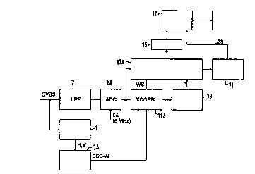
A preferred ~ L of the new WSS decoder concept is shown in
Fig. 5. Like the c.,..~. ' decoder, the new WSS decoder has means to select line 23 and
30 to generate some WSS related wmdows. It has also a buffer and interface. However, a PLL
is missing because a fixe~ frequency clock (5 MHz) is used. It contains an AID converter 9A
instead of the hard slicer 9 of Fig. 4, to make sofl decoding possible. Soft decoding is known
as such from A.M. Michelson and A.H. Levesque. "Error-control techniques for digital
" John Wiley & Sons, 1985, from T.R.N. Rao and E. Fujiwara, "Error-
wo s6ll3936 i ? ! ,~: 2 ~ 8 0 0 2 3 I ~ S~
control coding for computer systems," Prentice-Hall, 1989, and f}om J.G. Proakis, "Digital
" second edition, McGraw-Hill Book Co., 1989. rllLtl~ lulc, the
algorithms for word sync and data and data reliability estimation are much differently. Now,
let us focus m detail on this new concept.
The optimal low-pass filter 7 with respect to noise 1~ r.. , .. ~ is in this
case a replica of the elementary pulse that has been used at the encoder. E.g., its impulse
response is
h(t) = I/T . cos2 (~t/(2T)) for 'tl < T (I)
10 h(t) = 0 for ltl > T
where T = 200 ns. In practice this filter 7 is preceded by a video low-pass filter with a cut-
off frequency of about S MHz (B,G/PAL). The line 23 window generator 3A produces a
window ESC-W for an extended startcode ESC. This so called extended startcode ESC is the
15 tail of the run-m RI combined with the startcode SC (see Figs. 1,2) as explained in the non-
JIC, 1- ' ' ' ' '- I orrlirotinn WO-A-94/28678 (attorney's docket PHN 14,478), and
consists of 30 samples, i.e.
~c [ , , , +, +, +, , ,--, +, +, +, +,--,--,--, +, +, +, +,-- -- -- -- -- + + + + +] (2)
in binary notation, where "+" represents +1, and ~-" means -1. This extended startcode
ESC has better correlation properties th~m the startcode SC itself. The extended startcode
window ESC-W should be widened in order to include some timmg tolerance of the Hsync in
case of heavily disturbed channels with reference to horizontal timing (recording and replay
25 of VHS and SVHS recorders). As soon as the window rsc-w is active, the received signal
is cross-correlated with a replica of this extended startcode by an extended startcode cross-
correlator llA. Such a cross-correlation circuit llA is shown in detail as a part of Fig. 6.
The timing reference of WSS in line 23, i.e. word sync WS, is estimated by triggering on
that sample that results in the highest correlation peak (global maximum). The accuracy of
30 this estimate will be + 1/(2f,), where f, is the sample frequency, m case of a non disturbed
channel. E.g., in case of a S MHz clock, the UU~lhlUliy in the estimate will be + 100 ns.
T..~ i.. . Iike for instance linear or cubic, or use of a PLL instead of a fLxed clock can
i~nprove the accuracy of the tirning estimate. However, minor ilUIJIU.~ l.. in decoder
should be expected from an mcreased tt~ung accuracy because the input signal
2 1 ~023
W096/13936 ~ r~l,~._.c l~ --
is u~ ,d. Note that at this suge, it has not yet been detected whether we have WSS in
line 23 or not.
Now we have the timing relation, the dau bits are biphase code
5 ~ - ' ' by a biphase ~' ' ' and dau plus dau reliability estimator 13A to
produce the 14 bits and 14 violation flags. An RMS ~ . circuit 19
applies a threshold r to the ~' ~~ ' ' 13A on the basis of; ~f`~ received from the
cross-cûrrelator llA. A line 23 WSS detectiûn circuit 21 supplies the detection signal I~3 to
the interface 17 in response to ~ received from the ~ l 13A.
lû
The process of ~' ~ ' ' carried out by the ~ ' ' 13A is
shown in Fig. 7. Note that although single lines are shown, a multi-bit processing is
performed so as to imcrease the reliability by making an optimum use of the signal energy in
the WSS signal. Each biphase coded data bit consists of 6 bytes. The 6 bytes are separated
15 imto two nibbles of 3 bytes each. The sum of the bytes in each nibble is calculated. To this
end, the input bits are applied to a delay line of two delay cells 71, 73 each delaying over
the duration T of one byte. The input of the delay cell 71 and the outputs of the delay cells
71, 73 are applied to an adder 75. In accordance with the invention, any noise is reduced as
a ~ of this addition of mu~ti-bit data resulting in an integration of the energy in
2û the received data, whereby the accuracy depends on the number of bits assigned to each
sample by the A/D cûnverter 9A. Previously, a majority decision was carried out on three
successive sliced bits which is far less effective in ~ the effects of noise on the
reliability of the decoding process.
The data is estimated by subtracting the second nibble from the first
25 nibble. To this end, the output of the adder 75 is delayed over 3T by a delay circuit 77 and
inverted by an inverter 79. The outputs of the delay circuit 77 and the inverter 79 are applied
to an adder 81. The sign of the result is the dau estimate. To determine this estimate, the
output of the adder 81 is applied to a first logic circuit 83 which says that if the output
exceeds 0, the data bit dj is "1" while the dau bit is ro" in the other case. A second logic
30 circuit 83 deterrrlines a violation flag vi in response to the output of the adder 81. If the
output falls below the threshold r, the violation flag v; is "1", while the violation nag is ''û"
in the other case. Now, let us focus on how we make an estimation of the reliability of the
dau which process is shown in Fig. 6, in order to obtain the threshold r.
wo 96/13936 2 1 8 0 0 2 3 F._IIIL,~
Let us ret~rn to the point where we found the word sync WS. At that
pomt, we have a good match between the received extended startcode r,S~, and the replica
vcc, in the receiver. The received exoended stattcode can be modelled by the followmg
equation:
r~SC = s,sc + d (3)
where
- s,5~ = A.v,~ + C, where A represents the amplitude and C the common level,
10 and
- d is lC~Jl~C~ ui~, for the ~ in the channel which includes items like
- inter-symbol ;..t~ (ISI), noise, co-channel ~ (CCI), single carrier
i..,~ll;..l,ce, etc. CCI has been discussed in S. Dinsel and E. Sipek, "Frequency offset in
television - tneory and ~rrlir~tir~n," Reprinted from the EBU Review - Technical, No. 210,
15 April 1985.
How cam we derive an estimate of the ~ ? This can be achieved
by subtracting the replica from the received signal. Of course, the amplitude and the
common level should be estimated first before the subtraction can actually take place.
20 r~.. Ih~ , we take a DC-free subset of the extended startcode, which consists of 28
samples, in order to make the calculation of amplitude very simple, i.e.
V,,~Dc-f~ [,, ,+,+,+,-,-,-,+,+,+,+,-,-,-,t,+,+,+,-,-,-,-,-,+,+,+~ (4)
25 m binary notation. It appears that the last t~vo " + " symbols of the extended startcode given
in (2) are left out in (4). The amplitude, A, is estimated by applying the following for~nula:
A = ( VC~ DC-~ec r,S~ DC-~cc ) I 28 (5)
21 80Q23
WO 96113936 . _~1~ S. ~
The common level, C, is estimated by applying:
28
~ r,l~ dc-f~
28 ' ' " `"' ~~ ' ' " ' ' ' " ' ~
The replica that will be subtracted, is an estimate of thë received signal and is given by:
S = A Vac DC-fr~ + C (7)
The estimate of ~ lu~ .,e follows from:
d rac DC-f~ S (8)
10 A good estimate of the R~S dii~Lull is derived by:
28
~ Id,l (91
d = 28 ' '~
The quality of this estirnate of RMS ~ r can be expressed by its
probability density function (PDF) if the ' has a stochastic character. Knowledge
about the PDF of the d;."~l, ulce is not important accordmg to the central limit theory, as
15 long as the dj have the same PDF and are not correlated. The PDF of d is ~.., 'y a
Gaussian ~ ... with mean aldl amd variance aldl2l28 Note that ISI, which is alsointroduced by a timing error, will increase the RI~.S disturbance. The bigger the timing
error, the bigger the RMS .1.~1...l. 1. This is desirable.
If we assume that the major di~Lull,~uA,e will be added white Gaussian
20 noise (AWGN) then we can apply this knowledge mto ef~uation 9. As a result, we acquire
tne following ~
~ Id,l (10)
~ 28
where the mean and variance of estimate adG are related directly to the variance of the dj,
i.e., mean is equal to d and variance is 71'adZ/(2 28)
~~ 21 81:~023
wo 96/13936 r~.,~ . /n
11
At this poirlt, we have an estimate of the RMS ~ Lulb~ . From the
RMS iiD~ulb~ . the threshold level r is derived.
r = Z ~dG (ll)
s ..
where ad,G has been derived by using equation 10, and z is a constant. A good practical value
of z is 2. This threshold level is used to estimate the reliabiiity of each data bit, as is shown
in Fig. 7. If the absolute vaiue of a data sample is within tilis threshold level then the
c~ g violation flag is set else ti~is violation flag is reset. We have acquired at this
10 stage 14 data bits and 14 c.~. ''`l"""~; ~. violation bits.
Now we come to the pomt that we can answer the question: Is there WSS
in line 23 or not ? The following strategy is used. We count the number of violation flags.
Suppose that this number is equal to v. If v < n, where n is an element of {0, 1, ..., 7}
then WSS is detected in line 23 else not. A pMcticai value for n is 3. This WSS detection
15 strategy can be combined with a check on the parity of the aspect ratio bits.
In Fig. 6, the above theory has been , ' ' as follows. The multi-
bit output signal of the A/D converter 9A of Fig. S is applied to a proper cross-correlator 23
which includes a delay lirle of 29 delay cells T, .. T79, whose 30 taps correspond to the 30
20 symbols of the fuil extended startcode ESC. Cross-correlation is effected by inverting (by
means of inverters I1, I2, I3, ...) all taps wilich are supposed to suppiy negative symbols in
the extended startcode when the extended startcode is indeed there. An adder 27 sums 28
taps cu.r"~ , to the 28 symbols of the DC-free extended startcode, while an adder 25
sums 2 taps C~ ,D~ ' ~ to the remaining 2 symbols of the 30 symbol full extended25 startcode. An adder 29 sums the outputs of the adders 25, 27. A global maximum flnding
circuit 31, enabled by the extended startcode wmdow signal ESC-W, supplies the word sync
signai WS at the instant that the received string of symbols matches the symbol string of the
- extended startcode.
The amplitude A is obtamed in accordance with equation S by dividing the
3û output of the adder 27 by the vaiue 28 in a divider 33. Tile common level C is obtained in
~rrrn~7. rP with equation 6 by an adder 35 which sums the 28 taps of the delay line T, .. T2,
without inverting the taps ~ to the negative symbols in the extended startcode,
and a divider 37 which divides the output of the adder 35 by the value 28.
2180
W0 96113936 - 0 2 3 r~
12
The sum of the amplitude A and the common level C (see equation 7) is
subtracted from the 28 taps of the delay line T, .. T~, (see equation 8) by subtracters S, .~
S~8, whose outputs are applied to respective absolute value ~i ~ .. ~Y circuits AVI .. AV25
to obtain the ldjl values in equatiorl 9. These ¦di¦ values are summed by an adder 39, whose
5 output is applied to an arithPIetic circuit 41 to obtain ad,G in accordance with equation 10.
The output of the arithmetic circuit 41 is applied to a buffer 43 which is o~ .lllUlfl~;l by the
word sync signal WS.
In this section we showed and explained in detail a preferred ' ~ '
of a new concept WSS decoder. A high accuracy and a reduction of noise are obtained thru
10 the shown mtegration of tne energy in the multi-bit signals irlstead of by using simply sliced
signals. IAhe d ~ ...;.. ';.. of the .li,i...l,~.~e as illustrated in Fig. 6 results in a very useful
indication of the reliability of the received data, as for each data bit di, a violation flag v, is
fi~r~T7ninrd in ~ upon the determined .~
15 4. Extension of the new WSS decoder: Cirr~ for Protection aYainSt FM-clicks or sPike
noise
Let us start by explaining how an FM-click (or spike noise) can disturb a
WSS signal. In Fig. 9 an exa~ple is given. It shûws an FM-click FMC which affects bit no.
20 9 of the WSS signal (so~id curve). The i ~ that is supposed to be transferred by bit
no. 10 is a 1 (dashed curve). If we apply low-pass filtering and proceed with biphase code
' ' then it is shown by Fig. 10 that a 0 (solid curve) is estimated at the receiver
instead of the i ' I (dashed curve). If the received sigrlal is not or minor disturbed
by other kinds of , then the l;-l -i-~ threshold level is very small. Hence, it is
2'i likely that this error is not marked with a vioiation nag and therefore can cause , UIJlid~:,
switching m the TV receiver. We like to have means to prevent tbis i...,Jll, switching.
A block schematic of an . ' that can detect, or better mark,
the occurrence of an FM-click, is shown in Fig. 8. Its operation will be explained with help
of the example in Figs. 9, 10 and 11. First, the data bit, which is in this example data i~it
30 no. 9, is estimated (see Fig. 10), just like in the ' ' of Fig. 7. This data estimation
result d; is fed to inputs I1 of the FM-click detector 87. From the biphase ~ ' ' , two
results (output and inPut of the delay circuit 77, I.,~ .,lr) are fed to inputs
12 of the upper and lower box 89, 91 of the FM-click detector 87 l~o~ r~ These two
results c m be regarded as the u(Jll~*Julllli. g results of amplitude summation
r ~
2 1 80023
WO 96/13936
13
(integration of energy) of the two half symbols whuch make the biphase code. ln this
example, data bit no 9 has been estimated as a 0, so Il = 0. Therefore, the FM-click
detector 87 will proceed with the following tests (i.e. the else parts of the logical statements
im the boxes 89, 91):
S
- If the first i~ -~~ result I2 (output 77) is greater than HL (}ugh level) then
the upper box 89 outputs a 1 else 0. Result in this example: l.
- If the second ' result I2 (input 77) is less than LL (low level) then
the lower box 91 outputs a 1 else 0. Result in this example: 0.
In this example, one of the two boxes in the FM-click detector outputs a 1. This meAns that
an OR circuit 93 receivmg the outputs of the upper and lower boxes 89, 91 of the click
detector 87 and the output of the logical circuit 85 has at least one " 1 " input, so that
violation flag no. 9 will be set which marks bit no. 9 as being unreliable.
In the , '~ HL and LL have been chosen equal to 3(C + A12)
and 3(C - A/2) lGD~ ArhiS is not strictly required but preferred.
In the next sections we proceed with simulation and . - ~ results
on the ~,.r.,llll~lce of the new concept WSS decoder.
20 5. Sim--lAt-~i DerfDrm?nr~ of the rirrrrir~r
The block schematics of Figs. 5, 6 and 7 have been i.. l,l.. ~ ~1 in a
simulation model. Some graphicAI results frDm this model are presented in Figs. 12. 13 and
14 which show l~ .,Li~.,ly the eye pattern of a WSS signal, the ~ estimation and25 the data and data reliability estimation prDcess with the use of a threshold level. Note from
Fig. 13 that the di~L~I/~ , estimate (indicated by ~D) is sensitive to the timmg jitter or
timing tolerance which causes ISI. The arrows P indicate the peaks due to timmg jitter (or
tolerance).
The ~ r of the new concept WSS decoder is simulated for an AWGN
30 chcumel only. The ~. ' is expressed by two 1,l.,l. '. ~;~;. ~
1. The probability that Ime 23 WSS will be rejected: P[reject].
2. The probability of a bit error in one specific WSS bit: P[bit error].
2 1 80023
W0 96/13936 I ~ ~,'.'C .
14
Both ~.ul.~ilili~ will be presented versus the signal-to-noise ratio (SNR).
The SNR is defined in appendix A. Fig. 15 shows the ~ versus SNR (course
timing estimate). The vertical axis gives the probability P, while the horizontal axis gives the
picture signal-to-noise ratio SNR in dB. In the drawings, PIr] indicates P[reject], while P[be]
5 indicates P[bit error]. In Fig. 15 the result of the ' is sbown by the "x" symbols.
Due to the amount of r^' ' ' I effort, Plreject] has been derived from the ~
only. A probability of P[reject] = 1/2 is .o c~ at about 8 dB SNR. This figure is a
practical measure of the lower limit of SNR at wbich the decoder still decodes the WSS
i~' quite fast. Below th~is figure, the p.,.ru~ ll.c (and speed~ of the WSS decoder
10 will decrease very fast.
The solid, dash-dotted, dotted and dashed lines in Fig. 15 give the
calculated values of P[reject], 1 - P[reject], P[bit error] and P[bit error]/(l - P[reject])
ly, which are derived from a ~ h- - --;- ,-1 model which will not be hi~hli~htPd in
this ~Pcrrirtinn
The "o" and -~\r symbols give the measured ~.. r.. - - f of the new
concept WSS decoder of P[reject] and Plbit error] (and P[bit error] / (1 - P[rejeci]) )
c~ ly. The difference of about 3 dB between the simulated result and the measured
results in favor of the simulation results, is, r ' - 1~ due to the use of a low-pass filter
with a cut-off frequency of 1 MHz insoead of an ideal filter as mentioned in section 3.
~0 However, the cunes seem to have a constant difference of 3 dB versus SNR which makes it
assumable that adjustment of this filter would solve the difference. This has been verified
recently.
In Fig. 16 the L~ r.,....~. ~ of a new concept WSS decoder which uses
cubic il~ iul~ in order to improve the timing estimate (fractional timing estimate), is
25 shown versus the SNR. The "x" symbol represents the simulation result of P[reject]. The
different ~,, r curves are frotn a ' ' model. If we compare the ~,. . r~ -,. f
in case of fine timing (hl;~ )UL~ JII) versus coarse timing, we see that at P[reject] = 112
there is a difference of about 0.5 dB in favor of ftne timing. We can ask ourself the
following question: Is a 0.5 dB , ~ in l c~ enough basis for the cost of
30 extra hardware ?
:` ~ 2180Q23
W0 96113936 ` ~ r~
6. Measured F~- r~ n ~ of the decoder
In the previous section, the measured ~ rulllla~ of the new WSS
decoder has already been presented with respect to noise (see Fig. 15). In this section we
S focus on ~,.,lrullllall.e results with respect to other kinds of ." ' than noise.
Here below, a summary of .,.~ .. results is given for different kind
of ~li~...lll,.,ll,,.,~.
- Echoes.
The maximum permitted level is about ~ dB to -9 dB, which figure is highly
dependent on the delay of the echo and the p r~ .. ~ of the sync separator.
- Co-channel ihl.l If~,l~,l.l,~ (CCI).
The maximum permitted level of CCI is rlpt~rminrd by the 1 r~ of the
sync separator only.
- Single carrier ;- ' f ~ r
Single carrier; t` ~ ~ ~ with a frequency offset of 867 kHz with regard to
vision carrier has been added to the chanrlel. T-.t` . f~ c ~ ~ with that frequency of
867 kHz is a worst case choice (see the PSD of the WSS signal in Fig. ~) In
case of no WSS signal in line 23, we could not switch on the WSS decoder
even at arL r level of +10 dB with regard to the vision carrier.
In case of single carrier ihl~ lcll~ with the same frequency offset as above
but with a WSS signal in line 23, the decoder first failed at a level of -2 dB
with regard to the vision carrier.
- VHS and SVHS video recorders (VCR).
The WSS decoder has been tested with several replays of VHS and SVHS
which included also i channels, and also with replays of
copies of those recordings. Multiple parameters were tuned during replay, of
which the most important are sharprless control and trackin~ r ~,' ' The
decoder could decode with average to high ~_lr~ all replays except for
some that had a non-lc~.ul_labl~ failure in that sense that line 23 had oeen
shifted to another line.
WO96/13936 2 1 8~3 "~" 5~
16
From the results above and ~ ; in the field, we know that this
WSS decoder is insensitive for low (and high) frequency distortions like line tilt, satellite
dispersal (25 Hz), low frequency i~....r.,lc~ tc. '~rhe reason is that biphase code
.I....r~ ;..-- is applied in the decoder so tilat the actual data samples are freed from low-
5 frerluency c.~ The biphase code ~' ' ' implies that no slicer circuit has to beincluded. This slicer has means to f nd a voltage level of half the data top-top amplitude in
order to perform well. Such a slicer is very sensitive to low frequency distortions.
7. onclusions
C . .. _ . .. . . .. .
We have shown a new concept of a wide screen signalling decoder. The
approach that has been used differs much from r ~. ' decoders. The kernel of this
new concept WSS decoder exists of a cross correlation technique for word sync, biphase
code ~l. "o~ ;"l~ and a data and daia reliability esti~iation technique which makes use of an
15 RMS ~ ull,~.l.e threshold. /rhe ~ ' of those tiiree techniques in the new concept
WSS decoder has shown to be very robust against all kinds of .liDl..~b~..,i. which are
.~ ~d in the television channel, including the replay of recordings of VHS and SVHS
video recorders.
20 Appendix A: I~efinition of Si~n~l-to-Noise Ratio
In relation to the composite video baseband signal (CVBS), there are
several definitions of picture signal-to noise ratio (SNR). Withrn the context of this
diælosure, we define the picture signal-to-noise ratio as the unweighed picture signal-to-noise
25 ratio over a vision bandwidth of 5 MHz (B,GIPAL). E.g.,
SN~ = lO log ~ (0 7 Volt)2 1 (A1)
l I r, N(f)df J
where
- 0.7 Volt is the difference in ainplitude of peak white and black level in the
CVBS.
- Vision bandwidth B~ = 5 MHz.
- N(fl is the one sided power spectral density of the noise in the CVBS.
W096113936 ~ ' 2 1 8 ~ 2 .~
The relation between the SNR and the vision carrier-to-noise ratio (CNR)
has been discussed ~.A~ y in A.P. Robinson, "The ' , between vision carrier-
to-noise ratio and picture signal-to-noise ratio in a system I television receiver", Technical
Report 1987123, BBC Research Dep~-nt UK, 1987, for system I/PAL television
5 receivers. For system B,G/PAL television receivers this relation is somewhat different, and
is giYen by:
CNR = SNR + 6.8 dB (A2)
10 where the noise power spectral density is assumed to be flat in the concerning frequency
band. The relation between the SNR and the antemla input volhge is dependent on the type
of tuner that is used (noise figure). An example of picture SNR in dB versus antenna input
volhge level in dB~LV is shown in Fig. 17.
It should be noted that the above-mentioned ~ l ' illustrate rather
than limit the invention, and that those skilled in the art will be able to design many
alternative, ~ ' without departing from the scope of the appended claims. For
example, the described method of decoding a WSS signal of a PALplus television signal can
also be used to decode more reliably a VPS signal. The described method can further be
2Q used for decoding any otber dah signal having at least a shrtcode or sync word section and a
dah section. More specifically, an NRZ-coded teletext signal (17rl) can a.l~ / be
decoded in accu.d~ with claim 11. In the claims, any reference signs placed between
shall not be construed as limiting the claim. The invention can be ;.. .1,l. . ,t.
by means of hardware . , ~ several distinct elements, and by means of a suitably25 I!JlU~l~lllI...;:d computer. The invention is ad~ u~l.~ applied in a video signal receiving
apparatus (e.g. a television set or a video recorder) for processing a video signal including a
dah signal portion, which apparatus comprises in addition to the A/D converter 9A, the
cross-correlation circuit llA, the RMS d;-~ - circuit 19, and the code
~' ' ' - 13A, video signal processing circuitry for processing tbe video signal in
.l. ~.. l. c upon the ' ' ' dah signal to obhin a processed video signal which cam
be displayed on a display device (e.g. a CRT) or recorded by a recûrding .. l~ . in a
video hpe recorder. For eAample, the video signal processing circuitry may operate in
,....l..,. c upon the aspect ratio bits 3210 to switch between video signal processing of a
Wo 96/13936
~:3 signal and video signal processing of a 16:9 signal, with any ~,VII~a~lVlldi~g
of tbe deflection, such as available in current 16:9 aâpect ratio receivers.