Sélection de la langue

Search

Sommaire du brevet 2181635 

Énoncé de désistement de responsabilité concernant l'information provenant de tiers

Une partie des informations de ce site Web a été fournie par des sources externes. Le gouvernement du Canada n'assume aucune responsabilité concernant la précision, l'actualité ou la fiabilité des informations fournies par les sources externes. Les utilisateurs qui désirent employer cette information devraient consulter directement la source des informations. Le contenu fourni par les sources externes n'est pas assujetti aux exigences sur les langues officielles, la protection des renseignements personnels et l'accessibilité.

Disponibilité de l'Abrégé et des Revendications

L'apparition de différences dans le texte et l'image des Revendications et de l'Abrégé dépend du moment auquel le document est publié. Les textes des Revendications et de l'Abrégé sont affichés :

  • lorsque la demande peut être examinée par le public;
  • lorsque le brevet est émis (délivrance).
(12) Brevet: (11) CA 2181635
(54) Titre français: CIRCUIT DOTE D'UN MULTIPLEXEUR
(54) Titre anglais: CIRCUIT ARRANGEMENT WITH A MULTIPLEXER
Statut: Périmé et au-delà du délai pour l’annulation
Données bibliographiques
(51) Classification internationale des brevets (CIB):
  • H04J 3/02 (2006.01)
  • H03F 3/45 (2006.01)
  • H03F 3/72 (2006.01)
(72) Inventeurs :
  • BECHER, ERWIN (Allemagne)
(73) Titulaires :
  • ENDRESS + HAUSER WETZER GMBH + CO. KG
(71) Demandeurs :
  • ENDRESS + HAUSER WETZER GMBH + CO. KG (Allemagne)
(74) Agent: SMART & BIGGAR LP
(74) Co-agent:
(45) Délivré: 2000-03-07
(22) Date de dépôt: 1996-07-19
(41) Mise à la disponibilité du public: 1997-01-30
Requête d'examen: 1996-07-19
Licence disponible: S.O.
Cédé au domaine public: S.O.
(25) Langue des documents déposés: Anglais

Traité de coopération en matière de brevets (PCT): Non

(30) Données de priorité de la demande:
Numéro de la demande Pays / territoire Date
95 11 2054.2 (Office Européen des Brevets (OEB)) 1995-07-29

Abrégés

Abrégé français

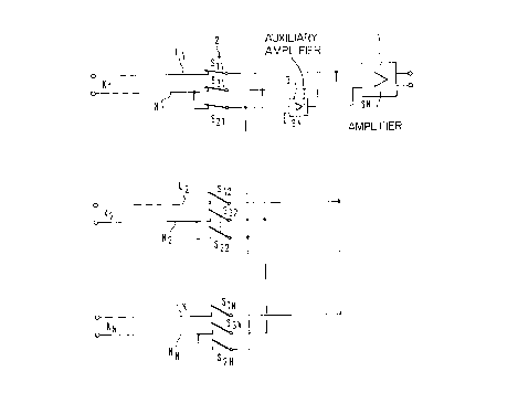
Pour connecter un de N canaux de signaux (K1, K2, KN) ayant chacun une ligne de signal (L1, L2, LN) et une ligne de zéro du signal (N1, N2, NN), où N est supérieur à un, à une entrée d'un amplificateur (différentiel) (1) dont le circuit est référencé à une terre associée (SN), un-de-N multiplexeur (2) est fourni ayant 3N voies de commutation (S11, S21, S31, S12, S22, S32, S1N, S2N, S3N), dont une première (S11, S12, S1N) sert à connecter les N lignes de signal (L1, L2, LN) à ladite entrée, et dont une seconde (S21, S22, S2N) sert à faire progresser les N lignes de zéro de canaux (N1, N2, NN). Les entrées respectives des voies de commutation d'une troisième série de voies de commutation (S31, S32, SN) sont connectées aux entrées respectives des voies de commutation de la deuxième série de voies de commutation (S21, S22, S2N), et les sorties de ces dernières sont réunies à une entrée d'un amplificateur auxiliaire (différentiel) (3). Les sorties de la troisième série de voies de commutation (S31, S23, S2N) sont réunies à la sortie de l'amplificateur auxiliaire (différentiel), dont le circuit est référencé à la terre (SN) de l'amplificateur (différentiel) (1).


Abrégé anglais

To connect one out of N signal channels (K1, K2, KN) each having a signal line (L1, L2, LN) and a channel zero line (N1, N2, NN), where N is greater than one, to one input of a (differential) amplifier (1) whose circuit is referenced to an associated ground (SN), a one-out-of-N multiplexer (2) is provided having 3N switching paths (S11, S21, S31, S12, S22, S32, S1N, S2N, S3N), a first (S11, S12, S1N) of which serves to connect the N signal lines (L1, L2, LN) to said input, and a second (S21, S22, S2N) of which serves to advance the N channel zero lines (N1, N2, NN). The respective inputs of the switching paths of a third switching-path set (S31, S32, SN) are connected to the respective inputs of the switching paths of the second switching-path set (S21, S22, S2N), and the outputs of the latter are commoned to one input of an auxiliary (differential) amplifier (3). The outputs of the third switching-path set (S31, S23, S2N) are commoned to the output of the auxiliary (differential) amplifier, whose circuit is referenced to the ground (SN) of the (differential) amplifier (1).

Revendications

Note : Les revendications sont présentées dans la langue officielle dans laquelle elles ont été soumises.


- 7 -
C L A I M S
1. A circuit arrangement for a single-terminal through-
connection of one out of N signal channels each
comprising a signal line and a channel zero line, where N
is greater than one, to an input of an amplifier whose
circuit is referenced to an associated ground, using a
one-out-of-N multiplexer having 3N switching paths,
- a first switching-path set serving to connect through
the N signal lines,
- a second switching-path set serving to advance the
N channel zero lines,
- the respective inputs of the switching paths of a
third switching-path set being connected to the
respective inputs of the switching paths of the
second switching-path set,
- the outputs of the second switching-path set being
commoned to an input of an auxiliary amplifier, and
- the outputs of the third switching-path set being
commoned to the output of the auxiliary amplifier,
-- whose circuit is referenced to the ground of the
amplifier.
2. A circuit arrangement as claimed in claim 1 wherein
the amplifier and the auxiliary amplifier are each
implemented with a differential amplifier having one of
its inputs connected to the ground of the amplifier.

Description

Note : Les descriptions sont présentées dans la langue officielle dans laquelle elles ont été soumises.


2181635
Wt 4 CA
Circuit Arrangement with a Multiplexer
FIELD OF THE INVENTION
The present invention relates to a circuit arrangement
for connecting a plurality of signal lines to an input of
a differential amplifier by means of a multiplexer.
BACKGROUND OF THE INVENTION
Such circuit arrangements are needed, for example, if
signal channels which carry signals originating from
several measuring points with suitable sensors are to be
alternately or successively connected to the input of a
differential amplifier. Each signal channel generally has
a signal line and a channel zero line.
The channel zero line need not necessarily be connected
to ground, as in the case of a battery, for example,
where the signal line and the channel zero line serve to
connect the two terminals of the battery to desired
points of a circuit.
Normally, the multiplexer serves to connect both the
signal line and the channel zero line to the differential
amplifier; thus, a two-terminal through-connection is
made.
Mo/Ke/Lo
17.06.96

2181635
SUMMARY OF THE INVENTION
However, problems are caused by the fact that the
individual channel zero lines may be affected by
interference voltages, which depend in particular on the
type and place of the ground to which the respective
channel zero line is connected, and on the distance
between that place and the differential amplifier, i.e.,
generally on the length of the channel zero line. The
channel zero lines may also carry interference currents
which result in equivalent interference voltages, for
which comparable considerations apply.
Since, in addition, the interference voltages may have
different amplitudes from signal channel to signal
channel, the input of the differential amplifier to which
the channel zero lines are connected is fed with voltages
which differ from one signal channel to another.
Therefore, the output of the differential amplifier has
different interference components, particularly zero
offsets, and unacceptable compensating currents flow at
the input end of the differential amplifier.
The problem described is particularly disturbing if the
output signal from the differential amplifier is to be
further processed, e.g., if the signal is to be made
visible or recorded by means of readout equipment,
particularly a chart recorder.
Attempts have been made to solve the problem by
electrically isolating the differential amplifier and the
signal channels from each other, e.g., by means of
transformers or optocouplers. This, however, is

2 1 ~1 635
expensive, particularly if a great number of signal
channels are present.
To solve the problem described, the invention provides a
circuit arrangement for a single-terminal through-
connection of one out of N signal channels each
comprising a signal line and a channel zero line, where N
is greater than one, to an input of an amplifier whose
circuit is referenced to an associated ground, using a
one-out-of-N multiplexer having 3N switching paths,
- a first switching-path set serving to connect through
the N signal lines,
- a second switching-path set serving to advance the
N channel zero lines,
- the respective inputs of the switching paths of a
third switching-path set being connected to the
respective inputs of the switching paths of the
second switching-path set,
- the outputs of the second switching-path set being
commoned to an input of an auxiliary amplifier, and
- the outputs of the third switching-path set being
commoned to the output of the auxiliary amplifier,
-- whose circuit is referenced to the ground of the
amplifier.
In a preferred embodiment of the invention, the amplifier
and the auxiliary amplifier are each implemented with a
differential amplifier having one of its inputs connected
to the ground of the amplifier.
One advantage of the invention is that only the signal
lines are connected through to the input of the amplifier
or differential amplifier, while the interference

21~1 b35
-
-- 4 --
voltages on the channel zero lines are compensated for by
means of the auxiliary amplifier or auxiliary
differential amplifier, the latter having its other input
connected to the ground of the amplifier. Therefore,
mutual interference between the individual signal lines
is also suppressed. Thus, unlike the above-explained two-
terminal through-connections, the invention proposes a
single-terminal through-connection.
BRIEF DESCRIPTION OF THE DRAWING
The invention will now be explained in more detail with
reference to the single figure of the accompanying
drawing, in which the principle underlying the invention
is illustrated schematically in the manner of a block
diagram with the aid of an embodiment.
DETAILED DESCRIPTION OF THE DRAWINGS
Of N signal channels, where N is greater than one, three
are shown in the figure, namely signal channels K1, K2, KN.
Each of them has a respective signal line L1, L2, LN and a
respective channel zero line N1, N2, NN-
The signal lines and the channel zero lines establish the
connections with respective signal sources, e.g., with
respective measuring points each comprising a suitable
physical-to-electrical transducer, e.g., a so-called
sensor. The signal lines and the channel zero lines may
have arbitrary lengths, which is illustrated in the
figure by portions thereof shown as broken lines.

- ~8163~
Each of the channel zero lines N1, N2, NN may be connected
to a separate ground associated, for example, with the
aforementioned measuring point, as was explained by way
of introduction, but this is not shown in the figure.
By means of a one-out-of-N multiplexer 2, one of the N
signal channels K1, K2, KN can be connected to an
amplifier 1 at a time. To this end, the one-out-of-N
multiplexer 2 has 3N switching paths S11, S21, S31, S12, S22,
S32, S1N~ SSN~ S3N~ which can be thought of as grouped into a
first switching-path set consisting of switching paths
S11/ S12~ S1N~ a second switching-path set consisting of
switching paths S21, Sæ, S2N~ and a third switching-path
set consisting of switching paths S31, S32, S3N-
In the figure, the one-out-of-N multiplexer is shown
implemented with a mechanical switch. It is, however,
within the scope of the invention to implement the
switching paths and their control with electronic
switches, particularly with semiconductor switches.
To illustrate the operation of the one-out-of-N
multiplexer 2, the switching paths S11, S21, S31 associated
with the first signal channel K1 are shown closed, while
the other switching paths are shown open.
The first switch-path set S1l, S12, S1N serves to connect
the N signal lines L1, L2, LN to one input of the amplifier
1, whose circuit is referenced to an associated ground
SN. The second switching-path set S21, Sæ, SSN serves to
advance the N channel zero lines N1, N2, NN-
To this end, the respective inputs of the switching paths
S31, S32, S3N f the third switching-path set are connected

21~;6:~5
to the respective inputs of the switching paths S21, S22,
S2N Of the second switching-path set, while the outputs of
the latter are commoned to one input of an auxiliary
amplifier 3. The circuit of the latter is also
referenced, or connected, to the ground SN of the
amplifier 1. The outputs of the third switching-path set
S31~ S32~ S3N are commoned to the output of the auxiliary
amplifier 3.
Thus, through the "short circuit" between the output and
input of the auxiliary amplifier 3, the potential of the
ground SN is applied to the multiplexer-input-side end of
the respective channel zero line N1, N2, NN after each
switching step of the one-out-of-N multiplexer 2.
Accordingly, the above-mentioned compensating currents
and/or offsets cannot adversely affect the output fo the
amplifier 2, and in contrast to the above-described two-
terminal through-connections to a differential amplifier,
only a single-terminal through-connection to the
amplifier 1 is provided.
The amplifier 1 and the auxiliary amplifier 3 are shown
-in the figure of the drawing as differential amplifiers,
which implementation is preferred.
As briefly mentioned above, the signal appearing at the
output of the amplifier 1 can be recorded and/or made
visible in analog or digital form by means of readout
equipment, such as a chart recorder or a liquid-crystal
display. The subject matter of the invention is thus
preferably part of such readout equipment. If the output
signal is recorded or displayed digitally, the amplifier
1 must be succeeded by an analog-to-digital converter.

Dessin représentatif
Une figure unique qui représente un dessin illustrant l'invention.
États administratifs

2024-08-01 : Dans le cadre de la transition vers les Brevets de nouvelle génération (BNG), la base de données sur les brevets canadiens (BDBC) contient désormais un Historique d'événement plus détaillé, qui reproduit le Journal des événements de notre nouvelle solution interne.

Veuillez noter que les événements débutant par « Inactive : » se réfèrent à des événements qui ne sont plus utilisés dans notre nouvelle solution interne.

Pour une meilleure compréhension de l'état de la demande ou brevet qui figure sur cette page, la rubrique Mise en garde , et les descriptions de Brevet , Historique d'événement , Taxes périodiques et Historique des paiements devraient être consultées.

Historique d'événement

Description Date
Le délai pour l'annulation est expiré 2014-07-21
Lettre envoyée 2013-07-19
Inactive : CIB de MCD 2006-03-12
Lettre envoyée 2002-09-20
Lettre envoyée 2002-06-28
Lettre envoyée 2000-07-06
Accordé par délivrance 2000-03-07
Inactive : Page couverture publiée 2000-03-06
Inactive : Taxe finale reçue 1999-12-08
Préoctroi 1999-12-08
Lettre envoyée 1999-11-04
Un avis d'acceptation est envoyé 1999-11-04
Inactive : Approuvée aux fins d'acceptation (AFA) 1999-10-18
Modification reçue - modification volontaire 1999-03-12
Inactive : Dem. de l'examinateur par.30(2) Règles 1998-11-16
Inactive : Renseign. sur l'état - Complets dès date d'ent. journ. 1998-05-05
Inactive : Dem. traitée sur TS dès date d'ent. journal 1998-05-05
Demande publiée (accessible au public) 1997-01-30
Toutes les exigences pour l'examen - jugée conforme 1996-07-19
Exigences pour une requête d'examen - jugée conforme 1996-07-19

Historique d'abandonnement

Il n'y a pas d'historique d'abandonnement

Taxes périodiques

Le dernier paiement a été reçu le 1999-06-23

Avis : Si le paiement en totalité n'a pas été reçu au plus tard à la date indiquée, une taxe supplémentaire peut être imposée, soit une des taxes suivantes :

  • taxe de rétablissement ;
  • taxe pour paiement en souffrance ; ou
  • taxe additionnelle pour le renversement d'une péremption réputée.

Veuillez vous référer à la page web des taxes sur les brevets de l'OPIC pour voir tous les montants actuels des taxes.

Titulaires au dossier

Les titulaires actuels et antérieures au dossier sont affichés en ordre alphabétique.

Titulaires actuels au dossier
ENDRESS + HAUSER WETZER GMBH + CO. KG
Titulaires antérieures au dossier
ERWIN BECHER
Les propriétaires antérieurs qui ne figurent pas dans la liste des « Propriétaires au dossier » apparaîtront dans d'autres documents au dossier.
Documents

Pour visionner les fichiers sélectionnés, entrer le code reCAPTCHA :


Pour visualiser une image, cliquer sur un lien dans la colonne description du document. Pour télécharger l'image (les images), cliquer l'une ou plusieurs cases à cocher dans la première colonne et ensuite cliquer sur le bouton "Télécharger sélection en format PDF (archive Zip)" ou le bouton "Télécharger sélection (en un fichier PDF fusionné)".

Liste des documents de brevet publiés et non publiés sur la BDBC .

Si vous avez des difficultés à accéder au contenu, veuillez communiquer avec le Centre de services à la clientèle au 1-866-997-1936, ou envoyer un courriel au Centre de service à la clientèle de l'OPIC.


Description du
Document 
Date
(aaaa-mm-jj) 
Nombre de pages   Taille de l'image (Ko) 
Page couverture 1996-10-22 1 16
Abrégé 1996-10-22 1 29
Revendications 1996-10-22 1 32
Dessins 1996-10-22 1 11
Description 1996-10-22 6 221
Page couverture 2000-02-01 1 38
Dessins 1999-03-12 1 12
Dessin représentatif 1997-08-22 1 8
Dessin représentatif 2000-02-01 1 5
Rappel de taxe de maintien due 1998-03-23 1 111
Avis du commissaire - Demande jugée acceptable 1999-11-04 1 164
Avis concernant la taxe de maintien 2013-08-30 1 171
Correspondance 1999-12-08 1 36
Correspondance 2002-06-28 1 7
Correspondance 2002-09-20 1 8
Taxes 1999-06-23 1 38
Correspondance 2000-07-06 2 58