Note : Les descriptions sont présentées dans la langue officielle dans laquelle elles ont été soumises.
~ 2181843
DEMODULATOR, MODULATION AND DEMODULATION SYSTEM,
AND DEMODULATION METHOD
BACKGROUND OF THE INVENTION
l. Field of the Invention
The present invention relates to a demodulator for
recovering a required signal by accomplishing quadrature
detection of a received signal carried on a high-
frequency carrier wave.
2. Discusslon of the Related Art
Fig. 17 illustrates a conventional quasi-coherent
quadrature detector which is described in the technical
report of CS87-109 of the InstLtute of Electronics.
Information and Communication Engineers of Japan,
entitled "A study of the demodulation mathematics for a
signal which has been subJect to phase-shif~ keying".
In Fig. 17, the conventional quasi-coherent
quadrature detector is comprised of a first mixer 1 for
mixing a received IF signal with the output signal of a
fixed oscillator 3, a second mixer 2 for mixing the
received IF signal with a ,~/2 phase-led signal from the
phase of the output signal of the fixed oscillator 3, the
fixed osclllator 3 whose output frequency is
approximately equivalent to the center frequency of the
received IF signal, a phase shifter 4 for shifting the
2181843
phase of the output signal of t~le fixed oscillator 3 by
~/2 ahead, a first low-pass filter 5 (hereinafter
referred to as LPF) for eliminating harmonic compon~nts
of the output of tlle first mixer 1, a second LPF 6 for
eliminating harmonic components of t~le output of the
second mixer 2, a first analog to digital (hereinafter
referred to as A/D) converter 7 for performing A/D
conversion of tlle output of the first LPF 5, a second A/D
converter 8 for performing A/D conversion of t~le output
of tlle second LPF ~, input terminals 9 for a clock signal
for clocking the first A/D converter 7 and the second A/D
converter 8.
Now, the operatLon of the conventional quasi-
coherent quadrature detector illustrated in FLg. 17 will
be described. It is assumed herein that a received IF
signal is p~lase-modulated and is calculated by tZle
followLng equation:
I~(t) = Re[(l(~ jQ(t)) eXP {j(~l) ct ~- ~ c }]
= /(t)Cos(o)C~ +~c)-Q(t)sin(u)ct ~-~c)
=~ )COS{~I)Ct+~3c~ (t)}
where
(t) cos{~ )} ~ (2)
Q(t) = ~(t)sin{~ )}
2181843
w~lere I(t) represcnts an Ln-p~lase baseband
componcnt, Q(t) represents a quadrature-phase baseband
component, ''~c represents a carrier angular frcquency,
C (t) represents a carrier pllase, A(t) represents a
carrier amplitude component, and ~ (t) represents a
modulated phase component.
For the simplified description, it is also assumed
herein that the frequency of t~le output of tlle fixed
oscillator 3 is equal to the frequency ~c of the received
IF signal.
Lo(~) = 2cos((~)ct ~ Lo) (3)
L p (1) = -2 si n((J) ct ~- ~ Lo ) (4)
where Lo (t) represents the output signal of t~le
fixed oscillator 3, Lp (t) represents the output signal of
the phase shift~r 4. ~Lo represents the initial phase of
tile output signal of the fixed oscillator 3. In this
situation, an output signal Ml (t) of the first mixer l is
represented by tllc following Equatlon (5) and an output
signal M~ (t) of the second mixer 2 is represented by the
following Equation (6):
ML(~) = R(~) x Lo(~)
= ~(t)[cos((~ c ~ ~ Lo ) t- ~ "~ (~)} + cos{2(" ~ t (~ c t (3 Lo ) + ~ )}]
= .4(/)[cos{~ r +~ )}+C5{2(J)C +~P +~/r~ ] (S
r~
21818~3
M2(1) = R(l) x Lp(l)
=,4(1)~sin{(~c-n~,0)1O",(l)~-sin{2(1~c 1( ~ 1n~,O)1o",(/)}]
= ~(/)[sin{~ ",(/)} ~1~1{2~JlC ~ 1~0 /' t 11",(1)~] (f~ j
where A~N represents ~C ~ t3~1p A~p r~presents C f ULo.
The output si~nal M1 (t) of the first mixer l and the
output signal M2 ( t) of the second mixer 2 are Lnput into
the first LPF and the second LPF respectively for tlle
elimination of harmonic components, and quasi-coherent
detected slgnals IQC (t) and r~QC (t) are obtained.
IQC (~ ) cos {~ l,r + ~ ,n (/ ) } l ( 7 )
QC(~ (/)sin{~ r~ )}
W1len the quasi-coherent detected signals in Equation
(7) are expressed in terms of complex numbers, the
following Equation (8) is obtained:
QC ( ) ( ) P { j( I~ n~ ( ))}
) exp (j~ m (t )~ exp(j~
2 0 = .,4 ( t ) (CoS (3 ~ j s i n (3 rrl (~ )} eX p (~
= {I(t) + jo(t)}exp(j~ r ) (8)
As a result of quasi-coherent detection, it is found
that the quasi-coherent detected output can be obtained
by phase-rotating a transmitted baseband signal by ~
~ 2181843
which is a phase difference between the received IF
signal and the output signal of the î ixed oscillator 3 .
Then, the quasi -coherent detected signal IQC ( t ) of
the first LPF and the quasi-coherent detected signal QQC
(t) of the second LPF are converted into digital signals
through the first A/D converter 7 and the second A/D
converter R respectively.
The quasi-coherent detected signals which have becn
converted by the A/D converters undergo demodulation such
as coherent detection and differential detection at the
subsequent steps of operation. When the frequency of the
recelved IF signal and the frequency of the output slgnal
of the flxed oscillator 3 are different, the phase-
rotated ~N should only be changed to (~C ~ ~L0) t + ~N~
and the slmilar slgnal processlng to that described above
is applicable. The operation principles of the
conventional quasi-coherent quadrature detector are as
described above.
The conventional quasi-coherent detector portion of
the demodulator for accomplishing quadrature detection
prior to A/D conversion is comprised of analog circuits
as described above. Consequently, the conventional
quasi-coherent detector has the following disadvantages:
1) An amplitude deviation occurs between IQC (t) and
QQC ( t ) .
-
- 2lsla43
2) A direct-current offset occurs ln the A/D
converters .
3) Accuracy for accomplishing quadrature detection is
insufficiently provided.
SUlv~lARY OF T~E INVENTION
The present invention is made to solve the above-
described problems. It is therefore an ob,~ect of the
present invention to provide a demodulator having a
quadrature detector with improved accuracy for
accomplishing quadrature detection, being free from an
amplitude deviation and a direct-current offset by means
of the simplified circuit configuration and the
simplifled signal processing.
A demodulator according to one aspect of the present
invention demodulates a received signal having a carrier
frequency and generates an I channel signal and a Q
channel signal. The demodulator comprises a clock signal
generator for generating a clock signal having a
frequency, an analog to digital converter having a sample
rate which is controlled by the frequency of the clock
signal for converting the received signal to a digital
received signal, and a comple~ signal generator that
receives the clock signal, the digital received signal,
and a ~/2 phase-shlfted signal generated by delaying the
phase of the digital received signal by ~/2, and
2181843
generates a complex signal- The demodulator also
includes a phase rotator for generating quasi-coherent
detected signals by multiplying the complex signal by
specific values of the carrier frequency and a decimation
circuit for generating the I channel signal and the Q
channel signal by decimating the quasi-coherent detected
signals .
A demodulator according to another aspect of the
present invention may comprise a complex band pass filter
which functions as the complex signal generator and
includes plural cascaded delay circuits. The complex
band pass filter is controlled by the clock signal,
delays the digital received signal, and combines outputs
of the delay circuits and the digital received signal.
A demodulator according to yet another aspect of the
present invention may further comprise a delta-modulator
having a sample-and-hold circuit, a closed loop including
a one-bit digital to analog converter, and an adder,
controlled by the clock signal.
BRIEF DESCRIPTION OF THE DRAWINGS
Fig. 1 is a block diagram showing a configuration of
a demodulator according to the first embodiment of the
present invention;
Fig. 2(a) is a block diagram showing a configuration
of the phase rotator illustrated in Fig. l;
- 21 81 843
Fig. 2(b) is a table showing the input and output
characteristics of the selector in the phase rotator:
Fig. 3(a) is a block diagram showing a configuration
of a demodulator according to the second embodiment of
5 the present invention;
Fig. 3(b) is a block diagram showing a configuratlon
of the complex BPF illustrated in Fig. 3(a);
Fig. 4 is a graph illustrating the frequency
characteristic of the complex BPF;
Fig. 5(a) is a block diagram showing a conflguration
of a demodulator according to the third embodiment of thc
present invention;
Fig. 5(b) is a block diagram showing a configuration
of the second complex BPF illustrated in Fig. 5 (a);
Fig. 6 is a block diagram showing a conf lguration of
a demodulator according to the fourth embodiment of the
present invention;
Fig. 7 is a block diagram showing a configuration of
the IF signal amplifier illustrated in Fig. 6;
Fig. 8 is a block diagram showing a configuration of
a demodulator according to the fifth embodiment of the
present invention;
Fig. 9 is a graph illustrating the operation of a
demodulator according to the sixth embodiment of thc
present lnvention;
2181843
Flg. 10 is a block diagram sho~ing a configuration
of a demodulator according to the seventh embodlment of
the present invention;
Fig. 11 is a block diagram showing a configuration
of the direct-current eliminator illustrated in Fig. 10;
Fig. 12 is a block diagram showing a configuration
of a demodulator according to the eighth embodiment of
the present invention;
Fig. 13 is a block diagram showing a configuration
of a demodulator according to the ninth embodiment of the
present inYention;
Fig. 14 is a block diagram showing a configuration
of the delta-modulator illustrated in Fig. 13;
Fig. 15 is a graph illustrating the relationship
between the signal component and the quantization noise
component in the output of the delta-modulator
illustrated in Fig. 13;
Fig. 16 is a block diagram showing a configuration
of the filter and decimation circuit illustrated in Fig.
13; and
Fig. 17 is a block diagram showing a configuration
of a conventional demodulator.
DESCRIPTION OF PREFERRED EMBODIMENTS
Embodiment 1
The conventional quasi-coherent quadrature detector
- 218~843
portion prior to A/D conversion is comprised of analog
circuits. Consequently, an amplitude deviation occurs
between IQC(t) and QQc(t), a direct-current offset occurs
in the A/D converters, and accuracy for accomplishing
quadrature detection is insufficiently provided. This
embodiment aims to solve the aforementioned problems of
the amplitude deviation and the insufficient accuracy for
accomplishing quadrature detection by directly converting
a received IF signal by means of an A/D converter and
accomplishing quadrature detection through the subsequent
digltal signal processing.
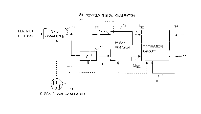
Fig. l is a block diagram shou~ing a configuration of
the quadrature detector of a demodulator according to
this embodiment of the present invention. In the
drawing, like elements and signals are referenced by like
numerals throughout.
In Fig. 1, an A/D converter 10 operates at a high
frequency and directly converts a receivcd analog IF
slgnal into a digltal signal. A fixed clock signal
generator ll generates a clock signal having
approximately four times the frequency of the received IF
signal and actuating t~le A/D converter lO and the
subsequent digital circuits. A delay circuit 12 delays
the output of the A/D converter 10 by one clock time. A
phase rotator 13 performs complex multiplication of the
-
2181843
output signal of the A/D con~erter 10 and the output
signal of the delay circuit 12 by specific values of the
IF frequency to eliminate a phase-rotated component, and
outputs quasi-coherent detected signals. A decimation
circuit 14 receives the quasi-coherent detected signals
which have been output from the phase-rotator 13 at the
frequency of the clock signal of the clock signal
generator 11, and decimates the quasi-coherent detected
signals to output the required quasi-coherent detected
signals for the subsequent step of operation in a
following circuit.
Fig. 2 is a block diagram showing a configuration of
the phase rotator 13 illustrated in Fig. 1.
In Fig. 2, the phase rotator 13 is comprised of an
input terminal 20 for the output signal of the A/D
converter 10, an input terminal 21 for the output signal
of the delay clrcuit 12, an input terminal 22 for a clock
signal which has been output from the clock signal
generator 11, a modulo 4 counter 23 which is actuated by
the clock signal input into the input terminal 22, and
outputs a sequence of (0,1,2,3) outputs repeatedly, a
selector 24 for determining the combination of the input
signals input into the input terminals 20 and 21, based
on the LSB output of the modulo 4 counter 23 and for
outputting the determined two output signals. The phase-
11
-~ 21818~3
rotator 13 is further comprised of an exclusive OR
circuit 25 for the two outputs from the modulo 4 counter
23, a first multiplier 26 for multiplying one of the two
outputs from the selector 24 by the output of the
e~clusive OR circuit 25 to output a quasi-coherent
detected in-phase signal IQc~ a second multiplier 27 for
multiplying the other one of the two output signals of
the selector 24 by the MSB output signal of the modulo 4
counter 23 to output a quasi-coherent detected
quadrature-phase signal QQ~.
In the circult configuration according to this
embodiment of the present invention, the complex signal
generator for generating the complex signals IC- QC and
the phase rotator for obtaining the quasi-coherent
detected in-phase signal IQC and the quadrature-phase
signal QQC are partially combined.
Next, the operation of this embodiment is described.
Now, it is assumed herein that a received signal is
given by Equation (1 ) .
Clocked by a clock signal T which has been output
from the clock signal generator 11, the A/D converter 10
converts the recelved signal into a digital signal. As
described hereinbefore, the frequency of the clock signal
T is set to approximately four times the frequency of the
received IF signal. Now, for the simplified description,
12
-- 2181843
let us assume again the clock signal T ~las exactly four
times the frequency of the recelved IF signal. Then, the
output of the A/D converter 10 is represented by the
following equation:
R(~7~) = A(~lT) COS{~ C~7T 1 C f~ lT)}
= A(~l T~ cos{2~f c~l 14 JC t- ~3 c t ~3 ~n (~IT)}
= A(ilT)cos{Jc~ll2 l-~C 1-~3m(~l7)}
where, fc represents the frequency of tlle received IF
signal, T represents tlle period of the clock signal for
accomplishing A/D conversion and is calculated by t~le
equation T = 1/(4fc), and n represents an integer greater
than zero.
The output signal of the A/D converter lO is divided
into two branched signals, and one of tlle two branched
signals is input into the delay circuit 12. Then, the
output of the delay circuit 12 is given by t~le following
equation:
D(~1~) = A((~l - l)?~cos{~ )/2 t~3c t~ r} (lo)
Now, assuming that the frequency of the received IF
signal i5 sufficiently high, compared wit~l the symbol
rate (this assumption is generally holds true), the
symbol rate, noise components within a predetermined band
having frequencies corresponding to the symbol rate, and
13
~ 2181843
components which fluctuate in a rate including tile
phasing rate beLng equal to or smallcr tilan tile symbol
rate can be neglected and tilc following approximate
equations can be obtained:
I)T)~ T)
", ((11--1) T) = ~ ", (11 T) J ( 1 1,
Consequently, the output signal of the delay circuit
lo 12 approxlmates as shown by tile following EquatLon (12):
D(~1T) ~ ?T) COS{J~ (n --1) / 2 1- ~ c t~ 7T)}
T)cos{Jc~712+~c t-~"~(~7T)-JC12}
~ 1 T) si n {~1 l 2 t- (3 c t ~ )} ( 12)
Consequently, it is found tilat an output signal
D(nT) of the delay circuit 12 approximates a signal whose
phase is ~/2-delayed from that of the output signal R(nT)
of the A/D converter 10 and wilose waveform is a slne
wave .
When expressing tile received sLgnal in terms of
complex numbers wLtil the output signal R(nT) of tile ~/D
converter 10 as the real part and tile output signal D(nT)
of tile delay circuit 12 as tile imaginary part, the
received signal is expressed to be a complex signal
S(nT), phase-rotated (multlplied) by specific values of
tile frequency of the IF frequency fc as follows:
14
~ 2181843
S(/77') -= R(ll7) ~- jD(l~
= ,4 (11 T) COs{~11/ 2 + C 1 ~ ) } + J~ (ll7') 5i n {~111 2 ~ 0 "~ ( r) }
= ,4(nT) e~p[j~Ul l 2 ~- c + (3 m(~1T)}¦ ( 13 )
Consequently, an quasi-collerent detected output can
be obtained by phase-counterrotating (multLplying) t~le
output of the complex signal generator for generating a
complex signal represented by Equation (13), by specific
values of the IF frequency at the subsequent step of
operation.
Thus, t~le complex received IF signal S (nT)
represented by the Equation (13) is input lnto the phase .
rotator 13. In t~le phase rotator 13, by using complex
multiplication, the complex signal S(nT) is phase-
counterrotated (multiplied) by specific values of the IF
f requency
W~len the frequency of the received IF signal is set
to fc~ the complex phase-counterrotating signal C(nT) is
given by the following Equation (14), since the received
IF signal is sampled at four times tile frequency of the
IF frequency at tlle time of A/D conversion.
C(I~T) = exp{-j(2~1JC11T/4JC)}
= exp{ j(~rG 12)} ( 14)
- 2181~43
In t11is case, n is set to be an integer belo~ 4,
being any of a sequenc~ of t~1e integers 0, 1, 2, 3. A
quasi-co~lerent detected output can be obtained by t~e
complex multiplication of S(nT) by C(nT).
BB(.lr) = S(l~l) x C(nT)
T)cxp[j{~17/2t(3c~ ]XexP{-~ 2)}
T)e~cp[j{~3c ~ ]
= ,4(1~T)cos{13c ~ (ltT)~+i~l(nT)sin(~c ~ (~111(~17`)~
= {1(~ jO(~77')}eXP(i~3c)
= IQC(I1T) ~ iQQC(~Z`) ( 15 )
As seen from the above Equation (14), tlle value of
the C(nT) is determined to be any of l, -J, ~ . As
described above, since n is any of a sequence of the
integers 0, l, 2, 3, the modulo 4 counter is set to
output a sequence of t~1e integers 0, l, 2, 3 repeatedly.
mod(ll 14) = O
C(~1T)=~ J mod(~ll4) 2 ~ (16)
J mod(n / 4) = 3 J
Consequently, the output of tl1e pl1ase rotator 13 is
also given by any one of the four equations of Equation
(17).
16
2181843
.
R(~7 ~7~ jD(~7 7 ) mod (/7 l 4) = O
-D(~7T)-~ jR(~l~7~ mod(r1/4) = I
BB(~1T) = < R(~71 _ jD(~77~) mod(l7l4) = 2
D(~7 T) - jR(~77-) mod(~7 / 4) = ~ J
Thus, a quasi-eoherent detected ou~put BB(nT~ ean be
calculated by Equation (17) instead of Equatlon (L5).
Next, referring to Equation (17) and Fig. 2, the
operation of the phase rotator 13 is described.
A cloek signal wilich has been output from the cloek
signal generator 11 is input into the modulo 4 eounter 23
through the input terminal 22. The modulo 4 counter 23
outputs any of a sequence of the integers 0, 1, 2, 3 for
every cloek. When 0, 1, 2, 3 are e;~pressed in binary
notation, they are 00, 01, 10, 11 respeetively. Sinee
the frequeney of the clock signal from the clock signal
generator 11 is set to be four times the fr~queney of tll~
reeeived IF signal, the period of the modulo 4 eounter 23
beeomes equal to t~le period of the reeeived IF signal.
The output signal R(nT) of t~le A/D converter 10 and
the output signal D(nT) of t~le delay circuit 12 are input
into the seleetor 24. The seleetor 24 outputs two kinds
of signals, Ic(nT) and Qc(nT), aeeording to the rule based =
on the LSB output f rom the modulo 4 eounter as shown in
17
-- 2181843
Fig . 2 (b ) .
The exclusive OR circuit 25 Lmplements an exclusive
OR operation for the LSB output and the MSB output of the
modulo 4 counter 23. When the two outputs are equal in
value, the exclusive OR circuit 25 outputs "O". When the
two outputs are diîferent in value, the exclusive OR
circuit 25 outputs "1". The output signal Ic(nT), which
is one of the two output signals from the selector 24,
and the output from the exclusive OR circuit 25 are input
into the first multiplier 26. When the output from the
exclusive OR circuit 25 is "O", the first multiplier 26
outputs the output signal Ic(nT) in its original
polarity. When the output from the exclusive OR circuit
25 is "1", the first multiplier 26 inverts the polarity
of the input and outputs the quasi-coherent in-phase
signal IQc(nT).
Qc(nT), the other one of the two output signals from
the selector 24 and the MSB output i'rom the modulo 4
counter 23 are input into the second multiplier 27. When
the MSB output is "O", the second multiplier 27 outputs
the Qc(nT) in its original polarity. When the MSB output
is "1", the second multiplier 27 outputs the Qc(nT) which
is inverted in its polarity as the quasi-coherent
quadrature-phase signal 4Qc(nT).
Consequently, the quasi-coherent detected in-phase
18
- 2~81843
signal I~c(nT) and the quasl-coherent detected quadrature-
phase signal QQc(nT) from the phase rotator 13 can be
represented by one of the four equations of Equation
(17) .
Since the output signals IQc(nT) and QQc(nT) from the
phase rotator 13 are output at four times the frequency
of the received IF signal, they cannot be used for
baseband demodulation at the subsequent step of
operation. Thus, after the output signals IQc(nT) and
QQc(nT) are input into the decimation circuit 14, they are
clocked by a low-frequency clock signal (normally about
one-fourth of the symbol frequency) input into the input
terminal 9, decimated, and transmitted to the baseband
demodulator .
As described hereinbefore, in this embodiment, the
received IF signal is sampled directly through one A/D
converter, and quadrature detection is accomplis~led by
means of digital signal processing. Consequently, the
accuracy for accomplishing orthogonal detection is high
and the amplitude of the quasi-coherent detected in-phase
signal IQc(nT) and tlle amplitude of the quasi-coherent
detected quadrature-phase signal QQc(nT) can easily become
i dent i cal .
The complex signal generator for obtaining the
output represented by Equation (13) is used so as to
19
2181843
finally obtain the quasi-coherent detected output
represented by Equation (15). The quasi-coherent
detected output can be further represented by any of the
four brief equations of Equation ( 17) . Consequently, by
means of the combination of the complex signal generator
and the phase rotator, other circuit configurations may
be conceived so as to obtain the same output. For
example, in accordance with the theory, polarity
determination of R(nT) and D(nT) may be carried out
first, and IQC and QQC may be selected by the selector 24,
according to Equation (1'7).
Furthermore, the receiving side can conf igure the
demodulation system for signal reception by means of the
demodulator according to the present invention, while the
transmitting side can include a modulation system by
means of an ordinary modulator.
In this embodiment, a hardware co~figuration of the
demodulator according to the present invention is
described. As another aspect of invention, the
demodulation method according to the present invention
may comprise the steps of delaying the received signal
having the carrier frequency by one clock time after A/D
conversion by means of a logical operation, combining the
A/D output with the output which has been delayed by one
clock time so as to obtain the complex signal represented
- 2181843
by Equation (13), and obtaining the quasi-coherent
deteeted output represented by Equation (17) by means of
the complex multlplieation of the above-mentioned complex
signal by the signal given by Equation (16).
Embodiment 2
In this embodiment, a circuit eonfiguration will be
descrlbed which outputs an appropriate quasi-coherent
detected output even if a direct-current offset is
present in the output of the A/D converter, and which
reduces quanti~ation noises occurred at the time of A/D
eonversion .
Fig. 3 is a bloek diagram showing a eonfiguration of
the quadrature detector of a demodulator according to
this embodiment of the present invention.
In Fig. 3(a), a eomplex band pass filter 30
(hereinafter referred to as the complex BPF) eliminates
the direct-current offset component
of the recelved IF signal which has been output
from the A/D eonverter 10 and outputs the two, orthogonal
signals.
Fig. 3(b) shows a eonfiguration of the eomplex BPF.
In Fig. 3(b), the complex BPF is comprised of
an input terminal 31 for the output signal of
the A/D converter 10, an input terminal 32 for a clock
signal which has been output from the cloek signal
21
2l81843
generator 11, a second delay circuit 33 whicll is clocked
by the clock slgnal Lnput into the input terminal 32
to delay the output signal of the A/D converter 10
input into the input terminal 31 by one clock time, a
thlrd delay circuit 34 for further delaying
the output of the second delay circuit 33 by
one clock time, a fourth delay circuit 35 for further
delaying the output of the third delay circuit 34
by one clock time. The complex BPF is further comprised
of a first subtracter 36 for subtracting the output
signal of the third delay circuit 34 from the output
signal of the A/D converter 10 input into the input
termlnal 31, an output terminal 37 for outputting the
output of the subtracter 36 to the phase rotator 13, a
second subtracter 38 for subtracting the output of the
fourth delay circuit 35 from the output of the second
delay circuit 33, and an output terminal 39 for
outputting the output of the second subtracter 38 to the
phase rotator 13.
Next, the operation of the quadrature detector
illustrated in Fig. 3 is described.
Now, it is assumed that the output signal of the A/D
converter 10 is represented by Equation (13) as follows:
22
--- 2181~43
RD(11T) = A(l?/)COS{rj3C~1Tt-~C t-~",(nT)} 1- ADC(IIT)
= A(~7T)cos{23lfc~714.fc t-~3C t-~In(~1r)} t- AD~
= ,4(~7T)cos{7~1/2 t-~c t-~",(11T)} t- ADC(~'T) (18)
In the above Equation (18), ADc(nT) is a direct-
current offset component w~licll is contained in t~le output
signal of tile A/D converter 10. Excepting ADc(nT),
Equation (18) is t~le same as Equation (9).
A received IF signal is input into t~le complex BPF
30 through t~le input terminal 31 and delayed by one clock
time eac~l through the second delay circuit 33, the t~lird
delay circuit 34, and the fourth delay circuit 35
respectively. When tlle output signals of tlle second
delay circuit 33, t~le t~lird delay circuit 34, and t~le
fourth delay circuit 35 are designated R2(nT), R3(nT),
R4(nT) respectively, tlley are repr~sented by the following
equations of Equation (19):
R2(1lT) = A((n - I)T)cos{(n ~ /2 +~3c 1-~m((~l - I)T)} + ADC((/1- I)T)
R3(~1T) = A((~l -2)T)cos~(~l -2)~ l2 +~c +f~",((ll -2)T)} + ADC((11 -2)T)
R4(nT)=A((ll-3)T)cos{(~l-3~l2+~c+~,T,((~-3)T)}+ADC((~ )T (19)
Now, assuming that tile frequency of t~le received IF
signal is sufficiently high, compared with the symbol
rate, the following approximate equations can be
obtained, as in the first embodiment:
23
- 21818~3
A(ilT) ~ ~ 7 - I)T) ~ ? - 2)T) ~ 7 - ~)T)
~",(~ ",((~-I)T)~~",((~1- 2)T)~O",((~ )T ~(20)
ADC(-~T) ~ ADC((ll - I)T) ~ ADC((~1 - 2)~) ~ ADC((~7 ~)T) J
Consequently, R2(nT), R3(nT), and R4(nT) can be
represented by the following approximate equations of
Equation (21):
~2(11T)=A(''~COS{('7-l))-~/2~-~C +~3~n(~lT))+~DC(i1T)
= A(~7T)sin{~z~ /2 t-f3C t-~",(17T)} + ADC(~T)
R3(~ZT)=A(~lT)C05~(~7-2)~/2~-~c- ~~~rn(~lT))~ ADC(~7T) (21
= -A(~?T)COS{~lll /2 +~c ~ ~",(~1T)} + ADC(~
R4 (~?T) = A(n~) cos~ 12 ~- ~ c + ~ "~ (~77`)) + ADC(~Z~)
= -A(~7r)sin{~7~ /2 ~ ~C ~-~3",(~ZT)} + ~DC(~?T)
The first subtraeter 36 subtracts t~le output sLgnal
R3(nT) of the thlrd delay circuit 34 from an input signal
RD(nT) input lnto t~le input terminal 31 and outputs an
output signal Bl(nT). T~le second subtracter 38 subtraets
the output signal R4(nT) of tile fourth delay cireuit 35
from the output signal R~(nT) of t~le seeond delay eireuit
33 and outputs an output signal BQ(nT).
24
~ 2181843
B~ (~1T) = ~D (~77') - R3 (~1T)
=2f~(~1T)cos{~7Jc /2+f~C t r)",(11T)}
BQ(~1T) = R2(~7T) -R4(~T) j, (22)
= 2~(~7T)S;n{~7JC 12 t-~c l ~"~(nT)}
As shown in Equation (22), the outputs of t~le
complex BPF 30 are two, orthogonal signals from which the
direct-current offset component ADc(nT) contained in the
output of the A/D converter 10 is eliminated. Therefore,
the outputs of the complex BPF 30 can be expressed in
terms of complex numbers as follows:
SBP(~7T) = Bl (~?r~ t jBQ(~7T)
= 2 ~ (,7 T) ex p[j {~7~1 / 2 t- ~ ~ t ~ 1 T) ~J~ ( 23 )
Consequently, as in the first embodiment, the quasi-
coherent detected output can be obtained by implementing
the complex multlplication of the above-mentioned output
of the complex BPF 30 by the complex phase-
counterrotating slgnal C(nT) and eliminating the IF
frequency component.
A coefficient 2 of the output of the complex BPF 30
can be eliminated by multiplying 1/2 at the subsequent
step of operation or performing tlle operation similar to
that .
As apparent from Equations (22) and (23), the signal
2181843
component of the output of tlle complex BPF 30 is doubled,
and its electric power is quadrupled. However, the
electric power of the quantization noises contained in
the output of the ~/D converter 10 is only doubled, since
quantization noises are distributed uniformly. Thus, it
can be seen that the effect of the quantization noises
can be reduced equivalently.
As described hereinbefore, in tllis embodiment, two
orthogonal signals are generated through the complex BPF.
Consequently, the direct-current offset contained in the
output of the A/D converter 10 can be eliminated, and the
effect of the quantization noises can also be reduced.
Next, the transfer function of the complex BPF will
be verif ied .
The output side of the complex BPF 30 for outputting
Bl(nT) subtracts a signal which is two-clock time delayed
from an input signal. On the other hand, the output side
of the complex BPF 30 for outputting BQ(nT) subtracts a
signal which is further two-clock time delayed from a
slgnal being one-clock time delayed from an input signal.
Thus, the transfer function H1(z) of the output side of
the complex BPF 30 for outputting Bl(nT) and the transfer
function HQ(z) of tlle output side for outputting BQ(nT)
are represented respectively by tlle following equations
of Equation (24):
26
2181843
hrl (Z) = I _ z -2
HQ(z) = z-l _ z-3 ~ (24)
Consequently, Hl[exp(J~T) ] and E~Q[exp(,J~T) ]
representing t~le frequency characteristics of Hl(z) and
HQ(z) respectively are glven by Equation (25) as follows:
~ (e j~T) = ~ _ e-j2~T
= e i"'T(2jsincl~T)
= 2e-i(~T-~12) sin~T ~ (25)
HQ (e j("T ) = e j("T (I - c 2 j~T )
= e (2jsin~T)
2 -j(2~"T-~/2~ i T
Thus, as is seen from sln~T representing the
amplitude term of EEI[exp (J~T) ] and EEQ[exp (J~T) ], the
frequency characteristics of EEI(z) and HQ(z) indicate the
characteristics of the complex BPF by which the direct
current offset component can be eliminated. Fig. 4 shows
the frequency characteristic of the complex BPF.
Embodiment 3
In tllis embodiment, a complex BPF in accordance ~ith
another embodiment of the present invention is described.
The quadrature detector of a demodulator according
27
21818~3
to the third embodiment of the present invention will be
described, with reference to Fig. 5.
In Fig. 5 (a), reference numeral 40 denotes a second
complex BPF. Fig. 5(b) shows a configuration of the
second complex BPF 40.
In Fig. 5(b), the second complex BPF 40 is comprised
of an input terminal 41 for the output signal of the A/D
converter 10, an input terminal 42 for a clock signal
which has been output from the clock signal generator ll,
a fifth delay circuit 43, a sixth delay circuit 44,
seventh delay circuit 45 which are respectively clocked
by a clock signal input into the input terminal 42 to
delay the input signal of the input terminal 41 by one
clock time each, a third subtracter 46 for subtracting
the output signal of the sixth delay circuit 44 from the
signal input into the input terminal 41, a fourth
subtracter 47 for subtracting the output signal of the
seventh delay circuit 45 from the output signal of the
fifth delay circuit 43, a fifth subtracter 48 for
subtracting the output signal of the fourth subtracter 47
from the output of the third subtracter 46. The second
complex BPF is further comprised of an output terminal 49
for outputting the output of the fift~l subtracter 48 to
the phase-rotator 13, an adder 50 for adding the output
of the third subtracter 46 and the output signal of the
28
2181843
-
fourth subtracter 47, an output terminal S1 for
outputtlng the output of tlle adder 50 to t~le phase-
rotator 13.
Next, the operation of this embodiment will be
described.
When the output signal of tlle A/D convertcr 10 is
represented by Equation (18), output signals R5(nT) of tllc
fifth delay circuit 43, R6(nT) of the sixt71 delay circuit
44, R7(nT) of tl~e seventh delay circuit 45 become
equivalent to R2(nT), R3(nT), R4(nT) given by Equation
(21) respectively. Thus, output signals Bll(nT) of the
third subtracter 46 and BlQ(nT) of the fourtll subtracter
47 are equivalent to Bl(nT) and BQ(nT) given by tlle
equations of Equation (22) respectively.
Consequently, an output signal B21(nT) of t71e fifth
subtracter 48 and an output signal B2Q(nT) of t~le adder 50
are represented by the following equations of Equation
( 26 ) respectively:
B2~ A7~) = B~ BQ (f7~7`)
= 2~/~A(fl .7') COS{77~1 12 1- ~ c t ~ ", (nT) t ~ 14 } ~, 26
B2Q(llT)=B~(f1r-l BQ(f~rf ( )
= 2~f~A(I7~7'~f sln{f7JG / 2 t U C t 13 ~ A7') ~- JC l 4~
Tlle above-mentioned output signals B2l(nT) and B2Q(nT)
are then output from the output terminals 49 and 51,
29
218~843
respectively to the phase rotator 13.
As shown in Equation (26), the output;s of the second
complex BPF 40 are two, orthogonal signals from which the
direct-current offset component is eliminated. Thus,
they can be expressed in terms of complex numbers, and as
in tlle first embodiment, the quasi-coherent detected
output can be obtained, using the complex phase-
counterrotating signal C(nT).
Embodiment 4
In addition to solving the problems presented in the
first embodiment, this embodiment aims to reduce the
effect of the quantization noises which will occur at the
time of A/D con~rersion.
Fig. 6 and Fig. 7 are block diagrams showing a
configuration of the quadrature detector of a demodulator
according to thls embodlment of the present lnvention.
Referring to Fig. 6, a clock signal generator 60
generates a clock slgnal having approximately eight tim~s
the frequency of a received IF slgnal. An A/D converter
61, being clocked by a clock signal which has been output
from the clock signal generator 60, converts the received
IF signal into a digital signal. A two-to-one frequency
divider 62 divides the output frequency of the clock
signal generator 60 by two, an IF signal amplifier 63 is
actuated by the clock signal of the clock signal
-
2181843
generator 60 and by t~l~ clock signal of th~ two-to-one
frequency divider 62 and amplifies the output of the A/D
converter 61.
Fig. 7 shows a configuration of t~le IF signal
amplifier 63. Referring to Fig. 7, an input t~rminal 65
receives the output of t~le A/D converter 61. An input
terminal 66 receives t~le clock signal of t~le clock signal
generator 60. An input terminal 67 receives t~le output
signal of t~le two-to-one frequency dLvider 62. A delay
circuit 68 delays the input signal of the input terminal
65 by one clock time. An adder 69 adds the input signal
of the input terminal 65 and the output signal of the
delay circuit 68. A flip-flop 70 is clocked by the input
signal of the input terminal 67 and latches the output
signal of the adder 69. An output terminal 71 outputs
the output of the flip-flop 70 to the phase rotator 13.
Next, the operation of this embodiLent will be
described .
Now, let us assume t~lat the output signal of the A/D
converter 61 is given by Equation (27).
RE(~1TS) = ~ 7Ts)cos{~cnTs t- (3 c +~ Ts)} (27)
In the above equation, Ts is the period of t~le clock
signal of the clock signal generator 60, and Ts =
1/(8f~F). The output signal of the A/D converter 61 is
31
2181843
input into tlle IE; signal amplif ier 63 . The output signal
of the A/D converter 61 is input into the delay circuit
68 of the IF signal amplifler 63 and delaycd by one clock
time, and in the adder ~9, added to the signal which has
been output from the ~/D converter 61 and input into the
adder 69 WitilOUt passing tllrough the delay circuit 68.
RADD(I1TS) = ~(~7Ts)C0S{(J)c~1Ts t-~7c t-~",(nTs)}
t- ,4((~1 - I)Ts)cos{(J)c(~t - I)Ts t-~c ~n((~7 - I)Ts)}
Ts) COS{~1JI /4 t~3c t ~t~ Ts)}
+ ~ 1T5)COS{JU7/4 t-1~7c t-f3",(~1Ts) -71/4}
= I.8~x ~(~7Ts)cos{ml 14 t~c t~7,~ 1Ts) -~ l8}
(28)
In this embodiment, it is assumed that the same
appro~imate equations of Equation ( 20 ) as described
hereinbefore are also applicable. The sampling frequency
of the output signal of the adder 69 is reduced from
eight times to four times the frequency of tile received
IF signal through the flip-flop 70 and output from the
output terminal 71. Then, as in the first embodiment,
quasi-coherent detection is accomplished.
As apparent from Equation (28), the amplitude of the
output signal of the adder 69 has become about 1. 85 times
that of the output of t~lc A/D convertcr 61, and its power
has become about 3 . 42 times . Thus, the effect of the
quantization noises which occur at the time of A/D
32
2181843
conversion and whose power becomes two tim~s at the time
of A/D conversion can be reduced.
In the present lnvention, the samplLng frequency
does not always have to be eight times the frequency of
the received IF signal. It may be 2n (n is an integer
greater than zero) times the frequency of the received IF
signal, including 16 times, 32 times and the like. The
effect of the quantization noises can be r~duced likewise
by the signal processing method similar to that described
hereinbefore. In this case, a four-to-one frequency
divider for dividing the frequency of the received IF
signal by four should be used instead of the two-to-one
frequency divider 62. The configuration of the IF signal
amplifier 63 does not have to be restricted to the
lS configuration having two taps for implementing the method
of taking moving averages as described in tllis
embodiment. Other configurations such as the one having
four taps for implementing the method of taking moving
averages can also be used.
Embodiment 5
This embodiment shows a configuration combining
features of the second embodiment and the fourth
embodiment. When compared witll the fourth embodiment,
this embodiment aims to further reduce the effect of the
quantization noises at the time of A/D conversion and
33
2181843
also eliminate the direct-current offset component.
Fig. 8 shows a configuration of the quadrature
detector of a demodulator according to the 7. if t~
embodiment of t~le present invention.
Next, the operation of this embodiment is described.
It is assumed herein tllat t~le output signal of t~le
A/D converter 61 is given by Equation (29).
R~ 7Ts) = ~(~1Ts)COS{(J)C~7Ts ~ 7c ~ Ts)} + ~4DC(~1Ts) (29)
The output signal of the A/D converter 61 is input
into the IF signal amplifier 63, and is sub~ect to tlle
same signal processing as in tile fourth embodiment.
Then, the input signal of the flip-flop 70 is calculated
by Equation (30) as follows:
RFr~ Ts) = A(~ITs)cos{~cllTs ~-~C ~ (nTs)} + ~4DC(~?Ts)
t-A((~7 - I)Ts)cos{(J)c(ll - I)Ts ~ ~c ~ ~3"~ I)Ts)l ~ Al~ l - I)rS)
=A(l7Ts)cos{~17ll4+~c+~ 7Ts)}~ ADc(l1Ts)
+A(~ITS) cos{11~ / 4 + (3 C + ~7 ~ Ts) ~ 7l / 4} ~ ADC ~
-I.SsxA(llTs)cos{/l7ll4~c~ lTs)~ }~ D((ll7s) (30)
In the above equation, the approximate equations of
Equation (20) are used, as in the fourth embodiment.
Then, through the flip-flop 70 the sampling frequency is
reduced from eight times to four times the frequency of
the received IF signal.
34
2181843
R~o(2l77Ts) = I~Sx A(2~ 5)COS{2l1lJI /4 ~ ~7c t ~ (2l~l75) ~
~ 2ADC (2rl~ Ts ) ( 3 1 )
When 2Ts = T, Equation (31) becomes equal to
Equation (32). ExceptLng t~lat t~le amplitudc of t~le
signal has become 1. 85 times that of the output signal of
the A/D converter 61, the phase of tlle signal is 1~/8
behind, and that the direct-current offset component llas
become doubled, Equation (32) is t~e same as Equation
(18) .
~rFo("7~ = 18SXA(~77)coS{~7~l2~c +~ 71)-7~18}~ 2ADC("7~ (32)
Consequently, as in t le second embodiment, the
following two outputs can be obtained by performing
signal processing throug~l t~le complex BPF 30:
B~ 7 T) = (2 x l 8 5) x A(~7 T) coslnJc l 2 ~ c + ~ n~ (~7T) ~ ( 33 )
BQQ(17T)=(2xl.SS)xA(nT)sin{~7~l12~c~"~(~7T)~ J
Thus, as in the second embodiment, quasi-coherent
detection becomes possible by using these outputs. As
apparent from Equation (33), the amplitude of the signal
component has become 2 x 1. 85 times that of the output
signal of the A/D converter 61. Consequently, t~le effect
of the quantization noises has been reduced, and the
direct-current offset component has been eliminated.
As described llereinbefore, in this embodiment, the
effect of the quantization noises at the tlme of A/D
21~1843
-
conversion can be reduced by adding and subtracting the
received IF signal sampled at eight times the frequency
of the carrier frequency via the IF signal amplifier 63
and the complex BPF 30. The direct-current offset
component can be also eliminated. As in the fourth
embodiment, the sampling frequency of the signal does not
always have to be eight times. It may be 2n (n is an
integer greater than zero) times t}le frequency of the
received IF signal.
Embodiment 6
An embodiment for improving t~le signal-to-noise
ratio without performing high-speed signal processing is
described .
In the fourth and f if th embodiments, when the
oversampling rate of the received IF signal is high such
as eight times or sixteen times the normal sampling rate,
the sampling frequency must be high, too. Thus, high-
speed signal processing of the circuitry is required.
This embodiment aims to suppress the sampling frequency
by making best use of the aliasing frequency at the time
of the sampling operation, so as to increase the
oversampling rate equivalently without performing high-
speed signal processing.
The configuratlon of t~le quadrature detector of a
demodulator according to this embodiment is the same as
36
2181843
shown in Fig. 6 or Fig. 8. The sampling frequency,
however, is set to satisfy tlle following Equation (35).
Fig. 9 is a diagram showing this relations~lip.
Now, let us assume that the received IF frequency flF
is represented by tlle sampling frequency fS as follows by
Equation ( 34 ):
f~F = M x Js 12 ~ fa (34)
In the above equation, M is an integer greater tllan
zero . Then, the f requency of the output of the A/D
converter 61 is sub,~ect to aliasing in accordance wit~l
the sampling theorem, and becomes equal to fa- When it is
set that f5 = N x f~ (N is a positive integer, equal to or
greater than 2), the output of the A/D converter 61
becomes equivalent to tlle received IF signal whose
frequency has been converted to f~, a difference between
M fS/2 and flF~ sampled at tlle oversampling rate of N.
When the above equation is substituted into
Equation (34), the following Equation (35) is obtained:
Jll; =MXJsl2t JslN
2N f lF = (MN t- 2) JS (35 )
37
- ~ 2181~43
Consequently, the frequency of the output of the A/D
converter 61 sampled at fa becomes equal to fs/N duc to
aliasing. Then, the output after A/D conversion becomes
equivalent to the output for embodiments of the present
invention using sampling at high frequencies. The effect
of the quantization noises thus can be reduced by
implementing the processing operation similar to that
described in the fourth embodiment or the fifth
embodiment .
As described above, in the quadrature detector of
the demodulator according to this embodiment, even if the
sampling frequency is not substantially high, an
oversampling rate can be set to be large equivalently.
Consequently, the effect of the quantization noises can
be reduced in a low-speed signal processing operation.
Embodiment 7
This embodiment provides a demodulator whereby,
regardless of the symbol rate, signal distortion, which
will occur at the time of signal processing, and the
direct-current offset component are eliminated.
Referring to the second embodiment, for example, a
received signal is input into the complex BPF 30 so as to
eliminate the direct-current offset component.
Consequently, the signal is distorted concurrently, as
shown in Fig. 4. This embodiment aims to eliminate this
38
-
~181843
distortion .
Figs. 10 and 11 are block diagrams illustrating a
configuration of the quadrature detector of a demodulator
according to the seventh embodiment of the present
invention.
Referring to Fig. 10, a direct-current offset
eliminator 80 eliminates the direct-current offset
component contained in the output signal of the A/D
converter 10.
Fig. 11 illustrates a configuration of the direct-
current offset eliminator 80.
In Fig. 11, the direct-current offset eliminator 80
is comprised of a four-tapped moving average circuit 100
of the FIR (Finite Impulse Response) type, a subtracter
88 for subtracting the output signal of the four-tapped
moving average circuit 100 from the input signal of an
input terminal 81, an output terminal 89 for outputting
the output of the subtracter 88 to the phase-rotator 13.
The four-tapped moving average circuit 100 is comprised
of the input terminal 81 for receiving the output signal
of the A/D converter 10, an input terminal 82 for
receiving the clock signal of the clock signal
generator 11, delay circuits 83, 84, and 85 clocked by
the clock signal input into the input terminal 82 for
respectively delaying the input signal of the input
39
2181843
terminal 8I by one clocl~ time eac~l, an add~r 8~ for
adding tl~c inpu~ signal of ti~e input terminal 81 and tlle
output signals Or tlle delay circuits 83, 84, and 85, a
four-to-one divider 87 for dividing tile output of tlle
adder 86 by four.
Next, tlle operation of tilis embodiment will b~
described .
Now, let us assume that t~le output signal of ~lle A/D
converter lO is represented by Equation (18).
The outyut sLgnal of tile A/D converter 10 ~s
input into tile direct-current offset ellminator 80
and dLvided into two branched outputs.
One of tlle two branciled outputs is input into
tile moving average circuit 100, wilere the moving average
of thc output is takcn. Wllen assuming an approximation
similar to tllat described in the first embodiment,
the signal component is eliminatcd through
tlle movinF average circuit lOO. Consequently, an outE)ut
RiNtnT) of tlle subtractcr 88 is given by Equation (36).
0
RA~ 7T) = (l l 4)[A(llT)cos{(~)cl?T + ~?c { 13m(l7T)~ + ADC(II7)
+ A((ll - I)T)cos{(~c(l1 - I)Tt ~C t elm((17~ 1)/)} t ADC((~
+ A((fl-2)T)cos{(~)c(-l -2)Tt`~C +13",((1l-2)T)}+ ADC((~2 -2)T)
+ A((.l-3)T)cos{(~c(ll -3)Tt (3C t-~3"~ -3)~)} t ADC((17-3)r)]
=
2181843
(1 14)[A(~71coS{~C117 1 ~)c 1-0",(117)} t ArJ~(111)
t A(llT)sill{~cllTt (`c 1-~",(llr)}~ ADC(IIT
- A(~lr) cos{(llcl?T t (` C 1- ~3", (IIT)} t ''DC(/IT
- A(I1T)si~1{(,)c~7 1-c 1 ~",(lll~} 1- ADC(II7~]
= ADC (ll T) ( 36 )
Then, by subtracting t~le output RM~(nT) of tllc
subtracter 88 given by Equation (36) from t~1e output
signal of tlle A/D converter lO given by Equation (18),
t~le dircct-current offset component can be eliminated.
T1~e output of the subtracter 88 is then output to t11e
phase rotator 13.
As described above, in this embodiment, t~le output
of the A/D converter lO is averaged. Consequently, t~le
direct-current offset component can be eliminated without
processing ttle signal component. T~le sLgnal component
tllus can remain uncilanged, without being distorted, even
if the frequency of t~le received IF signal and t~le symbol
rate are not fully different in value.
T~le configuration of the dlrect-current offset
eliminator 80 does not always have to be the four-tappcd
movLng average circuit. Ot~1er configurations using ot~ler
types of FIR circuits. or an IIR (Infinite Impulse
Response) circuit may also be used.
Embodiment 8
Tllis embodiment provides a demodulator whereby the
41
2181843
signal distortion whic~l ~las occurred i~l the st.ructural
elements is eliminated at t~le subsequent step of
operation so as to enllance accuracy of signal processinF.
In tllis embodiment. when t~le signal component distortion
has occurred in t~le complex BPF 30 of thc quadrature
detector described in the second embodiment, for example,
baseband processing is implemented at the subsequent step
of operation so as to compensate i`or the distortion.
Fig. 12 is a block diagram showing a configuration
of a demodulator according to the eighth embodiment of
the present invention.
Referring to Fig. 12, a distortion compensator 90
compensates for the signal distortion whic~l has occurred
in the complex BPF 30, at baseband.
Next, the operation of t~lis embodiment is described.
Now, it is assumed tllat the signal component has
been distorted t~lrough tlle complex BPF 30, since the
f requency of a recelved IF signal and t~le symbol rate are
not fully different in value. In this case, the signal
distortion is identified by examining t~le transfer
function within the bandwidt~l represented bY Equation
(25). The signal whicil has been distorted through the
complex BPF 30 is still distorted after it has become a
baseband signal or after it has been output from the
decimation circuit 14. Accordingly, when the transfer
42
2181~43
function of tile complex BPF 30 representing i ts frequcncy
charactcristic Ls set to 1{ [ exp ( j~T) ], tilC distorted
signal component can be elimLnated by multiplying by tile
inverse transfer function ~ [exp ( j~T) ] in tile
distortion compensator 90. Consequently, signal
transmission free from distortion becomes possible.
As described above, in this embodiment, tile signal
distortLon wilLch ilas occurred Ln tile complex BPF is
compensated for at baseband. Thus, signal transmission
free from distortion becomes possible even if tile
frequency of the received IF signal and tile symbol rate
are not fully different in value.
In order to eliminate the signal distortion, the
transfer function representing tile characteristic of the
baseband receiving filter and the signal distortion may
also be used and multiplied by its reciprocal. instead of
providing a distortion compensator specifically designed
for that purpose within a demodulator.
In tilis embodiment, a description is directed to the
metilod for compensating for the signal distortion WiliCil
has occurred in the complex BPF 30 having the transfer
function representing its frequency characteristic ~1 [exp
( j~t) ] by means of tile distortion compensator having tlle
inverse transfer function of ii-l [exp (J~t) ] at tile
subsequent step of operation. Thls method is also
43
2~81~43
applicable to compensation for signal distortion which
has occurred in t~le p~lase rotator 13. In t~liS case, the
transfer functions of t~le phase rotator 13 and the
distortion compensator may be set to H2 [ exp ( j~T)
[exp ( j~T) ], respectively.
Embodiment 9
In t~lis embodiment, a description is directed to a
case where an A/D conversion technique by means of
oversampling signals, including delta-modula~ion and
delta-sigma-modulation, being excellent in reducing tilC
quantization noises, is applied to the quadrature
detector portion of a demodulator. In t~lis case, tlle
sampling technique making use of aliasing as described in
the sixth embodiment is applied.
Fig. 13, Fig. 14, and Fig. 16 are block diagrams
respectively showing a configuration of a demodulator
according to the present invention.
In Fig. 13, a clock signal generator 110 generates a
clock signal at a frequency satisfying Equation (35). A
delta-modulator 111 is clocked by the clock signal of the
clock signal generator 110. A frequency divider 112
divides the output frequency of the clock signal
generator 110, and a filter and decimation circuit 113
averages the output of the delta-modulator lll and
outputs the decimated data output.
44
21~1~43
Fig. 14 is a block diagram showing a configuration
of t~le delta-modulator 111. In Fig 14, t~le del~a-
modulator is comprised of an input terminal 120 for a
receiYed I~ signal, an input terminal 121 for the clock
signal of the clock signal generator 110. a sample-and-
hold circuit 122, clocked by the clock signal input into
the input termLnal 121 to sample t~le input signal of the
input termLnal 120, a subtracter 123 for subtracting the
output of an integrator 127 from tile output of the
sample-and-hold circuit 122, a comparator 124 for
detecting tlle polarity of the output of the subtracter
123 and for outputting rl~ when the polarity is positive
and outputting r-1~ whcn the polarity is negative, a
delay circuit 125 for delaying the output of the
comparator 124 by one clock time. a one-bit digital to
analog (hereinafter referred to as D/A) converter 126 for
performing D/A conversion of the output of tile delay
circuit 125, the integrator 127 for integrating the
output of t~le one-bit D/~ converter 126, an adder 128 for
adding the output of the comparator 124 and the output of
a delay circuit 129, tlle delay circuit 129 for delaying
the output of the adder 128 by one clock time, an
~ntegrator 200 comprised of the adder 128 and the delay
circuit 129, an output terminal 130 for outputting the
output of the adder 128 to the filter and decimation
2181843
cLrcuit 113.
Fig. 16 is a block diagram showing a conf iguration
of tlle filter and decimation circuit 113. In Fig. 16,
the f~lter and decimation circuit 113 is comprised of an
input terminal 131 for receiving the output oi` t~le delta-
modulator lll, an input terminal 132 for receiving t~le
output of tlle clock signal generator 110, an input
termlnal 133 for receiving tile output of t~le frequency
divider 112, a moving-average filter circuit 134 which is
clocked by the clock signal of the input terminal 132 to
take the moving average of tlle signal input into tlle
input terminal 131. The moving-average filter circuit - -
134 may be, for example, in the form of the four-tapped
moving-average circuit shown in Fig. 11. The filter and
decim~tion circuit 113 is further comprised of a
decimation circuit 135 which is clocked by a clock signal
input into the input terminal 133 to decimate t~le output
of tlle moving-average filter circuit 134, and an output
terminal 136 for outputting the output of t~le decimation
circuit 135.
Next, t~le operation of a demodulator according to
this embodiment will be described.
It is assumed herein that the output frequencY f5 of
the clock signal generator 110 and the received IF
frequency flF satisfy Equation (35).
46
~ 2181843
In this situation, as in tlle sixt~ embodim~nt, since
the frequency fS/l~ of the output signal of the sampl~-and-
hold circuit 122 becomes fS/N du~ to aliasing, the
frequency fS/E~ becomes equal to t~le frequency of tl~e
received IF signal having a center frequcncy fs~{ sampled
at the oversampling rate of N. Consequently, by delta-
modulating the output of t~le sample-and-hold circuit 122
and integrating the modulated output again via the
integrator 200 wit~lin the delta-modulator, t~le A/D
converted output uslng the lligh-accuracy delta-modulator
is output from the output terminal 130. Furthermore, as
is well known, quantization noises ar~ distributed
uniformly within t~le range of the frequencies up to tile
half of tlle sampling frequency. Fig. 15 shows the
relationship between tlle quantization noise component and
the sampling frequency in the output of the delta-
modulator .
The output signal of the delta-modulator lll output
from the output terminal 130 Ls input into the input
terminal 131 of the filter and decimation circuit 113.
Then, through the moving-average filter circuit 134, bY
eliminatlng the frequency components whlch are higher
than the slgnal frequency, elimination of the
quanti~atlon noise component within the high frequency
band is accomplished. Consequently, the SN ratio is
47
2181843
improved .
The output signal of t~le moving-average filt~r
circuit 134 having aliased oversampling rate, from w~lic~l
the quantization noise component is reduced, is decimated
through tile decimation circuit 135 by tile clock signal
which has been output from t~le frequency divider 112 and
input into the input terminal 133. When the output
frequency of the frequency divider 112 is set to 4 x fS~
it is the same as sampling the received IF signal having
tlle center frequency fs/~ at four times t~le sampling
frequency. Consequently, at the subsequent step of
operation, signal processlng similar to that described
hereinbefore becomes possible, and high-accuracy quasi-
coherent quadrature detection of a digitalized signal
becomes possible.
As described hereinbefore, according to the present
invention, a received IF signal which has been
downconverted by means of aliasing in the sampling
operation is delta-modulated. Consequently, the delta-
modulation technique, whic~l is excellent in reducing the
quantization noises can be applied in low-speed signal
processing .
In the decimation process, as shown in this
embodiment, a low-speed clock signal does not necessarily
have to be generated by dividing the frequency of a high-
48
2181843
speed clock signal. Alt,ernatLvely, anot~er asynchronous
clock signal generator may be used. T~le A/D conversion
technique by means of oversampling signals does not have
to be restricted to the delta-modulation system, eitiler.
A multistage nolse shaping (MASII) system may also be
used .
As described ~lereinbefore, according to the present
invention, a received signal is subJect to ~/D conversion
in the radio frequency range or in the intermediate
frequency range, and quadrature detection is accomplished
by phase-rotating (multiplying) the complex signal by
specific values of the carrier frequency. Consequently,
high-accuracy quadrature detection and high-accuracy
amplitude matching of quasi-coherent detected in-phase
and quadrature-phase signals can be obtained.
Furthermore, the digital BPF is provided in the
quadrature detector. Thus, in addition to t~le above-
mentioned effect of obtaining high accuracy of quadrature
detection and amplitude matc~ling of quasi-coherent
detected in-phase and quadrature-phase signals, tile
direct-current offset component can also be eliminated.
Having t~lUS described several particular embodiments
of the invention, various alterations, modifications, and
improvements ~ill readily occur to t~lOse skilled in the
art. Such alterations, modifications, and improvements
49
~ ~ ~ 1 8 1 843
J
are intended to be part of t~lis disclosure, and are
intended to be within t~le spirit and scope of the
invention. Accordingly, t~le foregolng description is by
way of example only, and not intended to be limitlng.
The invention is limited only as defined in t~le following
claims and equivalents thereto.