Note : Les descriptions sont présentées dans la langue officielle dans laquelle elles ont été soumises.
2 1 83709
ELECTROSTATIC CHUCK MEMBER AND A METHOD Or PRODUCING THE SAME
BACKGROUND OF THE INVENTION
Field of the Invention
This invention relates to electrostatic chuck members
and a method of producing the same. The electrostatic chuck
members are used when a conductive member, semi-conductive
member, insulative m~mh~r or the like is held at adsorption
state by static electricity and particularly incorporated into
a dry etching device, an ion implantation device, a CVD device
or a PVD device used in the production process of large size
integrations or liquid crystals display.
Description of Related Art
Recently, treatments such as dry etching, on
implantation, CVD, PVD and the like constituting a part of a
production process for the large size integrations or liquid
crystals display, e.g. a production device of semiconductors
changes from a wet process into a dry process from viewpoints
of automation and anti-pollution. A greater part of the
treatment through the dry process is usually carried out under
vacuum.
In the dry treatment, it becomes recently important to
improve a positioning accuracy in the formation of pattern on
silicon wafer, glass plate or the like, for example, used as a
substrate from viewpoints of nigh integration of circuits and
fine work.
In order to satisfy such a demand, vacuum chuck or
mechanical chuck has hitherto been adopted in the
transportation, adsorption and fixation of the substrate.
However, since the vacuum chuck is used under vacuum, the
pressure difference is small and the adsorption effect is
less. Even if the substrate can be adsorbed, an adsorbins
~ 1 8370q
portion becomes local and strain is caused in the substrate.
Furthermore, the sas cooling can not be carried out with the
t~mrerature rising in the treatment or the wafer, so that the
vacuum chuck can not be applied to the recent production
process of high-performance semiconductor devices. On the
other hand, the mechanical chuck becomes complicated in the
structure and takes a long time in the maintenance and
inspection thereof.
In o-der to avoid the above drawbacks of the
conventional technique, electrostatic chuck util zing sta'ic
electricity is recently developed and widely adopted.
However, this technique is indic~ted to have the following
problems.
When the substrate is adsorbed and held by such an
electrostatic chuck, charge retains between the subst-ate and
the electrostatic chuck (through the action of adsorption
force) even after the applied vo~tage is stopped, so that the
detaching of the substrate can not be carried out unless the
charge is completely removed.
For this end, it has been attempted to improve the
insulating dielectric material used in the electrostatic
chuck. For example, there are proposed ~ JP-A-6-8089 a
sintered body of a mixture of aluminum nitride powder and
titanium nitride powder or a spray-coated layer thereo~ is
used as a high insulative materia; ~ JP-A-6-302677 titanium
oxide is applied onto the high insulativa material and
aluminum is applied thereto to contact with Si+SiC platei
JP-B-6-36583 -- use of high insulative substance (aluminum
oxide); ~ JP-A-4-304g42, JP-A-5-235152, JP-A-6-8089 use of
aluminum oxide, aluminum nitride, zinc oxide, quartz, boron
nitride, sialon and the likei ~ JP-A-62-94953, JP-A-2-206147,
JP-A-3-147843, JP-A-3-204924 and the like volume resistivity
2 1 8370~
is lowered to improve static electricity by adding TiO2
(titania) having a high dielectric constant to the hign
insulative material in case of further requiring a highe-
static electricity.
~ owever, the conventional Al203TiO2 based (alumina-
titania) spray-coated layer has the following problems tO be
solved.
(1) When Al203 mixed with TiO2 is used as a spray-coated
layer having an electrostatic adsorption performance, the
volume resistivity is small and a slight current flows, so
that it can be expected to improve the static electricity
through Johonson-Larbec effect. However, TiO2 (titania) is a
semiconductive substance, so that the moving rate of
electrical charge is slow and the responsibility (arrival time
or saturated adsorption, adsorption disappearing time ~ when
the application of voltage is stopped is poor. This
responsibility becomes more remarkable under low-temperature
environment.
In order to render the value of volume resistivity
into, for example, a practical state of lxlO9Q-cm, it is
necessary to add 25% by weight of ~itania. In the production
process of semiconductors, the addition of a great amount of
titania means the incorporation of impurity, which brings
about the degradation of quality and results in the
contamination of working environment.
Furthermore, when the temperature of tne semiconductor
wafer to be adsorbed is higher than room temperature, there is
a high possibility that a large leak current is passed to
break wafer circuit because the volume resistivity is too low.
(2) The Al203TiO2 based spray-coated layer is formed by a
spraying process. In the resulting layer, however, the volume
resistivity and adsorption force are largely scattered and
2l 837Gq
also the productivity is low to bring about the rise of _he
cost.
(3) The Al203-TiO2 based spray-coated layer is porcus~ so
that the high surface finishing can not be conducted and the
remaining adhesion of foreign matter is frequently caused.
Furthermore, the adhesion property to the substrate is low, so
that the coated layer is peeled off from the substrate under
service condition, particularly therma7 change.
SUMMARY OF T~E INVENTION
It is an object of the invention to provide an
electrostatic chuck member having a large volume resistivity,
a small scattering thereof and a stable quality.
Tt is anotner object or the invention to provide an
electrostatic chuck member having a strong adsorpticn fo-ce
and an excsllent responsibili.y (-elease property) in the stop
of voltage application.
It is the other object of the invention to ectablish a
t~chnique of advantageously producing the electrostatic chuck
member having the above properties with a high productivity.
The inventors have made various st-dies with respect to
the elec~rostatic chuck member having the aforementioned
problems, particularly the member having an Al203 TiO2 based
spray-coated layer formed on a substrate and have the
following knowledge.
~ The inventors have confirmed from experiments that the
problem in the conventional Al203-TiO2 based spray-coated layer
results mainly from TiO2 (titania). Further, it has been found
that this cause can be overcome when TiO2 iS changed into a
crystal form of TinO2n_1 (n=1-9).
~ It has been found that the follcwing methods are
effective as a technique of surely providing the Al203 TiO2
2183709
based spray-coated layer containing TinO2n1 (n=1-9).
a. Method of spraying an .~1203 TiO2 material under an
atmosphere having a 7 Ow o.~vgen par.ial pressure to isolate
oxygen from TiO~ to change into TinO2n 1 (n=1-9).
Tn this way, TiO2 is changed into Ti~02n 1 (r.=1-9),
whereby the responsibility is improved and the scattering of
the volume resistivity is small and also the qual_ty ar.d
productivity are improved.
b. The spray-coated layer containing TinO~n l ~n=1-9) is
obtained by spraying in an atmosphere containing substantially
no oxygen or ar. air atmosphere capable of cont-ollir.g to a
pressure lower than atmospheric pressure with a plasma
containing hydrogen as a thermal source. In this point, when
the spraying is carried out under a pressure lcwer th~n the
atmospheric pressure, spraying particies flyins in the thermal
source has a strong impact force to the substrate because the
resistance through gas is small, and hence the dense coated
l~yer having a good adhesion force is fonmed. Moreover, the
dense spray-coated layer is posc~ble to be subjected to a high
su-face fir.ishing and also has an effect of decreas ng the
scattering of volume resistivity.
c. When hydrogen gas having a strong reducins action
is used in plasma as a spraying heat source, the change of TiO2
into TinO2n 1 ~n=1-9) rapidly proceeds ar.d the function and
mechanism of the above it~ms a and b can mor~ effectively be
promoted.
The invention is based on the above kncwledge and the
main part and construction thereof are shown below.
~1) An eiectrostatic chuck member comprises a metal
substrate, an undercoat of a metallic spray-coated layer
fo-med thereon and an Al203 TiO2 based spray-coated layer
containing a TinO2n 1 (n=1-9) type compound formed thereon.
21 837û;1
(2) In the electrostatic chuck member, a thickness of the
metallic spray-coated layer is 30-150 um and a thickness of
the A1203TiO2 based spray-coated layer cont~ining the TinO
(n=1-9) type compound is 50-500 ~m.
(3) In the electrostatic chuck member, the Al203TiO2 based
spray-coated layer containing the TinO2~1 (n=1-9) type compound
has a porosity of 0.4-3.~% and a surrace roughness Ra of 0.1-
2 0 l~m
(4) Tha Al203TiO2 based spray-coated layer containing tne
Ti302n1 (n=1-9) type compound is provided at its surface with a
seal-treated layer of an organic or inorganic silicon compound
and has a volume resistivity of lxlO9 - lxlOll Q cm.
(5) The metallic spray-coated layer is a laver made from at
least one starting substance selected from Ni, Al, Cr, Co, Mo
and alloys containing at least one of these metals.
(6) The TinO2n1 ~n=1-S) type compound included ir. the
Al203-TiO2 based spray-coated layer is one or more compounds
selected from the group consisting of Ti30s, Ti203, TiO, Ti407,
TisOg~ Ti601 , Ti801s~ Ti7013 and TigO17.
The above electrostatic chuck member can be produced by
adopting the followir.g methods.
(7) A method of producing an electrostatic chuck m~mh~
comprises subjecting a metal substrate to a blast treatmer.t,
forming an undercoat of a metallic spray-coated layer on a
surface of the substrate, and applying an Al203TiO2 based
ceramic spraying material containing 2-30 wt% of TiO2 thereonto
in Ar gas or air atmosphere adjusted to a pressure of 30-750
hPa through a plasma spraying process containing a hydrogen
gas to form a top spray-coated layer in which a part or whole
of TiO2 in the spraying matarial is changed into a crystalline
compound represented by TinO2n1 (n=1-S).
(8) A method of producing an electrostatic chuck mem~er
21 ~370~j
comprises subjecting a metal substrate to a blast treat~ent,
forming an undercoat of a metallic spray-coated layer on a
surfaca of tha substrate, applying an Al2O3TiO2 based ceram~c
spraying material containing 2-30 wt~ o- TiO2 thereonto in Ar
gas or air atmosphere adjusted to a pressure of 30-750 hPa
through a plasma spraying process containing a hvdrogen gas to
form a top spray-coated layer in wnich a part or whole of TiO2
in the spraying material is changed into a crystalline
compound rapresented by Ti~02~1 (n=1-9) and thereafter finisn-
grinding the top spray-coated layer to a surface rougnnass ~a
of 0.1-2.0 ~m.
(9) A method of producing an electrostatic chuc~ mem~er
comprises subjecting a metal substrate to a blast treatment,
forming an undercoat of a metallic spray-coated laye- on a
surface of the ~ubstrate, applying an A1203TiO2 based ceramic
spraying material containing 2-30 wt% of TiO2 thereonto in Ar
gas or air atmosphere adjusted to a pressure of 30-750 hPa
through a plasma spraying process containing a hydrogen gas to
form 2 top spray-coated layer in which a part o- whole or TiO2
in the spraying material is changed into a crystalline
compound represented by TinO2n_1 (n=1-9) and thereafter finish-
grindins the top spray-coated layer to a surface roughness Ra
of 0.1-2.0 um, and then subjecting the finish ground surface
to a seal traatment with a silicon compound.
(10) The seal treatment is carried out by applying an
organic or inorganic silicon compound to the surface of the
top spray-coated layer and then heating at 120-350C for 1-5
hours.
~RIEF DESCRTPTION OF THE DRAWINGS
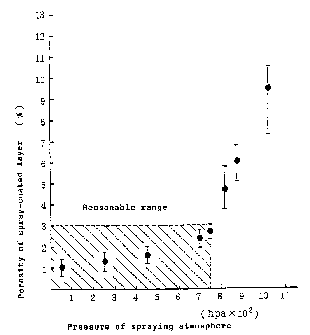
Fig. 1 is a graph showing a relation between atmosphere
pressure in plasma spraying using an Al203TiO2 based ceramic
2l-8370ft
spraying material and porosiLy of the resulting spray-coated
layeri and
Fig. 2 is a diagrammatic outline of an apparatus for
measuring a volume resistivity of an electrostatic chuck
member provided with an Al203 TiO2 based spray-coated layer
formed through plasma spraying process.
DESCRIPTION OF THE PREE'ERR~D EMBODTMENTS
An essential feature of the invention lies in that the
component of the Al203-TiO2 based spray-coated layer formed on
the substrate includes a crystalline compound represented Dy
TinO2n 1 ( n=l-9).
The electrostatic chuck member according to the
invention will be descr~bed in the order or the producti~n
steps together with the method of producins the Al203-TiO2 based
spray-coated layer and its function and mechanism.
(l) Formation of undercoat on metal substrate
In the electrostatic chuck member according to the
invention, Al, Mo, W, C or the like is used as a substrate and
then a surrace of tne metal su~strate is unifonmly roughened
and cleaned by blowing Al203 particles (#60) thereonto.
Then, an undercoat of metallic spray-coated laye-
having a thickness of 30-150 ,um is rormed by spraying a metal
of Ni, Al, Cr, Co, Mo or an alloy thereof as a spraying
material through an arc sprayins process or a plasma sprayins
process.
The action of the metallic spray-coated layer is ba~ed
on the consideration of not only the adhesion force to the
substrate but also the adhesion property to an Al203-TiO2 b~sed
ceramic spray-coated layer subsequently formed as a topcoat.
When the thickness of this layer is less th~n 30 ,um, the
function as the undercoat is low, while when it ~c~c~s 150
2 ~ 8370~;~
~m, the remarkable effect is rot obtained and the formation of
the layer undesirably takes a iong time.
(2) Formation of topcoat
After the fonmation of the metallic spray-coated layer
as the Al203 TiO2 based ceramic spray-coated layer is for~ed
thereonto as a topcoat. The ceramic spray-coated layer will
be described in detail below.
The spray-coated layer obtained by plasma spraying the
commerciaily available Al203-TiO2 based spraying material has
strong peaks of Al203 and TiO~ detected by an X-r~y
diffractometry, from which it is clear that the components of
the spraying material are rendered into coated components as
they are. However, the coated layer consisting of such
crystalline components has problems that the -esponse rate is
slow and the leak current is large as mentioned above.
According tc the invent on, therefore, the same
comm~rcially available Al203 TiO2 based ceramic spraying
material is used and sprayed in an Ar gas atmosphere
containing substantially no air (oxvgen~ or in ar. atmosphere
containing a slight amount of air by using a hydrogen gas
having a strong reducing action as a plasma working gas. In
this case, it has been found that a part of TiO2 releases
oxygen to change into a crystalline compound represented by z
general formula of Ti~02n 1 (n=1-9).
The reason why TiO2 releases oxygen to produce Ti~02~_
(n=1-9) compound when the Al203 TiO2 based ceramic spraying
material is plasma-sprayed using hydrogen gas is considered
due to the fact that Ar, He, H2 or the like is isolated into
ion and electron in the plasma as a spraying heat source to
form a region being electrically neutral as a whole of the
plasma but having locally a high electron density, while TiO2
spraying particles pass through this region to release oxygen
2 1 83709
and change into the form or the TiDO2n-1 (n='-9) compound.
This phenomenon becomes more conspicuous when the
plasma spraying is carried out under a condition that the
spraying atmosphere contains hydrogen but does not contain
oxygen.
According to the inventorsV experiments, Ti30s / Ti20
TiO, Ti407 / TisOs / Ti6011 ~ Ti80ls ~ Ti7013 / TisOl7 and TiloOls are
found as the TinO2n 1 (n=1-9) compound. Among them, Ti30s and
Ti203 are effective.
In the for~nation of the Al203-TiO2 based ceramic spray-
coated layer containing TinO2n 1 ~n=l-9) a~- the topcoat
according to the invention, when the layer is formed in an
atmosphere containing no oxygen under a pressure lower than
atmospheric pressure, resistance of gas to the spraying
particles flying in the heat source reduces, so that the
impact energy of the spraying particles to the substrate
becomes large and the deposition density of the particle~
becomes large accomp~nied therewith and nence the poros~ty of
the coated layer becomes considerably small. It can be said
that this method is suitable.
~ or example, Fig. l shows a relation between porosity
of plasma spray-coated layer obtained by using comm~rcially
available 85 wt% Al203- 15 wt% TiO2 spraying material and
pressure of spraying atmosphera. As seen from this result,
the porosity of the coated layer becomes smaller under a lower
pressure.
Since the topcoat of the spray-coated layer according
to the invention is required to have a porosity of not more
than 3%, the spraying atmosphere pressure satisfying the above
condition is not more than 750 hPa as seen from the above
figure.
Because, the Al203 TiO2 based ceramic spray-ccated layer
2 1 83709
containing Ti~02n 1 (n=1-9) and having a porosity or not more
than 3% develops properties suitable as a coating for the
electrostatic chuck, i.e. the scattering of volume resistivitv
is low, the highly surface finishins is possible and the like.
Particularly, the coated layer hav ng a porosity of more than
3% has drawbacks that the scatte-ing of volume resistivity is
larse to increase the reject ratio, the smoothly polished
finish surface is not obtained ~nd the like.
In the ceramic spray-coated ~ayer accordins tc the
invention, the average surface roughness Ra is required to be
within a range of 0.1-2.0 ~m. Preferably, it is within a
range of 0.1-1.0 ~m. When the finish surface has Ra: less
than 0.1 ~m, the number of polishing steps is uneconomica'ly
large and the residual adsorption force to the wafer is large.
When the surface roughness Ra exceeds 2.0 ~m, the scattering
of volume resistivity becomes large and the inaccuracy of
fixing silicon wafer becomes undesirably large in the use as
the electrostatic chuck.
The amount of TiO2 included in the Al203TiO2 based
ceramic spray-coated layer according to the inventicn is 2-30
wt%, preferably 5-15 wt%. When the TiO2 amount is less than 2
wt%, the value of the volume resistivity of the spray-coated
layer is too high, while when it exceeds 30 wt%, the value of
the volume resistivity is too low and a large leak current
undesirably flows.
Moreover, the thickness of the topcoat is within a
range of 50-500 ~, preferably 100-300 ~m. ~nen the thickness
is less than 50 ~m, the function as the topcoat is not
sufficiently developed and the dielectric strength is
unsuitably low. When it ~c~ s 500 l~m, a long time is taken
in the formation to degrade the productivity and also the
peeling is apt to be caused by tnermal shock.
2 1 8370q
(3) Sealing treatment o_ polished surface
If necessary, an organic silicon compound (comm~rcial~y
available organic si~icone resin) or an inorganic silicon
compound (comm~rcially available silicon alkoxide com~ound) is
applied to the Al203 TiO2 based ceramic sp-ay-coated laver
containing Ti~02n ~ (n=1-9) compound and having a given polished
roughness according to the inver.tion and then heated to 120-
350~ for 1-5 hours.
This procedu-e is to prevent the retaining adhesion of
foreign matter by filling the silicon compound in the rine
porous portions of the spray-coated layer.
In general, the porosity of the Al203 TiO2 based ceramic
spray-coated layer containing TinO2~ 1 (n=1-9) compoun~
according to the invention is as very low as not more than 3%,
so that the sealing treatment is not an essential step.
However, the sealing treatment is said to be preferable
because the sealed surrace prevents tne adhesion of foreign
matter in the industrial use as the electrostatic chuck.
The following examples are given in illustratior. of tne
invention and are not intended as limitations thereof.
Example 1
In this example, the influence of kind of atmosphere
gas and thickness upon the state of formins TinO2~-l (n=1-9) in
tne spray-coated layer is examined ir. the plasma spraying of
Al203 TiO2 based spraying material.
~1) Substrate to be used:
Pure aluminum plate (size: width 50 mm x length 100 mm
x thickness 8 m~)
(2~ Undercoat of spray-coated layer:
Tt is formed at a thickness of 100 ~m by plasma
spraying process of 90 wt%Ni - 10 wt%A1 in air.
(3) Topcoat of spray-coated layer:
2 1 P.370q
It is fonmed on the undercoat at a thickness of 300 ~m
by using A1203 15 wt%TiO2 spraying material through plasmA
spraying process under various pressures and various kinds of
atmosphere.
(4) Spraying abmosphere and pressure:
Ar gas: 30-1000 hPa
~ Air: 30-1000 hPa
(5) Plasma working gas:
A mi x~n gas of Ar and ~2 is used.
(6) r.valuation method:
Each cut section of the spray-coated layers formed
under the above conditions is observed by means of an optical
microscope to measure a porosity, while a part of 'he coated
layer is taken out ar.d placed in an X-ray diffraction device
to measure a change of TiO2 crysta' system.
(7) Test results:
The results are shown in Table 1. As seen from the
results of Table 1, the porosity of the coated layer is within
a range of 0.4-3.0% under conditions of 30-750 hPa in
atmospheres of A- and air and 2 part of TiO2 in 90 wt%Ni - ;0
wt%Al constituting the coated layer changes into Ti305 I Ti2C3
and other TinO2nl type crystal system. Particularly, the peak
of TiO2 disappears substantially completely in P- atmosphere
under 30-200 hPa (Test Nos. 1 and 2), and a great part thereof
changes into TinO2n 1 (n = 1-9) type having a less oxygen
amount.
2 1 83709
Table 1
Spraying
atmosphere Porosity of Results of X-ray diffraction
No. Kind Pres- Remarks
of sure coated layer another
gas (hPa) (%) TiO2 Ti305 Tiz03Tin2 n I
1 30 0.4~ 1.5 not O (o) O
detected Accept-
2 2000.8~ 1.7 not ~ O
detected able
3 Ar 6001.5~ 2.1 ~ O O
4 7502.4~ 3.0 O Co) O O Example
9003.8~ 5.8 0 ~ O O Compar-
ative
6 10007.5~ 10.5 0 ~ O O Example
7 30 0.6~ 1.8 0 ~ O O Accept-
8 2001.0~ 1.7 0 ~ O O able
9 Air 6001.7~ 2.3 0 ~ O O Example
lo 7502.6~ 3.0 0 ~
11 9004.0~ 6.8 ~ Compar-
ative
12 10008.5~ 13.0 ~ Example
(Note) (1) use of Ar/H2 mixed gas as a plasma gas
(2) Ti"02 n- I compound is a compound of n = 4-9.
(3) Symbol in column of X-ray diffraction result as follows:
: strongest diffraction peak, O : strong peak,
: weak peak, - : hardly observed
14
21 8370~
~xample 2
In this ex~mple, a limi~ or finish polishing i`s
measured by using the same coated layer as ~r. ~xzmple 1, while
a thermal shock test is made to measure an adhesion property
of the coated layer and a mechanical resistance through
thermal shock.
(1) Substrate to be used: same as in Example 1
(2~ Undercoat of spray-coated layer: same as in Example 1
(3) Topcoat of spray-coated layer: same as in Example 1
(4) Spray ng atmosphere and pressure:
Ar gas: 60, 200, 750, 900, 1000 hPa
(5) Plasma wo-king gas: same a~ in Example 1
(6) Evaluation method:
The coated layer prepared by the above procedure is
polished to render into a mirror surface as far as possible,
which is heated in air at 300~ for 10 minutes and cooled in
air to room t~mperatu-e and this procedu-e is repeated 10
times to measure a chanse of appearance of the coated layer
(average roughness Ra).
Moreover, this test is conducted with respect to the
coated layer in which a silicon alkoxyde compound is applied
three times and subjectad to a drying tr~atment at 200~ for 30
minutes to measure the effect.
(7) Test results:
The results are shown in Table ~. As seen from Table
2, the coated layer formed by spraying under a low p~essure
(60-750 hPa) is small in the porosi.y ar.d smooth in the finish
polished surface. However, when the spraying pressure is 900
hPa or 1000 hPa, the smooth polished surface is not obtained.
~ecause, it is considered that the coated layer formed under a
low pressure (30-750 hPa) has a polished surface having Ra:
O.1-2.5 ~ owing to the low porosity, while in the coated
21 '~3709
layer having a hish porosity (900-1000 hPa), the porous
portion is exposed in form or pit and hence the surface
roughness is necessarily large.
On the other hand, the thermal shock resistances of
these coated layers develop relatively good properiies ur.der
this test conditions independently of the presence or absence
of the sealing agent. Only in the coated layers (Nos. 4 and
5) containing no sealing agent, the occurrence of slight
cracking is observed after the repetition of the tast 8 times.
From the above results, it has been confirmed that the
smooth polishing is possible because tne coated laye-
according to the invention is dense, and tne resistance to
thermal shock is good under the conditions in this example
irrespectively of the sealing agent.
16
21 8370~1
Table 2
Spraying Properties
atmosphere coated layer Sealing Results of
thermal Remarks
No. Pressure Porosity Surface shock test
roughness treatment
(hpa) (~) Ra (~m)
1 60 0.5~ 1.5 0.1~ 0.3 no cracking Acceptable
2 200 0.8~ 1.7 0.3~ 0.5 after 10
3 750 2.4~ 3.0 0.8~ 2.5 absence times Example
4 900 3.8~ 5.8 3.2~ 3.5 Occurrence
of slight Comparative
1000 7.5~ 10.5 3.2~ 4.1 cracking at Example
8 times
6 60 0.5~ 1.5 0.1~ 0.3 Acceptable
7 200 0.8~ 1.7 0.3~ 0.5 no cracking Example
8 750 2.4~ 3.0 0.8~ 2.5 presence after 10
9 900 3.8~ 5.8 3.2~ 3.5 times Comparative
1000 7.5~ 10.5 3.2~ 4.1 Example
(Note) (1) Ar/H2 mixed gas is used as a plasma gas.
(2) Crystal type of coated layer is the same as in Table 1.
(3) Conditions of thermal shock test are 10 times repetition of
300~ x 15 minutes = room temperature.
2~8~o9
Example 3
A volume resistivity of the Al2C3TiO2 based ceramic
spray-coated layer according to the invention is measured, and
the scattering thereof is comr~red with that obtained by the
conventional spraying process.
~1) Substrate to be used: same as in Example '
(2) Undercoat of spray-coated layer: same as in Exa~ple 1
(3~ Topcoat of spray-coated layer:
It is formed at a thic~ness o.~ 250 ~m or 50C ~m by
using Al2Os - 14 wt%TiO2 material through plasma sp-aying
process under various pressures and various gas atmospheres.
(4) Spraying atmosphere and pressure:
Ar gas: 60, 750, 1000 hPa
~ Air: 60, 750, 1000 hPa
(5) Plasmz working gas: use of Ar/~2 mixed sas
(6) Evaluation method:
A dotite (Ag paste) is applied onto the surface of the
spray-coated layer as an electrode and a direct current of
500V is applied between the dotite and the aluminum substrzte
to measure a resistivi~y, from which a volume resistivity is
calculated according to the rollowing equation.
Volume resistivity p = RA/d ~Q-cm~
A: electrode area (c~2) d: cGa~ed layer thickness (cm~ R:
resistivity (Q)
The measurement is 5 positions every one coated layer,
and also the effect of sealing treatment with a silicon
alkoxvde compound (200~ x 30 minutes drying after the
application, 3 times repeat) is examined.
(7) Test results:
The results are shown in Table 3. As seen from the
results of Table 3, the ~omr~rative ~pray-coated layers (Nos.
5, 6, 11, 12) formed under air or Ar spraying atmosphere of
18
2 1 83709
1000 hPa are large in the scattering of volume resistivity and
the effect of the sealing treatment is not clear.
~ n the coated layers accoraing to the inventior. (Nos.
1-4, 7-10), the porosity is small and the property is dense
and a part of TiO~ in the spraying material changes into TinO2
(n = 1-9), so that the scattering of the measured value is
less and the value of volume resistivity required ir. the
electrostatic chuck according to the invention is within a
range of lxlO9-10ll Q-cm and it is conrirmed that the quality
control is very easy.
19
Table 3
Spraying Properties of spray-coated layer Volume Remark
atmosphere resis-
No. Kind Pres- thick- Porosity Ti~ reality ~ivity
of sure ness 21~ I treatment
gas (~IPa) (~m) (%) (Q ~cm~)
1 60 250 0.5~ l.S presence presence Ix10~~ 10~
2 60 SOO 0.5~ 1.4 presence absence lx10~~ 10~ Acceptable
3 Ar750 250 2.4~ 3.0 presence presence lx 109 ~ 10l I Example
4 750 500 2.2~ 2.8 presence absence lx109 ~ 10"
5 10()0 250 7.5~ 10.5 absence presence lx 107 ~ 10l 3 Comparative
6 1000 500 7.2~ 10.fl absence absence lx1()7 ~ 10~ Example
7 60 250 0.5~ 1.6 presence presence lx 101 ~ 101 I r~
8 60 500 0.5~ 1.5 presence absence Ix10~ n~ 101 1 Acceptable C~
9 Air 75() 250 2.3~ 3.0 presellce presence lx109 ~ 10~ Example ~_!
750 500 2.4~ 3.0 presence absence lx 109 ~ 1011
11 1000 250 7.8--11.5 absence presence lx1()7 ~ 1013 Comparative
12 1000 500 7.9~ 12.0 absence absence lxlO~ ~ 10~ 2 Example
(Note) (1) Ti305, Ti203 and other TinO2n-1 (n=4-9) are included in TinO2n-1.
(2) The sealing treatment is a treatment that drying of 200''cx3()
minutes is repeated 3 times after the application of silicon alkoxyde compound.
~l 837ûq
Example 4
Tne adsorpticn force to silicon wafer and ~he decaying
rate or residual adsorption force are measured in the
electrostatic chuck provided with the Al203TiO2 based ceramic
spray-coated layer according to the invention.
(1) Electrostatic chuck substr~te:
A disc-like aluminum alloy having a thickness of 40 mm
and a diameter of 200 mm is used as a substrate and blasted
with alumina, and an undercoat of 50 wt%Ni - 10 wt%Al is
formed thereon at a thickness of 100 ~m through plasma
spraying process in air. Thereafter, Pl2O3 8 wt~TiO2 spray-
coated layer is formed on the undercoat at a thickness of 300
~m in the same manner as in Example 1. Then,
polymetnylsiloxane polymer is appl-ed and subjec~ed to a
sealing treatment at 250C for 1 hour.
Moreover, A~2O3 8 wt%TiO2 is rormed at a thickness of
300 ~m in air as a comp~rative example.
(2) Evaluation method:
Fig. 2 shows an outline or an apparatus of measuring
the adsorption force to silicon wafer and the decaying rate of
residual adsorption force in the spray-coated layer according
to the invention. This apparatus comprised a vacuum vessel 1,
a spray-coated layer 3 fixed to a central portion of the
vessel through an electrostatic chuck substrate 2 of aluminum
alloy, and a silicon wafer 4 statically placed on the spray-
coated layer 3. Further, the electrostatic chuck substrate 2
is provided with a hole ~ flowing a refrigerant for cooling
and connected to a power source 6 located outside the vacuum
vessel 1. Moreover, a ground line 7 is attached to the
silicon wafer, while an insulative ceramics 8 is arransed on
an upper half portion of the electrostatic chuck.
(3) Test results:
2 1 83 70q
The electrostatic adsorption force to sili-on wafer in
the application of voltage and the decaying sta~e of residual
adsorption force after the stop of vo~tage application are
shown in Table 4.
As seen from the results of Table 4, the adsorption
force of the comp~rative spray-coated layer 24-3C gf/c~2 at an
applied voltage of 250V and 30-i50 gf/cm2 at an applied
voltage, while the spray-coated laye_ accordins to tr.e
invention exhibits adsorption forces Oc about 100 gf/cm2 at the
former voltage and 300-350 gf/cm2 at the latter vcltase,
respectively.
As to the decaying rate of adsorption force, the
residence of 3-10 sf/cm2 is obse-ved in the sprav-coated layer
of the comr~rative example even after the 60 seconds of
voltage cut, while the adsorption force complete y disappears
within 1 second after the voltage cu~ in the spray-coated
layer according to the invention.
Table 4
Spraying Electrostatic Kesidual
atmosphere Ti" Sealing absorption force absorpton
No. Kind Pres- (gf/cm~) force(gf/cm~) Remarks
of sure 2 n l treatment after after
gas (hPa) 250 V 500 V second seconds
1 60 presence presence 95~ 103 300~ 350 0
2 Ar 60 presence absence 98~ 105305~ 345 0
3 750 presence presence 95~ 102300~ 348 0 - Acceptable
4 750 presence absence97~ 1()63n4~ 350 0
presence presence 96~ 102302~ 345 n
6 Air60 presence absence 95~ lol305~ 335 0 - Example
7 750 presence presence 90~ 100310~ 330 0
8 750 presence absence 92-~100302~ 331 0 - ~Jl
9 Air1005 absence presence 5~ 8 25~ 30 5~ 23 3~ 10 Comparative O
1005 absence absence5~ 7 24~ 28 4~ 24 4~ 8 Example
Note) (1) Titanium oxides capable of being represented by Ti305, Ti~03 and
other TinO2n 1 (n=4-9) are included in TinO2n ,
(2) The sealing treatment is a heating of 200cx30 minutes after the
application of polymethylsiloxane polymer.
21 8370i~
Example 5
In this example, the adhesion property of the .~1203-TiO2
based ceramic spray-coated layer according to the invention is
examined in the presence or absence of the unde-coat of the
spray-coated layer.
(1) Substrate to be used:
A comm~rcially available material of Al, Mo o- W is cut
into a substrate of width 50 mm x length 100 mm x thickness 8
~m.
(2) Undercoat:
Tt is fo-med on the substrate at a thickness of 3G, 100
or 150 ~m by using the same spraying material as in Example 1
through plasma spraving process in air.
(3) Topcoat:
It is formed at a thickness of 300 ~m by using the same
spraying material as in Example 1 and a mixed plasma frame of
hydrogen gas and Ar gas in Ar of 60 hPa.
Moreover, the topcoat is directly formed on the
substrate without the formation of ths undercoat as a
comr~rative example.
(4) Evaluation method:
After the test specimen of the above coated layer is
heated in air at 300C for 10 minutes and cooled bv blowing air
of room temperature, this procedure is repeated 10 times to
measure the presence or absence of cracking and peeling in the
topcoat of the spray-coated layer.
(5) Test results:
The results are shown in Table 5. As seen from Table
5, the occurrence of cracking is caused in the topcoats having
no undercoat (Nos. 10, 11, 12~ by repeating thenmal shock test
2-3 times irrespectively of the kind of the substrate
material, and also 30-50% of the coated layer is peeled of L.
24
2 1 83709
On the contrary, the topcoats having the undercoat
according to the invention (Nos. 1-9) exhibit good adhesion
property irrespectively of the kind of the substrate material
and have no problem even after the repetition of thermal shock
test 10 times.
Table 5
No. Substrate Thickness of Thickness oF Result of thermal Remarks
material undercoat(~m) topcoat(~m) shock test
1 30 300
2 Al 100 300
3 150 300 Accept-
4 30 300 no cracking
Mo 100 300 able
6 150 300 after 10 times
7 30 300 Example
8 W 100 300
9 150 300
Al none 300 peeling at 2 times Compar-
11 Mo none 300 peeling at 3 times ative
12 W none 30 peeling at 3 times Example
(Note) (1) A spraying material for the undercoat is 90 wt~Ni-10 wt%Al.
(2) A spraying material for the topcoat is Al203-15 wt~TiO2
2 1 8370(~
As seen from the above, the ceramic spray-coated layer in
which a part or whole of TiO~ coexisting with A1203 ' S changed
into a crystalline compound represented by a general fo-mula
of TinO23 1 (n = l-S) according to the invention is st-ong in
the adsorption force to silicon wafer or the like, fast in the
decayins rate of residual adsorption force and is very
excellent in the basic properties as an electrostatic chuck.
Furthermore, the adhesion properties cf the undercoat to ~he
substrate and the tcpcoat to the undercoat and the denseness
are excellent and the quality is stable.
Moreover, the scattering of volum.e resistivitv i~
small, so that the quality contrcl is easy and the
productivity is high. Therefore, the invention largely
contributes to the development of incustrial rields using the
electrostatic chuck.
26