Note : Les descriptions sont présentées dans la langue officielle dans laquelle elles ont été soumises.
CA 02184321 2004-05-05
LAMP STARTIP1G CIRCUIT
Field of the Invention:
The present invention relates to an improved circuit
for starting, operating and hot restarting a high pressure
sodium (HPS) lamp or other high intensity discharge lamp
using a voltage multiplying circuit which is automatically
disabled if the lamp fails to ignite within a predetermined
interval.
21 J~~321
- 2 -
Background of the Invention:
As is well known in the art, high pressure sodium
(HPS) lamps are difficult to start and require special
circuitry for restarting if the lamp is extinguished after
sufficient operation to elevate its temperature. This is
normally known as hot restarting and is known to require
high voltage and energy across the lamp, considerably
higher than can be provided by the line operating voltage.
In commonly-assigned U.S. Patent Nos. 5,047,694 and
5,321,338, various hot restarting circuits for HPS and
other high intensity discharge lamps are described. These
circuits include a storage capacitor and an SCR connected
across a tapped portion of a ballast with a breakdown
device to start the SCR. A charging circuit for the
storage capacitor includes a diode, a pumping capacitor and
a choke connected in series from the ballast tap to the AC
line, and a further diode interconnecting the capacitors.
The pumping capacitor increases the charge on the storage
capacitor in a stepwise fashion until the breakdown voltage
is reached, whereupon energy in the form of high voltage
starting pulses is applied to the lamp.
In cases where a high intensity discharge lamp is
defective or is otherwise incapable of starting, it is
desirable to automatically disable the starting circuit
after a certain period of time in order to prevent damage
to the dielectric components of the circuit from repeated
high voltage pulses. The aforementioned U.S. Patent Nos.
5,047,694 and 5,321,338 disclose two ways in which this may
be accomplished. In one embodiment, a thermostatic switch
is connected in series between the pumping capacitor and
storage capacitor and is opened by an associated heating
resistor after a certain period of time (approximately 3 to
minutes) to terminate the stepwise charging of the
storage capacitor. Although this is an effective
i
CA 02184321 2004-05-05
arrangement, it has the disadvantage'that the disablement
time will depend to some extent on the ambient temperature
at the luminaire, which can range from °30° C for an
outdoor installation to more than +90° C when the HPS lamp
is operating= In a second embodiment, which does not have
this disadvantage, the disabling circuit is electronic in
operation rather than thermal. In this embodiment, a
capacitor having a value much larger than that of the
storage capacitor is used to slowly accumulate a charge
that opposes the charge on the storage capacitor,
eventually preventing the storage capacitor from attaining
the necessary breakdown voltage. In the specific
embodiment disclosed, the high voltage starting pulses are
generated every 0.45 second and are terminated by the
disabling circuit after 4 pulses have occurred. Despite
its temperature insensitivity, however, the capacitive
disabling circuit is disadvantageous in that it requires a
high value capacitor (on the order of 100 microfarads)
which is not only expensive, but is physically large and
difficult to fit onto the same circuit board with other HPS
starting components.
Summary of the Inventions
Accordingly, the present invention seeks to
provide a hot restarting circuit for a high intensity
discharge lamp which, in the case of a failed lamp, is
automatically disabled after a predetermined interval that
is accurately predictable and substantially independent of
temperature.
A further aspect of the invention seeks to provide a
hot restarting circuit for a high intensity discharge lamp
which is relatively simple in contructioa, and does not
require the use of expensive or physically large components.
I !',
CA 02184321 2004-05-05
- 4 -
The foregoing aspects are substantially achieved by
providing an apparatus for starting and operating a high
intensity discharge lamp which comprises, in combination,
a pair of input terminals for supplying voltage to the
apparatus, a~pair of output terminals for connection to a
high intensity discharge lamp, a step-up transformer for
coupling the input terminals to the output terminals, and
a voltage multiplier circuit coupled to a primary winding
of the transformer. The voltage multiplier circuit
comprises a device for blocking high-frequency current, a
first capacitor and a first rectifier element connected in
a first series circuit with the device for blocking high-
frequency current to the primary winding, a second
capacitor and a second rectifier element connected in a
second series circuit with the device for blocking high-
frequency current to the primary winding, and a voltage
response switching device connected in a closed-loop series
circuit with the second capacitor and the primary winding.
When the second capacitor is charged to the breakdown
voltage of the switching device, the switching device
becomes conductive to provide a discharge path for the
second capacitor through the primary winding, thereby
inducing in the secondary winding of the transformer a high
voltage pulse for igniting a discharge lamp connected to
the output terminals. The voltage multiplier circuit also
includes an inhibiting circuit for inhibiting the action of
the second capacitor and starting of the lamp after a
predetermined interval if the lamp has not ignited. The
inhibiting circuit comprises a positive temperature
coefficient resistor connected in series with at least one
of the first and second series circuits, and may also
include a third rectifier element connected between the
positive temperature coefficient resistor and the primary
winding for conducting a heating current through the
21~~321
- 5 -
positive temperature coefficient resistor during alternate
half-cycles of the supply voltage.
In accordance with another aspect of the present
invention, an apparatus for starting and operating a high
intensity discharge lamp comprises, in combination, a pair
of input terminals for supplying voltage to the apparatus,
a pair of output terminals for connection to a high
intensity discharge lamp, a step-up transformer for
coupling the input terminals to the output terminals, and
a voltage multiplier circuit coupled to a primary winding
of the transformer. The voltage multiplier circuit
comprises a device for blocking high-frequency current, a
first capacitor and a first rectifier element connected in
a first series circuit with the device for blocking high-
frequency current to the primary winding, a second
capacitor and a second rectifier element connected in a
second series circuit with the device for blocking high-
frequency current to the primary winding, and a voltage
response switching device connected in a closed-loop series
circuit with the second capacitor and the primary winding.
When the second capacitor is charged to the breakdown
voltage of the switching device, the switching device
becomes conductive to provide a discharge path for the
second capacitor through the primary winding, thereby
inducing in the secondary winding of the transformer a high
voltage pulse for igniting a discharge lamp connected to
the output terminals. The voltage multiplier circuit also
includes an inhibiting circuit for inhibiting the action of
the second capacitor and starting of the lamp after a
predetermined interval if the lamp has not ignited. The
inhibiting circuit comprises a controlled switching device
which is connected across the second capacitor for
discharging the second capacitor when a predetermined
voltage is applied to a control terminal of the switching
21 ~;~~321
- 6 -
device, and a third capacitor connected to the control
terminal for applying the predetermined voltage to the
control terminal. Preferably, the third capacitor is
connected to the second capacitor so as to be charged by
the second capacitor.
In accordance with another aspect of the present
invention, a method for starting and operating a high
intensity discharge lamp comprises the steps of receiving
an input AC voltage waveform from an AC source; during a
first polarity half-cycle of the input AC voltage waveform,
charging a first capacitance through a first rectifier
element; during a second polarity half-cycle of the input
AC voltage waveform, charging a second capacitance through
a second rectifier element and transferring charge from
the first capacitance to the second capacitance; repeating
the preceding method steps to stepwise charge the second
capacitance until the second capacitance reaches a
predetermined potential in excess of the peak magnitude of
the input AC voltage waveform; upon the second capacitance
reaching the predetermined potential, discharging the
second capacitance through a primary winding of a step-up
transformer to induce a high voltage pulse in a secondary
winding of the transformer; coupling the high voltage pulse
to a high intensity discharge lamp to ignite the lamp;
repeating the preceding method steps to generate and couple
a plurality of successive high voltage pulses to the high
intensity discharge lamp; establishing a predetermined time
interval by causing current to flow through a temperature
dependent resistance; and terminating the generation and
coupling of high voltage pulses to the high intensity
discharge lamp after the predetermined time interval has
expired. Preferably, the temperature dependent resistance
comprises a positive temperature coefficient resistance
21~~321
through which at least one of the first and second
capacitances is charged.
In accordance with a still further aspect of the
present invention, a method for starting and operating a
high intensity discharge lamp comprises the steps of
receiving an input AC voltage waveform from an AC source;
during a first polarity half-cycle of the input AC voltage
waveform, charging a first capacitance through a first
rectifier element; during a second polarity half-cycle of
the input AC voltage waveform, charging a second
capacitance through a second rectifier element and
transferring charge from the first capacitance to the
second capacitance; repeating the preceding method steps to
stepwise charge the second capacitance until the second
capacitance reaches a predetermined potential in excess of
the peak magnitude of the input AC voltage waveform; upon
the second capacitance reaching the predetermined
potential, discharging the second capacitance through a
primary winding of a step-up transformer to induce a high
voltage pulse in a secondary winding of the transformer;
coupling the high voltage pulse to a high intensity
discharge lamp to ignite the lamp; repeating the preceding
method steps to generate and couple a plurality of
successive high voltage pulses to the high intensity
discharge lamp; establishing a predetermined time interval
by causing current to flow into a third capacitance through
a resistance until a predetermined control voltage is
reached; coupling the control voltage to the control input
of a controlled switching device to place the controlled
switching device into conduction; and terminating the
generation and coupling of high voltage pulses to the high
intensity discharge lamp after the predetermined time
interval has expired by discharging at least one of the
21 ~~321
_ 8 _
first and second capacitances through the controlled
switching device.
Brief Description of the Drawings:
Referring now to the drawings, which form a part of
the original disclosure:
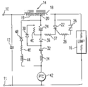
Figure 1 is a schematic diagram of a hot restarting
circuit in accordance with a- first embodiment of the
present invention; and
Figure 2 is a schematic diagram of a hot restarting
circuit in accordance with a second embodiment of the
present invention.
Detailed Description of the Preferred Embodiments:
In the circuit shown in Figure 1, terminals 10 and 11
are provided so as to be connectable to a suitable AC
source which would typically be 240-volt RMS line voltage.
A power factor correcting capacitor 12 is connected between
terminals 10 and 11 in a conventional manner. An inductive
ballast indicated generally at 14 has one end terminal
connected to terminal 10 and the other end terminal
connected to one terminal of a high pressure sodium (BPS)
lamp 16, the other side of lamp 16 being connected to
terminal 11. Thus, the ballast 14 and lamp 16 are in
series circuit relationship with each other across the AC
source terminals 10 and 11.
Ballast 14 is a tapped ballast such that it has a
first winding portion 18 and a second winding portion 19
which are inductively coupled, portion 1H constituting a
much smaller number of windings than portion 19, preferably
on the order of about 5% of the total number of windings of
the ballast. A tap 20 is provided at the junction between
winding portions 18 and 19.
~1~~~2~
_ g _
A semiconductor switch 22 such as a silicon-controlled
rectifier (SCR) or the like is connected so that one end of
its switchable conductive path is connected to the end the
of first portion 18 of the ballast and a high energy
storage capacitor 24 has one end connected to tap 20. The
other end of the capacitor is connected to the other end of
the conductive path of SCR 22. A sidac 26 or other break-
down device is connected between the gate and anode of the
SCR 22, a current-limiting resistor 28 being included in
series with the sidac 26 if the characteristics thereof
require current limitation.
As will be recognized from the circuit thus far de-
scribed, the SCR 22, capacitor 24 and sidac 26 are
connected such that if the voltage on capacitor 24 is
increased to a level such that it reaches or exceeds the
threshold voltage of the breakdown device, the sidac 26
will become conductive, placing the SCR 22 in a conductive
state and discharging the capacitor 24 through winding
portion 18. Because the windings are inductively coupled,
portion 18 acts as the primary of a transformer, inducing
a voltage in the significantly larger winding portion 19,
and generating a high voltage therein which is then imposed
upon lamp 16. As is well understood from a circuit of this
type, proper selection of winding relationship creates a
voltage which is sufficiently high to ignite the lamp 16.
A charging circuit for capacitor 24 is connected be-
tween tap 20 and terminal 11 at the other side of the AC
source. This charging circuit includes a first diode 30,
a pumping capacitor 32 and a radio frequency choke 34,
these components being connected in series between tap 20
and terminal 11. A second diode 36 is connected between
capacitor 24 and capacitor 32 and is poled in the opposite
direction from diode 30.
218431
- 10 -
The circuit including SCR 22, sidac 26, capacitors 24
and 32, diodes 30 and 36, and RF choke 34 will be referred
to as the starter circuit. The operation of starter cir-
cuit is as follows.
During one half-cycle of the AC supply, a current
flows through choke 34, capacitor 32 and diode 30 to charge
capacitor 32. This capacitor is chosen to be relatively
small, significantly smaller than capacitor 24, typically
having a value of about 0.068 microfarads. On the next
half-cycle, capacitor 24 is charged and the voltage across
capacitor 32 aids the incoming source half-wave so as to
deliver energy on the order of 3.9 millijoules to storage
capacitor 24. Capacitor 24, which can be on the order of
microfarads, obviously requires more energy than can be
supplied by the incoming source and capacitor 32 in one
cycle. Accordingly, on the next half-cycle, capacitor 32
is again charged and again delivers energy to capacitor 24
on the subsequent half-cycle, each subsequent cycle
increasing the charge on capacitor 24 in a kind of voltage
multiplying or pumping action. With capacitors of the
value indicated, approximately 25 cycles are required to
charge capacitor 24 to a level of 520 volts, which is a
suitable breakdown level for sidac 26.
When the voltage on capacitor 24 reaches the sidac
breakdown voltage, the sidac 26 becomes conductive,
rendering the SCR conductive and discharging capacitor 24
through winding portion 18, generating the high voltage in
winding portion 19. The large-magnitude capacitor 24
releases considerable energy into the magnetic field of the
reactor 14 (e. g., 0.676 joules as compared with 0.00063
joules in a more conventional HPS starter), which excites
the core of the reactor to a relatively high degree. The
highly excited reactor 14 with its corresponding collapsing
magnetic field pushes the lamp into complete discharge and
~ 1 ~~~r32
- 11 -
into a low impedance state so that the discharge can then
be picked up and maintained by the normal AC source. The
discharging capacitor 24 produces current flow which is in
the same direction as the continued current flow produced
by the collapsing field and is forced through the lamp 16
as the SCR 22 is turned off by the instantaneous back
voltage bias placed on capacitor 24 by the same collapsing
field energy.
In this controlled step-charging of the large energy
storage capacitor 24, there is no need for a high wattage,
low magnitude series-connected resistor which would produce
high-wattage loss. Thus, the circuit is very efficient and
does not generate heat.
A 10 ohm wire-wound resistor 37 can be connected in
series with SCR 22 to cause the peak of the high-voltage
pulse to be lower and the base (width) of the pulse to be
longer. This decreases the dielectric stress which allows
use of lower cost magnetic components. This added
resistance is so small that it does not cause measurable
heating.
A bleeder resistor 40 having a resistance value of
approximately 4.7 megohms is preferably placed in series
across the storage capacitor 24 as shown. When the lamp 16
is deenergized, the bleeder resistor 40 discharges the
storage capacitor 24 in order to prevent service personnel
from being exposed to a potentially hazardous voltage.
When the SCR 22 becomes conductive, the high voltage
generated across the ballast is also imposed on the RF
choke 34 as well as the Lamp 16. The RF choke 34 offers a
very high impedance at the pulse frequency, thus assuring
that the majority of the voltage appears across the lamp 16
and protecting the components of starting circuit from this
high voltage. Capacitor 12 also serves as a high frequency
bypass to cause the high voltage to appear across the
218321
- 12 -
lamp's distributed capacitance system. If the lamp 16 for
some reason fails to reignite, the high voltage cycle
described above repeats approximately every 3 seconds until
the lamp 16 starts. The lamp normally starts with the
first pulse, but sometimes two or three pulses are
required. When the lamp 16 reignites, the operating
voltage of the lamp 16 clamps the voltage across the
starting circuit to approximately 110 volts, thereby
automatically turning off the high voltage generating
process during lamp operation.
If the lamp 16 is defective or otherwise fails to
reignite, it is desirable to automatically disable the hot
starting circuit in order to prevent damage to its
components (and to other dielectric components of the
circuit, such as wire insulation, wire enamel, lamp socket,
lamp base, and so on) from repeated high voltage pulsing.
For this purpose, an automatic disabling circuit comprising
a positive temperature coefficient (PTC) resistor 42, a
radio frequency choke 44, a 1250-ohm resistor 46 and a
diode 48 is provided. All of these elements are connected
in series, as shown, between the input terminal 11 and the
tap 20 of the ballast 14. The node between the PTC
resistor 42 and the radio frequency choke 44 is connected
to the lower terminal of the radio frequency choke 34. In
this way, all of the charging current for the capacitors 24
and 32 flows through the PTC resistor 42. The circuit
comprising the radio frequency choke 44, resistor 46 and
diode 48 provides a source of half-wave heating current for
the PTC resfstor 42 that bypasses the charging circuitry
for the capacitors 24 and 32.
When the lamp 16 is first energized, the PTC resistor
42 has a resistance of approximately 82 ohms, which is very
low relative to the charging circuit impedance of
approximately 39 kilohms. Thus, charging of the capacitors
~~~j4.32o
- 13 -
24 and 32 proceeds as normal. The small charging current
drawn by the capacitors 24 and 32 does not cause
significant heating of the PTC resistor 42 and thus does
not appreciably change its resistance. However, the half-
wave current which flows through the PTC resistor 42 via
the RF choke 44, resistor 46 and diode 48 has a relatively
high magnitude, and causes the resistance of the PTC
resistor 42 to reach approximately 85 kilohms or more
within 35 seconds. This resistance value is sufficiently
high to terminate further charging of the capacitors 24 and
32, and hence the high voltage pulsing of the lamp 16
ceases. In this way, damage to the starting circuit, lamp
socket and leads is prevented in the event that the lamp 16
fails to reignite for some reason. As long as the
secondary voltage of the ballast 14 is maintained by power
applied at the input terminals 10 and 11, the half-wave
heating of the PTC resistor 42 through the circuit elements
44, 46~and 48 continues (at a much reduced level) and the
PTC resistor 42 remains in its high-resistance state. This
prevents the generation of further high voltage pulses by
the starting circuit. In the preferred embodiment, the 35
second disablement period allows for approximately 12 high
voltage reignition pulses before disablement of the
starting circuit occurs. If a hot restart of the lamp 16
does not occur after 12 tries, it may for all practical
purposes be regarded as defective.
When the lamp 16 is operating normally, the voltage
across the series circuit comprising the elements 42, 44,
46 and 48 is clamped to the lamp voltage of approximately
110 volts. Under these conditions, the heating of the PTC
resistor drops to 21% of the 240-volt rate, and the PTC
resistor 42 cools down. Thus, the PTC resistor 42 goes to
and remains in a low resistance state and the reignition
process can occur if the lamp 16 drops out for some reason.
2184321
- 14 -
Similarly, if reignition has already been attempted without
success, removal of power from the input terminals 10 and
11 will allow the PTC resistor 42 to cool and revert to its
low resistance state, whereupon reignition will be
attempted once again when power is restored to the input
terminals 10 and 11.
The hot start disablement circuit comprising the
components 42, 44, 46 and 48 of Figure 1 has a number of
advantages. All of the components of the circuit are
relatively inexpensive and, equally importantly, are
sufficiently small in physical size to be mounted on the
same circuit board that is used for the other components of
the starting circuit. Also, since the temperature
variation of the PTC resistor 42 between its low and high
resistance states (a span of approximately 150° C) is
greater than the normal range of ambient temperatures to
which the circuit will be exposed, the operation of the
disablement circuit is essentially insensitive to
temperature. In the high resistance state of the PTC
resistor 42, power loss in the heating circuit drops to
less than one watt, thereby making the circuit self-
protecting against thermal runaway. It will also be
appreciated that the use of the RF choke 44 in the heating
circuit isolates the components of the heating circuit from
the high voltage pulses produced by the starting circuit.
In actual embodiments of the circuit shown in Figure
1, nominal line voltage of 240 volts AC at the input
terminals 10 and 11 has been found to result in the
occurrence of 12 high voltage reignition pulses through the
lamp 16 over an interval of 35 seconds before disablement
of the starting circuit occurs. When the line voltage is
reduced by 10% from its nominal value, the number of
reignition pulses drops to 11 and the disablement interval
is increased to approximately 50 seconds. Conversely, when
%' 1 ~t+~~ 1
- 15 -
the line voltage increases by 10% from its nominal value,
the disablement period is reduced to 28 seconds but the
number of reignition pulses remains the same at 12. Thus,
it will be appreciated that the number of reignition pulses
produced by the circuit of Figure 1 is relatively
insensitive to line voltage fluctuations. It has also been
found that power dissipation by the 1250 ohm resistor 46 in
the circuit of Figure 1 is only approximately 0.1 watt
during normal operation of the lamp 16, and hence the
disablement circuit does not cause any significant
reduction in efficiency.
A number of modifications are possible in the
disablement circuit illustrated in Figure 1. For example,
the PTC resistor 42 can be relocated to a different point
in the circuit, as for example between the nodes 50 and 52.
Alternatively, the PTC resistor 42 can be replaced with
another type of thermistor device such as a negative
temperature coefficient (NTC) resistor. The NTC resistor
can be placed in series with a high resistance (e.g., 1
megohm) and connected across the terminals of the storage
capacitor 24 to bleed charge from the storage capacitor 24
and thereby prevent the generation of high-voltage
reignition pulses. A heating current circuit similar to
the circuit comprising the components 44, 46 and 48 may be
provided for heating the NTC resistor.
Figure 2 illustrates a second embodiment of a
reignition disablement circuit in accordance with the
present invention. In this embodiment, an N-channel metal
oxide semiconductor field-effect transistor (MOSFET) 60 is
connected in series with a resistor 62 across the terminals
of the storage capacitor 24. The gate terminal 64 of the
MOSFET 60 is connected to the positive terminal of a
capacitor 66 which is charged from the positive terminal of
the capacitor 24 through a zener diode 68 and a resistor
2 i ~~-32'
- 16 -
70. During hot restarting of the lamp 16, the capacitor 66
is charged through the resistor 70 at a slow rate. When
the capacitor 66 reaches a voltage of approximate 3 volts,
the MOSFET 60 begins to conduct and removes charge from the
storage capacitor 24 through the resistor 62. The
reduction in voltage across the capacitor 24 disables the
hot restarting circuit and prevents further high voltage
pulses from being applied to the lamp 16. With proper
selection of component values, this disablement will occur
within approximately 30 seconds after power is applied to
the input terminals 10 and 11. The zener diode 68 provides
a blocking voltage of 300 volts and prevents the capacitor
64 from charging during normal operation of the lamp 16.
Following disablement, the hot restarting circuit can be
reset by removing power from the input terminals 10 and 11,
which allows the capacitor 66 to discharge through the
resistor 72.
Preferred values for the electrical components used in
the circuits of Figures 1 and 2 are provided in Table 1
below. Resistor values are expressed in ohms (n), kilohms
(KS2) or megohms (MQ). All resistors are ~-watt unless
otherwise noted. Capacitor values are expressed in
microfarads (NF) or picofarads (pF), and inductor values
are expressed in millihenries (mH).
21 ~3 ~~ .~ ~' 1
- 17 -
Table 1
Component Value or Type
Ballast 14 HPS Lamp Ballast
SCR 22 S6025R
Capacitor 24 5 NF
Sidac 26 MK1V (4 in series,
total breakdown voltage
480-540 volts)
Resistor 28 680n
Diodes 30, 36, 48 1N5406 (2 in series)
Capacitor 32 0.068 NF
RF chokes 34, 44 55 mH (2 in series)
Resistor 37 10 ft
Resistor 40 4.7 MS2
PTC Resistor 42 PTH60H02AR820M265
(82 it, 0.5 A, 26 watt)
Resistor 46 1250 it (8 watt, wirewound)
MOSFET 60 MTP6N60 (600 volt, N-
channel)
Resistor 62 10 Ktt
Capacitor 66 220 ~cF
Zener diode 68 1N5933A (2 in series,
total holdoff voltage
300 volts)
Resistor 70 4.7 Mn
Resistor 72 1.5 Mit
While only a limited number of exemplary embodiments
have been chosen to illustrate the present invention, it
will be understood by those skilled in the art that various
modifications can be made therein. All such modifications
are intended to fall within the spirit and scope of the
invention as defined in the appended claims.