Note : Les descriptions sont présentées dans la langue officielle dans laquelle elles ont été soumises.
2 1 84682
7-226,387
SOLID STATE DEVICE FOR GENERATING
ELECTROMAGNETIC WAVE IN TERAHERTZ-BAND
os
Backqround of the Invention
Field of the Invention
The present invention relates to a solid state
device for generating an electromagnetic wave in an
extremely high frequency band, particularly in a
terahertz-band.
Related Art Statement
For generating an electromagnetic wave in a
terahertz-band, that is, in approximately 1012 Hz band,
15 there have been proposed several types of solid state
devices. In one known solid state device, a transient
electric current is excited by irradiating a surface of
a compound semiconductor with a pulsed intense light
wave having a duration of femtosecond order, that is,
20 approximately 10-15 second order. In another known
solid state device, an oscillation is excited between
respective states of heavy holes and light holes or
between respective states having mutually different
inherent energy values of plural semiconductor quantum
25 wells by irradiating the semiconductor quantum wells
with a pulsed intense light wave, an electric field
21 84682
being applied to said quantum wells.
However, among those conventionally proposed
devices, for instance, in the former in which the
transient current is excited, a spectrum of a generated
05 electromagnetic wave is liable to be broadened, so that
it is difficult to obtain a monochromatic electro-
magnetic wave. Moreover, in all of those conventionally
proposed devices, a substantial part of a power of the
irradiated pulsed light wave is transmitted through a
o semiconductor surface region or the quantum well region,
so that it is difficult to realize a solid state device
which can efficiently generate an electromagnetic wave
having a high intensity.
Summary of the Invention
An object of the present invention is to remove
the above-mentioned difficulties of the known devices
and to provide a novel and useful solid state device
which can efficiently generate a monochromatic
terahertz-band electromagnetic wave having an extremely
20 high intensity.
For attaining the above object, a solid state
device for generating an electromagnetic wave in a
terahertz-band according to the present invention
comprlses:
an exciton generating region for generating excitons
which are excited by irradiation of an externally
21 84682
impinging pulsed light wave having a duration of
femtosecond order and are created and annihilated
periodically in time to generate an internally generated
light wave having a wave length substantially identical
05 with a wave length of said externally impinging pulsed
light wave, said excitons being strongly coupled with
the externally impinging pulsed light wave as well as
said internally generated light wave to generate a
polariton state;
o a first reflector means arranged on one side of said
exciton generating region for reflecting said externally
impinging pulsed light wave and internally generated
light wave;
a second reflecting means arranged on the other side
15 of said exciton generating region for reflecting said
externally impinging pulsed light wave as well as said
internally generated light wave, said first and second
reflecting means and said exciton generating region
forming a resonator in which a standing wave of said
20 externally impinging pulsed light wave and internally
generated light wave is generated and said standing wave
strongly interacting with the excitons to generate a
polariton state;
a substrate having a surface on which said first
25 reflecting means, exciton generating region and second
reflecting means are stacked in this order; and
~ 1 84682
an electric field applying means for applying an
electric field for spatially separating an electron and
a hole constituting an exciton generated in said exciton
generating region.
05 In a preferable embodiment of the solid state
device according to the invention, said exciton generat-
ing region and said first and second reflecting means
are formed on a compound semiconductor single-crystal
substrate, said first reflecting means comprises a first
distributed Bragg reflector, which is formed by a multi-
layer of alternate stack of a plurality of first compound
semiconductor layers and a plurality of second compound
semiconductor layers, said first and second semiconductor
layers being made of compound semiconductor materials
15 having one conductivity type and different refractive
indices from each other, and said second reflecting
means comprises a second distributed Bragg reflector,
which is formed by a multilayer of alternate stack of a
plurality of third compound semiconductor layers and a
20 plurality of fourth compound semiconductor layers, said
third and fourth semiconductor layers being made of
compound semiconductor materials having the other conduc-
tivity type and different refractive indices from each
other. In this case, there is produced a spontaneous
25 electric field by these semiconductor layers having
opposite conductivity types, and thus said electric filed
2 1 8~682
applying means has to be constructed by considering the
spontaneous electric field. For instance, the electric
field applying means may be advantageously formed by a
variable DC voltage supply source. In this case, the
05 variable DC voltage supply source can be adjusted such
that a net electric field applied across the exciton
generating region becomes optimum.
In the solid state device according to the
invention, the first and second reflecting means and
o exciton generating region constitute a resonator for the
externally impinging pulsed light wave as well as for
the internally generated light wave, and therefore the
excitons are efficiently created and annihilated
periodically in time. When the excitons and light wave
15 are confined within a space formed in the resonator, the
excitons are generated by the light wave and then the
excitons are annihilated. During this annihilation
process, a light wave having a substantially identical
wavelength with that of the externally impinging light
20 wave is generated and excitons are again generated by
the thus emitted light wave. An exciton is composed of
an electron and a hole, and thus under a condition that
the electron and hole are polarized by the electric
field, when an exciton density is changed periodically,
25 an electromagnetic wave is emitted. The periodical
change in the exciton density occurs spontaneously due to
2 1 84682
a formation of the polariton state. It should be noted
that a spatial separation of an electron and a hole by
an application of an electric field perpendicular to a
semiconductor quantum well is known and is described in
05 Japanese magazine, "PARITY", separate column, No. 08,
1991, pp. 72-82 entitled "APPLICATION OF SEMICONDUCTOR
QUANTUM WELL TO PHYSICS AND OPTICAL DEVICE".
According to the invention, only a single pulsed
light wave may be projected. However, due to a leakage
of the light wave from the resonator and a possible
phase deviation of the excitons, the light wave is
gradually decayed. Therefore, in order to generate the
electromagnetic wave for a relatively long time, it is
necessary to project the coherent external pulsed light
wave periodically in synchronism with the phase of the
excitons.
Moreover, in the solid state device according to
the invention, it is preferable to provide the exciton
generating region, i.e. the quantum well at an anti-node
20 point of the standing wave of the light wave between the
first and second reflectors. Then, the excitons are
strongly coupled with the light wave, and thus it is
possible to generate the electromagnetic wave having an
extremely high intensity.
2 1 84682
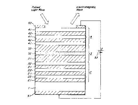
Brief Description of the Drawinq
For the better understanding of the invention,
reference is made to the accompanying drawing, in which
Fig. 1 is a diagrammatic cross sectional view showing an
05 embodiment of the solid state device for generating a
terahertz-band electromagnetic wave according to the
present invention.
In the accompanying drawing, a reference numeral
1 denotes a compound semiconductor single crystal
i substrate, 2 a first distributed Bragg reflector, 3 an
exciton generating region, 4 a second distributed Bragg
reflector, 21 and 22 first and second compound semi-
conductor layers respectively, 41 and 42 third and
fourth compound semiconductor layers respectively, 31
15 and 33 barrier layers respectively, and a reference
numeral 32 represents a quantum well layer.
Description of the Preferred Embodiments
Now a preferred embodiment of the present
invention will be described by referring to the
20 accompanying drawing hereinafter.
Fig. 1 shows an embodiment of the solid state
device for generating an electromagnetic wave in a
terahertz-band according to the present invention.
In this exemplified structure, on a compound semi-
25 conductor single crystal substrate 1 made of, forinstance GaAs, there are successively stacked a first
2 1 84682
distributed Bragg reflector 2 consisting of alternately
stacked first compound semiconductor layers 21 made of
AlAs and second compound semiconductor layers 22 made of
AlxGa(l_x)As~ an exciton generating region 3 consisting
05 of successively stacked barrier layer 31 made of AlAs,
quantum well layer 32 made of GaAs and barrier layer 33
made of AlAs, and further a second distributed Bragg
reflector 4 consisting of alternately stacked third
compound semiconductor layers 41 made of AlxGa(l_x)As and
o fourth compound semiconductor layers 42 made of AlAs.
In a concrete example of this structure, it is
preferable to select a suffix x to approximate 0.2 for
AlxGa(l-x)As-
The compound semiconductor layers forming the
15 first and second distributed Bragg reflectors 2 and 4are doped with impurities of different conductivity
types, respectively. That is to say, the compound
semiconductor layers 21 and 22 of the first reflector 2
are of one conductivity type, e.g. P-type, and the
20 compound semiconductor layers 41 and 42 of the second
reflector 4 are of the other conductivity type, e.g.
N-type. Then a spontaneous DC electric field is
produced across the exciton generating region 3.
In this manner in the present embodiment, the thus
25 generated spontaneous DC electric field is applied to
the exciton generating region 3. It should be noted
21 84682
that in general, this spontaneous DC electric field
could not provide an electric field strength by means of
which an electron and a hole of an exciton are spatially
separated from each other in an effective manner.
05 Therefore, in the present embodiment, there is provided
an electric field applying means. As shown in Fig. 1,
the electric field applying means comprises a first
electrode 51 formed on the rear surface of the substrate
1, a second electrode 52 provided on an outer surface of
the second distributed Bragg reflector 4, and a variable
DC voltage supply source 53 connected between the first
and second electrodes. It should be noted that since the
substrate 1 is made of the single-crystal compound semi-
conductor body of one conductivity type, the first
15 electrode 51 can be provided on the rear surface of the
substrate 1. Further, in order to prevent the second
electrode 52 from inhibiting the incident of the
externally impinging pulsed light wave as well as an
emission of the electromagnetic wave, the second
20 electrode is formed as a frame having a center opening.
By adjusting the variable DC voltage supply source 53,
it is possible to apply an optimum electric field across
the exciton generating region 3. In this case, a
polarity of the voltage supply source 53 may be opposite
25 to that of the spontaneous electric field. It should be
noted that in order to generate an electromagnetic wave
2 1 84682
- 10-
efficiently, a wavelength of the internally generated
light wave should be made equal to that of the externally
impinging light wave. However, in practice, a
wavelength of the internally generated light wave might
05 fluctuated due to various factors. On the other hand, a
wavelength of the internally generated light wave is
changed depending upon a strength of a static electric
field applied across the exciton generating region.
Therefore, by adjusting the variable DC voltage supply
source 53, it is possible to bring a wavelength of the
internally generated light wave into identical with that
of the externally impinging light wave, and therefore
the electromagnetic wave can be generated efficiently.
According to the invention, the first distributed
s Bragg reflector 2 is formed by stacking alternately a
plurality of first semiconductor layers and a plurality
of second semiconductor layers, said first and second
semiconductor layers having different refractive indices
from each other. Similarly, the second distributed
20 Bragg reflector 4 is formed by stacking alternately a
plurality of third semiconductor layers and a plurality
of fourth semiconductor layers, said third and fourth
semiconductor layers having different refractive indice~
from each other. In the present embodiment, the first
25 and second semiconductor layers are of one conductivity
type and the third and fourth semiconductor layers are
21 84682
of the other conductivity type. Further, the first and
fourth semiconductor layers are made of the same
material and the second and third semiconductor layers
are also made of the same material. Then, the device
05 can be manufactured easily and economically.
The aforesaid externally projected pulsed light
wave and internally generated light wave are effectively
reflected between the first and second reflectors 2 and
4. Therefore, the light wave is efficiently absorbed
o between the first and the second distributed Bragg
reflectors, the excitons are generated efficiently
within the exciton generating region situated there-
between, and a strong interaction occurs between the
internally generated light wave and the excitons.
The more differs the refractive indices between
alternately stacked semiconductor layers of two types,
the more are raised the efficiency of the reflection
effected therebetween. However, in the case that the
difference of refraction indices is not so large, it is
20 required to stack a relatively large number of semi-
conductor layers. In the present embodiment, the first
and fourth compound semiconductor layers are made of
AlAs and the second and third compound semiconductor
layers are made of Al0.2Gao.8As~ which have refractive
indices of 2.98 and 3.45, respectively. A difference in
a refractive index between these semiconductor layers is
~1 84682
-12-
not so large, and therefore in each reflector, a
relatively large number of semiconductor layers such as
twenty layers are alternately stacked. It should be
noted that according to the present invention, it is not
05 always necessary to form the first and second distributed
Bragg reflectors 2 and 4 to have identical structure.
According to the invention, the first and second
distributed Bragg reflectors 2, 4 and the exciton
generating region 3 situated therebetween constitute a
o resonator having a resonance wave length A. Then, it is
preferable to set the thickness of each layers of AlAs
and AlxGa(l_x)As in the distributed Bragg reflectors to
A/4 and to set a resonator length including the barrier
layers of AlAs and the quantum well layer of GaAs to A/2.
In the solid state device for generating a
terahertz-band electromagnetic wave according to the
present invention, the pulsed light wave of high
intensity is made incident upon the device from the side
of the second distributed Bragg reflector 4, and then
20 the terahertz-band electromagnetic wave having a high
intensity can be generated from the second distributed
Bragg reflector. In this case, the external pulsed
light wave is preferably made incident upon the second
reflector at a relatively large incident angle such as
25 about 60 degrees as shown by an arrow in Fig. l. Then,
an electromagnetic wave having a highest intensity is
2 1 84682
-13-
emitted in a direction which satisfies a reflection law
with respect to the externally impinging pulsed light
wave. That is to say, the electromagnetic wave having
the highest intensity is emitted from the second
05 reflector at an exit angle of about 60 degrees as
illustrated in Fig. l by an arrow.
In this case, the light wave having a wave
length identical with the resonant wave length of the
resonator formed by the distributed Bragg reflectors and
semiconductor layers situated therebetween, is subjected
to a multiple scattering in the resonator, as a result
of which a standing wave is formed. This standing wave
strongly interacts with the excitons in a coherent
manner, said excitons being excited in the GaAs quantum
15 well layer situated at a center of the resonator layers.
When the exciton and light wave are strongly
coupled with each other, the exciton and light wave could
not be remained in respective original physical states,
but are translated into a new physical state called
20 polariton. In the situation in which the polariton
state has been formed, the energy is periodically
exchanged between the exciton and the light wave in such
a manner that their phases are maintained unchanged.
The period of this energy exchange has a specific value
25 which is determined by the strength of the coupling,
that is, the interaction between the exciton and the
21 84~82
-14-
light wave, and the excitons are created and annihilated
repeatedly at a frequency corresponding to said period.
For example, it have been experimentally clarified that
said frequency is approximately one terahertz in the
05 above exemplified structure.
In general, it is not so easy to create and
annihilate the exciton periodically at an extremely high
frequency, particularly at a frequency of terahertz-
band. However, in the so-called polariton state, the
periodical creation and annihilation of the exciton at
the extremely high frequency can be facilitated, because
the creation and the annihilation of the exciton are a
spontaneous phenomenon accompanied with the strong
interaction between the exciton and the light wave.
On the other hand, it is a well known fact that,
when a dipole formed by positive and negative electric
charges which are spatially separated from each other is
periodically oscillated, an electromagnetic wave is
generated from this oscillating dipole. In the solid
20 state device according to the invention, in order to
separate spatially electron and hole of the exciton to
form a dipole, the electric field is applied to the
exciton generating region. In the above embodiment, the
distributed Bragg reflectors provided on respective
25 sides of the exciton generating region sides are doped
with N-type and P-type dopants, respectively, so that a
21 84682
spontaneous DC electric field is applied to the quantum
well. In addition, it is possible to control this
internally applied electric field by providing control
electrodes on outermost semiconductor layers of the
05 first and second reflectors, said control electrodes
being connected to a suitable DC bias voltage supply
source.
As mentioned above, in the above embodiment, the
spatial symmetry of the excitons is broken by the
~ electric field applied across the exciton generating
region, so that electron and hole of an exciton are
spatially separated. Accordingly, when an intense
pulsed light wave having the same wavelength as that of
the internally generated light wave is made incident
15 upon the device to excite excitons which repeat the
creation and annihilation periodically in time, an
electromagnetic wave is generated from the device.
In the solid state device for generating an
electromagnetic wave of a terahertz-band according to
20 the present invention, the light wave is confined within
the resonator, so that the light wave is subjected to
the strong interaction with the excitons generated in
the quantum well. The period of the energy exchange
between the exciton and the light wave due to said
25 strong interaction has a specific value which is
determined by the strength of the interaction between
2~ a4682
-16-
the exciton and the light wave. Therefore, a dipole
formed by spatially separated electron and hole of an
exciton is oscillated at said period to generate an
electromagnetic wave. Therefore, the electromagnetic
05 wave originated by this phenomenon presents an extremely
excellent monochromaticity. On the other hand, the
resonator of the solid device according to the invention
serves to cause a strong interaction between the light
wave confined therein and the exciton and to produce a
o standing wave of the externally impinging pulsed light
wave and hence to excite efficiently the exciton in the
quantum well layer situated at or near an anti-node
point of the standing wave. This efficient excitation
of the exciton facilitates the generation of the strong
15 terahertz-band electromagnetic wave.