Note : Les descriptions sont présentées dans la langue officielle dans laquelle elles ont été soumises.
21 85743
1 A BATTERY C~ARGER AND A PROCESS FOR A~TOMATIC ADJ~STING
2 . OPERATION OF A BATTERY CHARGER
3 BAC~GROUND OF THE INVENTION
4 The present invention relates to a process for the
automatic adjustment of a battery charger and a corresponding
6 battery charger.
7 There are known to be battery chargers which can variably
8 charge accumulator batteries and/or chargeable batteries, in
9 particular NiCd or NiMH batteries, which have different rated
voltages. In this case, in order to obtain the above-
11 mentioned variability, without manually changing the charges
12 in dependency of the rated voltage of a battery to be charged,
13 it is necessary to accept that the accumulator batteries are
14 not optimally charged if their specific rated voltage is above
or below an average rated voltage range specific to the
16 chargers.
17 It is known that such battery chargers may have a
18 monitoring unit, including, for example, a charging controller
19 such as the integrated circuit of the U2402B type as sold by
Telefunken. The charging controller serves to monitor the
21 time behavior of the charging process by monitoring the charge
22 voltage and terminates the charging process in a timely
23 fashion. To control the charging process, it is common to
24 monitor the second time derivative, generally known as
"gradient monitoring", making it possible to clearly detect
26 the areas of top-off charging and of maintenance charging by
27 monitoring the variation in time of the charge voltage.
28 If such monitoring is used on chargeable accumulator
29 batteries with different rated voltages, the instantaneous
charge voltage, which varies over a wide range depending on
31 the rated voltage of the battery being charged, must be
32 monitored.
33 Further, it is known that electronic monitoring units
34 usually are designed to monitor the specific range of the
/ 2185743
.
1 signal under surveillance where monitoring reliability is
2 optimal. If signals to be monitored lie in the boundary
3 regions or outside of this optimal range, the monitoring
4 function will be fulfilled to a certain degree, but with
decreased accuracy.
6 It is an object of the present invention to uniformly
7 charge accumulator batteries with different rated voltages at
8 an optimal rate.
9 SUMMARY OF THE lNv~.lON
In accordance with a process according to the present
11 invention, by measuring the charging voltage continuously, or
12 at specific time intervals during the charging process, the
13 assumed rated voltage of the battery being charged is
14 determined. By weighting the signal which is monitored
through amplification or deamplification, the monitored signal
16 is shifted into a signal range which is optimal for
17 monitoring. Assumptions made from mea~urements taken at a
18 beginning of the charging process should preferably be checked
19 by subsequent measurements and, if necessary, corrections
should be made.
21 By repeated or` continuous measurement of the charge
22 voltage and determination of the weighting factor in
23 accordance with the respective measurement result, an
24 incorrectly estimated rated voltage at the beginning of the
charging process may be corrected. For example, if a battery
26 with a relatively high rated voltage is deeply discharged, it
27 may be determined to have a low rated voltage initially, but
28 this determination will be corrected on the basis of a later
29 measurement. Thus, a charging process is proposed using a
flexible means to determine the rated voltage of the battery
31 being charged, thereby ensuring that the charging process is
32 performed optimally in each case.
33 In a further development of the process in accordance
34 with the present invention, it is proposed to carry out the
,
--2--
2185743
1 charging process with a controllable current source and to
2 measure the charging voltage at the beginning of the charging
3 process, thereby predetermining the charging current at the
4 beginning. With the result of such measuring, the capacity
(Ah) of the accumulator battery being charged is identified
6 and the controllable current source is correspondingly set for
7 the further charging process. Preferably, this is achieved
8 by activating pre-determined charging current versus time
9 courses according to the identified capacity, by means of
corresponding command or rated variable courses in a charging
11 current circuit negative feedback loop with the controllable
12 current source as an adjusting member.
13 The above-mentioned object is further resolved by means
14 of the battery charger.
BRIEF DESCRIPTION OF THE DRAWINGS
16 These and further features of the present invention will
17 be apparent with reference to the follo,wing description and
18 drawings, wherein:
19 FIG. 1 is a functional unit/signal flow diagram of a
battery charger according to the present invention;
21 FIG. 2 is a diagram of a controlled weighting unit for
22 a battery charger according to the present invention;
23 FIG. 3 is a functional block diagram of a battery charger
24 in accordance with the present invention;
FIG. 4 is a detailed circuit diagram of a battery charger
26 in accordance with the present invention;
27 FIG. S is a top view of the circuit board of the battery
28 charger according to the present invention with the discrete
29 components thereon;
FIG. 6 is a functional unit/signal flow diagram of a
31 battery charger incorporating a charging current control; and
32 FIG. 7 is a functional block diagram of a battery charger
33 incorporating a charging current control.
~ -3-
2 1 8574~
`_
1 DETAILED DESCRIPTION OF THE PREFERRED EMBODIMENTS
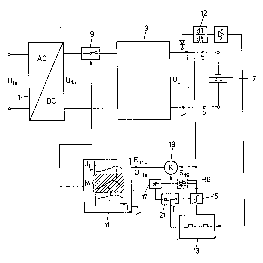
2 With reference to FIG. 1, an inpu~-side alternating
3 current V1e, is converted into a DC voltage Ula, by means of an
4 AC/DC converter 1. Via a transfer unit 3, as will be
explained further below, charging outputs 5 are fed with a
6 charging current I. A chargeable accumulator battery 7 is
7 connected to the charging outputs 5. An operating switch 9
8 enables/disables the charging process.
9 A monitoring unit 11 is supplied with a signal U1je at an
input E11,. The signal U11e is a functicn of the charging
11 voltage U~, which appears between the charging outputs 5
12 during charging of the accumulator battery 7. The monitoring
13 unit 11 monitors the charging process preferably by following
14 the time behavior of the charging voltage U~. When a given
criterion is reached or satisfied, the ~ionitoring unit 11
16 stops the charging process by sending an output signal to the
17 operating switch 9 which causes the switch 9 to move from an
18 enabling or closed position to a disablina or open position.
19 Preferably, d2Ulle/dt2, the second d,erivative of Ulle, is
determined by the monitoring unit 11. When this derivative
21 value, following the gradient monitoring methods, reaches the
22 top-off charging phase, the respective ~aintenance charge
23 phase is detected. ` Thereafter, the charging process is
24 terminated, as described hereinbefore.
As is shown schematically in FIG. 1, in the block of the
26 monitoring unit 11, the above-mentioned derivative value is
27 determined optimally only within a predetermined band or
28 signal range M. The derivative result signal is tuned to the
29 range M by comparators that detect when tne monitored signal
reaches a predetermined value. If the accu~ulator battery 7
31 being charged shows a low rated voltage U~-~ith respect to the
32 range M, the voltage UL will result in a monitored signal
33 which lies outside the measurement range ~; the same is true
34 for accumulator batteries 7 with a high rated voltaye, as
illustrated.
21 85743
1 A time control unit 13 is enabled by detection of the
2 start of a charging current I by a detection unit 12. The
3 charging voltage UL is averaged by an integration unit 15 over
4 a time span which can be preset with the time control unit 13.
The average charging voltage control signal is fed to a
6 control input S19 of a weighting unit 19 via a holding unit
7 17. Supplying the average charging voltage control signal to
- 8 the weighting unit occurs, for example, for the first time at
g the beginning of the charging process. The control unit 13
enables/disables communication of the control signal to the
11 weighting unit, as is shown schematically by a switch unit 21
12 connected to the control input S~9 via the holding unit. The
13 control signal supplied to the control input S~9 of the
14 weighting unit 19 enables the weighting unit 19 to amplify or
dampen the voltage signal UL to shift the signal Ulle into the
16 measurement band or signal range M of the monitoring unit 11.
17 By shifting the signal Ulle into the measurement band or signal
18 range M of the monitoring unit 11, the charging voltage
19 behavior is always optimally monitored, independent of the
rated voltage of the accumulator battery 7 being charged.
21 Since the discharging status of the battery is not yet
22 known, the charge voltage U~, which acts on the control unit
23 13, and which is determined at the beginning of the charging
24 process, does not nècessarily accurately identify the true
rated voltage of the accumulator battery. For example, if the
26 accumulator battery 7 is deep-discharged, a weighting is first
27 performed by the weighting unit 19, which shifts the monitored
28 signal into the measurement band or signal range M, just as
29 if the accumulator battery 7 were less discharged but had a
lower rated voltage. Therefore it is preferable that the
31 average charging voltage supplied to the weighting unit input
32 S19 is re-calculated by the integration unit 15 at repeated,
33 regular intervals. Supplying the recalculated control signal
34 to the weighting unit 19 at regular intervals will alter the
weighting or scaling factor K to correspond with changes in
36 the charge voltage U~ as the charging process proceeds. The
37 weighting factor K is thereby adjusted and corrected
..
--5--
2 1 85743
1 periodically. The result is that, the monitored signal U11e,
2 which corresponds then to the correct rated voltage of the
3 battery 7, stays centered within the measurement range M.
4 This is particularly important during the monitored time
phases toward the end of the charging process to be described
6 hereafter. The holding unit 17 supplies the current average
7 voltage control signal to the weighting unit input S19. The
8 control signal supplied by the holding unit 17 remains
9 unchanged, as does the weighting factor K, until a new control
signal is determined or calculated by the integration unit 15
11 and supplied to the holding unit 17 via the switch unit 21.
12 As should be appreciated, the adjustment of the weighting
13 factor K can be carried out either at predetermined times
14 during the charging process, at predetermined time intervals,
or continuously during the charging process. This is evident
16 from the fact that, with the time control unit 13 controlling
17 the switch unit 21, the intervals between signal connections
18 from integration unit 15 to the weighting unit input S~9 can
19 be chosen to be as short as desired. It is also possible to
directly connect the control signal output by the weighting
21 unit input S19 via a low pass filter, as is shown by dashed
22 lines in FIG. 1, to continuously supply the U~ signal to the
23 weighting unit 19.
24 FIG. 2 shows a preferred embodiment of the weighting unit
19, which is characterized by great simplicity. As discussed
26 hereinbefore, the charging voltage UL is supplied to the
27 averaging unit 15, which, in turn supplies an averaged voltage
28 control signal to the weighting unit '9 via the switch unit
29 21. The charging voltage U~ is supplied to a comparator unit
23 via the switch unit 21. The switch unit 21 is controlled
31 by the time control unit 13 and, if necessary, averaging is
32 performed at unit 15. As is shown schematically, comparator
33 unit 23 determines in which of three voltage ranges, Ba~ Bb,
34 Bc input signal resides. These ranges-are determined by
défining the comparator switching limits (not shown). The
36 comparator stage which corresponds to the input voltage
37 generates an output signal, A23" A~b~ ~3C respectively. Each
.
21 85743
1 output A23a, A23b, A23C is connected to a switch unit 25a~ 25
25C respectively. Depending on which of the outputs A~a~ A23b,
3 A23C is activated, the corresponding switching unit 25a~ 25b~
4 25C is activated. In this way the charging voltage UL is
switched to a voltage divider unit 27, which associates a
6 corresponding voltage divider value with each switch unit 25a~
7 25b~ 25c. The outputs of the voltage dividers are connected,
8 via the decoupling switch units 26a, 26b, 26C of the input E
9 to the monitoring unit 11. Corresponding switch units 25a~
26a; 25b~ 26b; 25c, 26C are closely simultaneously until another
11 f the outputs A23a, A23b' A23c is activated by the input signal
12 to the comparator unit 23, at times controlled by the timer
13 unit 13.
14 With reference to FIG. 2, it is clear that the time
control unit 13 can control the switch units 21, 25, and 26
16 as well as the integration unit 15 repetitively at a high
17 repetition frequency. Thus, if a local oscillator is used as
18 the time control unit 13 and, optionally, if the integration
19 unit 15 is not used, the weighting factor may be continuously
adjusted by the appropriate voltage divi;der value.
21 In a preferred embodiment, the voltage divider unit 23
22 is a digital potentiometer of the type manufactured and sold
23 by Xicor, e.g. via AVNET E2000 AG, Elektronische Bauelemente,
24 Bohnirainstrasse 11,~ CH-8801 Thalwil, under the trademark
E2POT Workbook, wherefrom pages 1 to 16 are incorporated
26 herein by reference to the present description and included
27 as Appendix A to the present description.
28 In the case of the preferred embodiment illustrated in
29 FIG. 2, the switch units 25 and 26 can be implemented with
analog switches. The voltage divider unit 27 is as an
31 integrated circuit. The voltage supplied to the input El~L is,
32 in each ca'se, reduced with respect to the charging voltage UL~
33 so that the measurement range M in accordance with FIG. 1 is
34 to be designed for the smallest charging voltages which are
to be monitored.
36 FIG. 3 shows a detailed signal flow and functional block
37 diagram of the invention explained thus ~ar. The AC voltage
--7--
- 21~5743
1 U1e is supplied to a band pass filter 41 comprised of an LC
2 filter, then rectified in a rectifier unit 43. Filter 41 and
3- rectifier unit 43, outlined with a dashed line in FIG. 3, form
4 the AC/DC converter 1 as shown in FIG. 1. Then the DC voltage
signal U1a is supplied from the output side of the rèctifier
6 unit 43, to the primary side of a transformatory high
7 frequency transmitter at a transmitter unit 45. The primary-
8 side signal of the transformatory transmitter unit 45 is
9 choppered by means of a MOS-FET chopper unit 47 with a
controlled duty cycle via an ohmic load unit 49 to a reference
11 potential with a pulse repetition frequency f27 of 80 kHz.
12 The duty cycle of the chopper unit 47 is controlled by means
13 of a control unit 51, which is supplied from the output
14 voltage U1a of the AC/DC converter 1.
The output signal of the transformatory transmitter 45
16 is rectified at a rectifier unit 53 and then smoothed by
17 filter unit 55. The transmitter unit 45, chopper unit 47,
18 loading unit 49, chopper-control unit 51, rectifier unit 53,
19 filter unit 55, form a controllable direct voltage source 60,
outlined with a dashed line in FIG. 3, ,which is part of the
21 transfer unit 3 shown in FIG. 1. The control input S51 to the
22 control unit 51, controls the chopper duty cycle of the
23 chopper unit 47 and thus the current output I.
24 The output A60 of the current source 60 is supplied to
one charging output 5 (see FIG. 1) for connection to an
26 accumulator battery 7 which is to be recharged. The second
27 of the outputs 5 of the charging unit is connected via a
28 current measuring unit 67 to a reference potential. The
29 charging voltage UL at the output A60 of the current source 60
is supplied to the weighting unit l9b. The weighting unit l9b
31 is constructed as shown in FIG. 2.
32 Not shown in FIG. 3 for the sake of clearness, are the
33 time control unit 13, the switch unit 21, the average value
34 .formation unit 15, the comparator unit 23, the switch units
25 and 26 and the voltage divider unit 27.
36 On the output side of the weighting unit l9b the signal
37 U11C is supplied to the input E11L of the monitoring unit lla is
, ~ ,
--8--
2 1 85743
1 preferably an integrated charging controller IC, in particular
- 2 the IC U2402B manufactured by Telefunken. The input E1,3
3 corresponds to the "sense UBATT" input of the aforementioned
4 IC.
The output A67 of the current measuring unit 67 is
6 supplied to a comparator unit 73 and, insofar as the above-
7 mentioned IC is used and the comparator unit 73 is
8 incorporated into the IC, to its "sense I-charge" input.
9 An output signal of a presetting unit 74 is also supplied
to the comparator unit 73. In the presetting unit 74, and the
11 charging current nominal or rated value is adjusted, the
12 output signal of the unit 74 is fed to the comparator unit 73
13 as a rated signal W. The signal at the output A67 of the
( 14 current measuring unit 67, is supplied to the comparator 73,
as a measured actual value signal X. On the output side of
16 the comparator unit 73 is a negative feedback control
17 difference signal a is generated. The difference signal ~ is
18 galvanically decoupled via an optical coupler unit 71 and
19 applied to the control input S51 of the control unit 51.
The rated signal W from the prssetting unit 74 is
21 generated from an output signal of a reference voltage
22 generator 79 generated from a stabilized reference voltage
23 source. The generator 79 is fed via a separate supply circuit
24 81 and via a transformatory transmitter 83 from the AC voltage
U1e.
26 A temperature measuring unit 86, preferably in the form
27 of an NTC resistor, is thermally coupled to the accumulator
28 battery 7 to be charged, and attached to a holder 85 for the
29 accumulator battery 7 to be charged. A temperature-dependent
output signal A86 from the temperature measuring unit 56 is
31 supplied to the monitoring unit lla for monitoring purposes.
32 In order to detect if an accumuiator battery 7 is
33 actually a rechargeable battery or a non-rechargeable battery,
34 a detector 87 is preferably provided in the holder 85. The
detector 87 recognizes if the charging process is permissible
36 or not on the basis of specific marks on the battery housing,
37 such as barcodes or specific mechanical configurations of the
_ 9 _
2 1 85743
1 housing, such as notches. Detector 87 activates/deacti~ate-s
2 a charging operating switch 9, sh~wn in FIG. 1 but not shown
3 in FIG. 3-.
4 It is also possible for the detector 87 to trans~it the
necessary monitoring data, and/or control information dir-ectl~
6 to the monitoring unit lla, or to the control unit for the
7 direct voltage source 60, if the corresponding information is
8 provided on the batteries to be charged.
9 FIG. 4 shows the circuit diagram of a battery cha~ger
constructed in accordance with the principle of the invention
11 as shown in FIG. 3.
12 The following is a list of the values of the discrete
13 electronic elements:
14 RESISTORS
ROl 10 Kn R14 10 Kn R27 10 ~n
16 RO2 10 Kn R15 8 Q R28 16 Rn
17 RO3 2.7 Kn R16 22 n R29 3.3 Kn
18 RO4 12 Rn R17 47 n , R30 0.01 n
19 RO5 82 n R18 47 n R31 10 Kn
RO6 22 n Rl9 10 n R32 100 Kn
21 RO7 10 Kn R20 2.2 Kn R33 820 n
22 RO8 1 KQ `R21 56 KQ R34 1.5 Kn
23 RO9 4.7 n R22 10 Kn R35 510 n
24 R10 470 Kn R23 470 Kn R36 2.4 Kn
Rll 56 Kn R24 2.2 Kn R37 trimmer 2Kn
26 R12 0.39 n R25 15 Kn R43 resistor 56Kn
27 R13 10 Kn R26 6.8 KQ
--10--
2 1 85743
, .
1 CAPACITORS
2 COl 0.47 ~F C10 4.7 nF Cl9 220 ~F
3 C02 1 nF Cll 100 nF C20 1 ~F
4 C03 1 nF C12 470 pF C21 470 nF
S C04 150 ~F C13 1 nF C22 10 ~F
6 C0S 4.7 F C14 1 nF C23 1 nF
7 ~C06 4.7 F C15 1 nF C24 22 ~F
8 C07 100 ~F C16 1 nF C25 22 nF
9 C08 100 nF C17 1 nF C26 220 ~F
CO9 10 nF C18 1 nF C27 100 ~F
C28 22 ~F
11 DIODES
DO8 z-diode ZPD22
12 DOl diode DF-OlM DO9 diode lN4148
13 DO2 diode lN4007 DO10 LED diode GREEN
14 DO3 diode lN4148 DOll LED diode RED
DO4 z-diode ZPD22 DO12 di~de KBU 4K
16 D05 diode RGP 15M DO13 diode lN4007
17 DO6 diode RGP 15M
18 DO7 diode BYW 99
19 PI-200/FEP 30DP
INTEGRATED CIRCUIT
21 ICl SGS-THOMSON UC3842N IC5` SIEMENS CNY17F3
22 IC2 ITC 9504-A TOl SGS-THOMSON
23 IC6 ITC-AR 9509-AR POWER MOS-FET SDS-DElE-M
24 IC3 SGS/NATIONAL LM358AN RELl SDS
IC4 SGS/NATIONAL LM78LO5
--11--
2 1 85743
1 INDUCTORS
2 L01 TIMONTA SPOOL 2X27 HY-DFKY, 2-31-1.4-27A
3 L02 HARTU THROTTLE 200025-14-10.0 A/250V, 0,30MH/GKK
4 TRANSFORMERS
TR1 TRANSFORMER FERRIT PG3-2/30-H7C4
6 TR2 TRANSFORMER 220V/12 V-1.5, VA-50-60HZ
7 FUSES
8 Fl FUSE 1.60 AT
~,
9 FIG. 5 shows a top view of a printed circuit for
realizing the battery charger according to FIGS. 1-4.
11 With the battery chargers in accordance with the
12 invention described it was possible to charge batteries in a
13 rated-voltage range between 1.2 V and 14.4 V, and preferably
14 between 2.4 V and 14.4 V, with around 7.$ A and in a charging
time of around 10 min. at an optimal rate.
16 In a preferred form of constructional realization, all
17 the connecting lines and electronic components, which treat
18 low level measuring, monitoring etc., signals are grouped on
19 one circuit board as one low level module. All elements and
connecting lines treating higher value current and voltages
; 21 are realized on a second board as a second module, and the two
22 modules are linked in a removable manner. This has the
23 advantage that further improvements and amendments to the
24 circuitry, which are primarily directed to the low level
signal processing, may be realized on one of the modules which
26 may easily be exchanged leaving the high level current module
27 unchanged. The low level module is thereby preferably
28 realized in thick film technique.
29 Up to now the process invented was explained with a focus
on optimal adjustment of the battery charger to different
31 rated voltages of an accumulator battery to be charged. The
-12-
2 1 857~3
.
l battery charger, and/or process, in accordance with the
- 2 invention, is now further improved taking into account
3 different capacities (Ah) of the accu~ulator battery. This
4 will be explained by means of FIG. 6, which, based on the
S presentation in FIG. 1, shows the main principles of this
6 further development.
7 As shown in FIG. 6, the charging voltage UL is supplied
8 to a differentiation unit 90. At an output A~o of the
g differentiation unit so, a signal is generated with a level
which is dependent on the variation of UL over time t.
11 Analogous to the average value formation or integration unit
12 15, an average value formation unit 92 is provided, which
13 forms the average value of the differentiation result, during
14 a time span controlled by time control unit 13.
Controlled by the time control unit 13, a switch unit 94
16 switches the average value result of the differentiated signal
17 to a memory unit 96. The signal fed to unit 96 is designated
18 as U. Depending on the value of the signal U, (for example
19 corresponding to the initial rise of the charging voltage UL
determined over a predetermined time spa~?. Unit 96 activates
21 a predetermined charging current behavior function IX(t) that
22 controls a controllable current source 60a via its control
23 input S60a, at the transmission unit 3. Thereby, a conclusion
24 is drawn with regard~to the capacity of the battery 7 being
charged, which is defined by the UL-time derivative,
26 particularly from the initial charge behavior, and
27 correspondingly an optimal charging current time-behavior is
28 controlled at the current source 60a, which may be a constant
29 charging current.
If one considers the embodiment shown in FIG. 3 with the
31 use of a charging controller-IC of the above-mentioned type
32 as a monitoring unit lla, it becomes clear that the
33 improvement in accordance with FIG. 6 may be directly realized
34 by replacing the adjusting unit 74 for controlling the
charging current at the current source 60 (FIG. 3) by a
36 control with the unit 96 in accordance with FIG. 6.
-13-
2 ~ 85743
`
1 FIG. 7 illustrates an improvement in accordance with FIG.
2 6 based upon the embodiment shown in FIG. 3.
3 In FIG. 7, the charging voltage UL is fed to a battery
4 identification unit 98, which includes the units 15, 21, 23
shown in FIG. 2, and the units 90, 92, and 94 shown in FIG.
6 6, as well as the control unit 13 shown in FIG. 1. On the
7 output side of the identification unit 98 there appears in
8 accordance with FIG. 2, a signal l9b supplied to the weighting
g unit S19b, and the signal U, which is supplied to the charging
current course selection unit 96, in accordance with FIG. 6.
-14-