Note : Les descriptions sont présentées dans la langue officielle dans laquelle elles ont été soumises.
00161!1008
216921
DISCHARGE LAMP HAVING LIGHT-TRANSMISSIVE CONDUCTIVE
s COATING FOR RF CONTAINMENT AND HEATING
Field of the Invention
This invention relates to low pressure discharge lamps which are
energized by high frequency electrical energy and, more particularly, to
discharge lamps having a light-transmissive conductive coating. The
invention is particularly useful in vehicles for neon lamp assemblies which
may require RF containment, and for fluorescent lamp assemblies which
may require heating and RF containment.
Background of the Invention
It has become customary in automobiles and other vehicles to utilize a
stop/brake light which is located high on the rear of the vehicle and is
centered for improved visibility. The stop light may, for example, be located
in the rear window. In sport-utility vehicles which have a tailgate, the stop
zo light may be located above the rear window. Such stop lights are typically
elongated and may be 20 or more inches long. In order to achieve uniform
illumination over this length, neon lamps may be used. In general, neon
lamps have relatively low power consumption and long operating lives.
It has been proposed in the prior art to use neon lamps for signaling in
as vehicles. A neon lamp direction signal, including arrows for indicating
direction, is disclosed in U.S. Patent No. 1,792,599 issued February 17,
1931 to Murray. The disclosed lamp also includes a stop signal indication.
A neon sign, including a neon lamp tube for mounting in the window of an
automobile, is disclosed in U.S. Patent No. 1,854,654 issued April 19, 1932
3o to Koch, Jr. et al. A neon lamp signaling device for mounting in the rear
window of a vehicle is disclosed in U.S. Patent No. 1,839,499 issued
_2_ 2 ~ X6921
January 5, 1932 to Rava. A rare gas automobile indicator light system
employing a single horizontally disposed indicator tube operated to provide
braking, parking, emergency flasher and tum indications is disclosed in U.S.
Patent No. 4,682,146 issued July 21, 1987 to Friedman, III.
Neon lamps may be energized at a frequency on the order of 60
kilohertz. The starting voltage may be on the order of 3 kilovolts, and the
operating voltage may be on the order of 1 kilovolt. It is important to insure
that the neon lamp assembly does not emit radiation which may potentially
interfere with nearby electronic equipment in the vehicle, in other vehicles
and in adjacent buildings. In one prior art neon lamp assembly, the light
transmitting aperture is covered with a conductive mesh that substantially
blocks emission of RF radiation generated within the lamp assembly.
Subminiature fluorescent lamps utilized in vehicles may be operated
at a frequency in the range of 17 to 35 kHz. It is important to insure that
such subminiature fluorescent lamps do not emit radiation which may
produce interference as described above.
A pilot lamp fixture having a transparent conductive shield positioned
in front of the pilot lamp for reducing or eliminating RF interference is
disclosed in U.S. Patent No. 3,801,808 issued April 2, 1974 to Johnson. A
zo headlamp for motor vehicles, including a gas discharge lamp, a glass or
plastic screen and a transparent metallic coating on the discharge lamp or
on the screen for shielding interference radiation, is disclosed in U.S.
Patent
No. 5,287,258 issued February 15, 1994 to Remus. Fluorescent lamps
having a transparent, electrically-conductive coating on the inner surface of
ZS the lamp envelope for reducing ignition voltage are disclosed in U.S.
Patent
No. 3,963,954 issued June 15, 1976 to Milke et al; U.S. Patent No.
3,967,153 issued June 29, 1976 to Milke et al; U.S. Patent No. 4,020,385
issued April 26, 1977 to Lagos and U.S. Patent No. 4,500,810 issued
l 1023.1
-3- 2 i 8692 i
February 19, 1995 to Graff. A low pressure mercury vapor discharge lamp
having an interference-suppressing transparent conductive layer on its inside
surface is disclosed in U.S. Patent No. 4,568,859 issued February 4, 1986 to
Houkes et al. The conductive layer is connected to an electric supply lead-in
wire.
Subminiature fluorescent lamps may be utilized in an environment
where they are subjected to low temperatures. For example, subminiature
fluorescent lamps may be utilized for illumination of instrument panels in
vehicles. Under these conditions, temperatures of -40°F or lower may be
encountered. At such low temperatures, the fluorescent lamp may have a
long warm-up time before reaching full light output. Thus, it may be
necessary to provide a lamp heater. In the prior art, a heater comprising a
flexible printed circuit having a heating element formed thereon has been
attached to the fluorescent lamp with an adhesive. However, the printed
~s circuit heater occasionally lifts off the fluorescent lamp. In addition,
the
limited thermal transfer between the printed circuit heater and the lamp
requires a relatively high power input to the heater.
A heater for a glass substrate including an electrically-conductive
transparent film is disclosed in U.S. Patent No. 4,970,376 issued November
Zo 13, 1990 to Mellor et al. A window defogging system including an indium tin
oxide heater is disclosed in U.S. Patent No. 5,354,966 issued October 11,
1994 to Sperbeck. A glazed window which includes a transparent
conductive coating for heating is disclosed in U.S. Patent No. 3,609,293
issued September 28, 1971 to Stewart et al.
2s
Summar~i of the Invention
According to a first aspect of the present invention, a lamp assembly
comprises a housing having an aperture for emission of light and a
11023.1
216921
discharge lamp mounted within the housing for emission of light through the
aperture. The discharge lamp includes an elongated tubular lamp envelope
containing a fill material for supporting a light-emitting discharge and
electrodes mounted at opposite ends of the lamp envelope. The lamp
assembly further comprises a light-transmissive conductive coating on the
lamp envelope for substantially attenuating emission of RF energy from the
discharge lamp during operation and a conductor in electrical contact with
the conductive coating for coupling the conductive coating to a reference
potential, such as ground.
The light-transmissive conductive coating may comprise indium tin
oxide. The conductor may be in contact with the conductive coating along a
substantial portion of the length of the lamp envelope to provide a low
impedance connection between the conductive coating and ground. In one
embodiment, the conductor comprises a metal strip in electrical contact with
~s the light-transmissive conductive coating along the length of the lamp
envelope. In a second embodiment, the conductor comprises a conductive
silicone strip in electrical contact with the light-transmissive conductive
coating along the length of the lamp envelope. In a third embodiment, the
conductor comprises a reflective coating on a portion of lamp envelope to
2o control the light distribution pattern of the discharge lamp. The
reflective
coating may be patterned to define an aperture for emission of light from the
discharge lamp. The conductor may further comprise a conductive silicone
tube positioned around an end of the lamp envelope in electrical contact with
the light-transmissive conductive coating. The conductive silicone tube
is provides a non-abrasive contact to the conductive coating.
Electrical energy may be coupled to the electrodes of the discharge
lamp through a coaxial cable having a center conductor and an outer shield.
In this embodiment, the center conductor is electrically connected to one of
t 1023.1
_ 2186921
-5-
the electrodes of the discharge lamp, and the outer shield may be electrically
connected to the light-transmissive conductive coating. A conductive
silicone tube positioned around an end of the lamp envelope may be used to
electrically interconnect the conductive coating to the outer shield of the
coaxial cable. The lamp assembly may further include a transformer
positioned adjacent to and electrically connected to one of the electrodes,
and a power source for supplying electrical energy to the transformer.
According to another aspect of the invention, the discharge lamp
comprises an elongated tubular lamp envelope containing a fill material for
supporting a 1'~ght-emitting discharge and electrodes mounted at opposite
ends of the lamp envelope, a light transmissive conductive coating on the
lamp envelope for substantially attenuating emission of RF energy during
operation and a low impedance conductive strip on the lamp envelope along
a substantial portion of its length. The conductive strip ~ in electrical
contact
is with the fight-transmissive conducctive coating for low impedance coupling
of
the conductive coating to a reference potential.
According to a further aspect of the invention, a lamp assembly
comprises a discharge lamp including an elongated tubular lamp envelope
containing a fill material for supporting a light~mitting discharge and
2o electrodes mounted at opposite ends of the lamp envelope, a light
transmissive conductive Wing on the lamp envelope for substantially
attenuating emission of RF energy from the discharge lamp during operation,
a conductor for coupling the conductive coating to a refierence potential, a
power source for supplying electrical energy to the discharge lamp, and
2s means for coupling the electrical energy from the power source to the
electrodes.
According to still another aspect of the invention, the light
transmissive conductive coating and/or the conductive strip on the lamp
11023.1
2 i ~b92 i
envelope may be used for heating of fluorescent discharge tamps, as well as
for RF containment. An electrical circuit supplies current to the conductive
strip and/or the conductive coating when the discharge lamp is below a
predetermined temperature. The current produces heating of the discharge
s lamp. The electrical circuit may comprise a DC power source and a thermal
switch connected between the DC power source and the conductive strip
and/or the conductive coating. Other sensing techniques, such as
monitoring lamp performance, may also be utilized.
Brief Description of the Drawings
For a better understanding of the present invention, reference is made
to the accompanying drawings, which are incorporated herein by reference,
and in which:
FIG. 1 is a top view of a lamp assembly in accordance with a first
~s embodiment of the invention;
FIG. 2 is a cross section of the lamp assembly of FIG. 1;
FIG. 3 is a cross section of a discharge lamp in accordance with a
second embodiment of the invention;
FIG. 4 is a cross section of a discharge lamp in accordance with a
2o third embodiment of the invention;
FIG. 5 is an electrical schematic diagram of the lamp assembly of
FIG. 1;
FIG. 6 is an electrical schematic diagram of a lamp assembly in
accordance with another embodiment of the invention;
2s FIG. 7 is a pictorial representation of one end of a discharge lamp in
accordance with the invention, illustrating the electrical connections to the
discharge lamp;
FIG. 8 is a cross-sectional view of the lamp assembly shown in FIG.
11023.1
-7- 2 i 8692 ~
7;
FIG. 9 is a partial cross-sectional view of another embodiment of a
lamp assembly in accordance with the invention;
FIG. 10 is a graph of RF emission level as a function of frequency for
a prior art discharge lamp;
FIG. 11 is a graph of RF emission level as a function of frequency for
a discharge lamp in accordance with the invention; and
FIG. 12 is a schematic representation of another aspect of the
invention wherein a conductive coating and a conductive strip are is used for
heating and RF containment in a fluorescent lamp.
Detailed Descru~
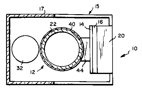
A lamp assembly 10 in accordance with a first embodiment of the
invention is shown in FIGS. 1 and 2. The lamp assembly 10 includes a
~s discharge lamp 12 mounted in a lamp housing 15, shown schematically in
FIG. 2, having a light-transmissive portion 17 for emission of light from
discharge lamp 12. A ground plane 14 and an insulator 16 are mounted in
housing 15 behind discharge lamp 12. A ballast circuit 20, which may be
mounted on the rear of insulator 16, is connected to one electrode of
Zo discharge lamp 12 through a high voltage step-up transformer 30. The
ballast circuit 20 supplies electrical energy of suitable voltage and
frequency
for starting and operating the discharge lamp 12. The ballast circuit 20 may
be provided with thermally conductive fins 21 to assist in temperature
control. An optical element 32, such as a rod or fens, may be positioned in
2s front of the discharge lamp 12 to modify the emitted light pattern.
The lamp assembly 10 may have an elongated configuration
designed for use as a stop light in a sport utility vehicle or other vehicle.
The
lamp assembly may have an overall length on the order of 20 inches or
1 I 023.1
CA 02186921 2003-11-12
_ g _
more. It will be understood that the lamp assembly 10 can have other
dimensions and form factors within the scope of the present invention.
The discharge lamp 12 includes an elongated lamp envelope 22
having electrodes 24 and 26 sealed therein at opposite ends. The
discharge lamp contains a fill material for supporting a light-emitting
discharge. In a preferred embodiment, the discharge lamp 12 is a neon
lamp. Each electrode is connected through a press seal to an external
contact pin. In a preferred embodiment, the lamp envelope 22 has an
outside diameter of about 5 millimeters. A preferred fill material
includes neon at a fill pressure from 100 +I-15 torr.
A 20 inch neon lamp may be operated at a frequency of 60 kHz
and a voltage of about 1000 volts, with a required starting voltage of
about 3000 volts. It will be understood that neon lamps having different
lengths and fill pressures will require different starting and operating
I S voltages.
In the discharge lamp 12, a high electric field is induced in the
region of each electrode by the applied voltage. Since an AC voltage is
applied to the lamp, the lamp acts as a dipole radiation source. To
induce discharge in relatively high pressure lamps, relatively high
voltages are needed. Also, relatively high voltages are required for
inducing discharge in long lamps. As a result, high pressure, long lamps
have a stronger induced dipole radiation. In the example described
above, the neon lamp requires an operating voltage of about 1000 volts
and a starting voltage of about 3000 volts. The dipole radiation is
primarily at the fundamental frequency of lamp operation, typically 60
kHz. Due to resonances, plasma banding, and material-induced delays,
harmonics and frequency spreading occur. A 60 kHz neon lamp may
emit radio frequency (RF) noise at 60 kHz±5 kHz; 120 kHz±20 kHz;
240
-9- 218b921
kHz t 60 kHz; etc. In general, longer and more powerful lamps emit more
RF noise.
In accordance with one aspect of the invention, the lamp envelope 22
is coated with a light-transmissive conductive coating 40, which functions as
s an RF shield. As discussed below, the conductive coating 40 is electrically
connected to a reference potential, such as ground, and substantially
attenuates RF noise generated within the discharge lamp 12. A preferred
conductive coating 40 is indium tin oxide (ITO). The ITO coating may have a
thickness selected to provide a conductivity of about 200 - 1000 ohms per
square centimeter and is preferably applied to the lamp envelope 22 by
dipping. This ITO coating attenuates the light output from the neon lamp by
about 10% - 20%. Other suitable light-transmissive conductive coatings may
include very thin metals, fluorine-doped tin oxide and zinc oxide.
As noted above, the conductive coating 40 is electrically connected to
~s a reference potential, such as ground. Over the length of a 20 inch
discharge lamp, the impedance of the conductive coating 40 is not negligible
and may be sufficient to result in a loss of RF shielding effectiveness. As
known in the art, RF shielding is most effective for a shield with a low
electrical impedance at frequencies where RF shielding is required. In
2o accordance with a further aspect of the invention, a low impedance
conductor is in electrical contact with the conductive coating 40 over all or
a
portion of the length of the lamp envelope 22. In the embodiment of FIGS.1
and 2, a conductive silicone strip 44 with low electrical impedance is
positioned between ground plane 14 and discharge lamp 12 and contacts
25 the conductive coating 40 over a major portion of the length of the lamp
envelope 22. Thus, the conductive silicone strip 44 provides a low
impedance electrical connection between conductive coating 40 and ground
plane 14 along the length of the lamp envelope. The silicone strip 44 is
11023.1
-10- 2186921
preferably resilient to insure contact with conductive coating 40 and to
provide cushioning for the discharge lamp 12, and preferably has a
resistance of less than one ohm per inch. A commercially available
conductive silicone may be used.
It will be understood that the lamp assembly shown in FIGS. 1 and 2
and described above is given by way of example and is not limiting as to the
scope of the present invention. A wide variety of different housing
configurations can be utilized. Furthermore, the ballast circuit 20 and the
transformer 30 may be mounted remotely from the discharge lamp 12. As
described below, RF noise emission from the lamp assembly is reduced
when the ballast and the transformer are mounted in close proximity to the
discharge lamp.
A second embodiment of a discharge lamp in accordance with the
present invention is shown in FIG. 3. Like elements in FIGS. 2 and 3 have
the same reference numerals. In the embodiment of FIG. 3, a metal strip 50
is in contact with conductive coating 40 over all or a substantial portion of
the
length of the lamp envelope 22. The metal strip 50 provides a low
impedance electrical contact to the conductive coating 40. The metal strip
50 is connected, as described below, to a reference potential, such as
2o ground. The metal strip 50 may be deposited directly on conductive coating
40 and is positioned on the lamp envelope 22 to minimize blockage of useful
light output. Thus, the metal strip 50 may have a minimum width that
provides the desired impedance and may be positioned facing the opaque
portion of the housing. In a preferred embodiment, the metal strip is
Zs aluminum and may be applied to the lamp envelope 22 by evaporation or
painting.
A third embodiment of a discharge lamp in accordance with the
present invention is shown in FIG. 4. Like elements in FIGS. 2 and 4 have
l 1023.1
-11- 2186921
the same reference numerals. In the embodiment of FIG. 4, a metal strip 54
provides a low impedance electrical contact to conductive coating 40 and is
connected to a reference potential, such as ground. The metal strip 54
additionally functions as a reflective coating on lamp envelope 22 and
defines an aperture 56 for emission of light from the discharge lamp. The
metal strip 54 covers all of the lamp envelope 22 except aperture 56 and has
a reflective inside surface, so that light generated within the discharge lamp
is reflected through aperture 56.
The electrical connections of the lamp assembly of FIGS. 1 and 2 are
shown in the schematic diagram of FIG. 5. One output terminal of the ballast
circuit 20 is connected through transformer 30 to electrode 24. The other
output terminal of the ballast circuit 20 is connected to electrode 26 and to
ground. The conductive silicone strip 44, which electrically contacts the
conductive coating 40 over the length of lamp envelope 22, is electrically
connected to ground. In an alternate configuration, a step-up transformer
may be required at each end of the discharge lamp 12. In this configuration,
electrode 26 is not grounded, and a balanced voltage is applied to the
discharge lamp 12.
Another embodiment of the invention, wherein the ballast circuit 20 is
20 located remotely from the discharge lamp 12, is shown schematically in FIG.
6. The terminals of the ballast circuit 20 are connected to electrodes 24 and
26 of discharge lamp 12 by coaxial cables 60 and 62, respectively. Coaxial
cable 60 includes a center conductor 64 connected between one output
terminal of ballast circuit 20 and electrode 24, and an outer conductor 66
that
as is grounded. Coaxial cable 62 includes a center conductor 68 that is
connected between the other output terminal of ballast circuit 20 and
electrode 26, and an outer conductor 70 that is grounded. The light-
transmissive conductive coating 40 and silicone strip 44 are electrically
11023.1
-12_ 2186921
connected to outer conductors 66 and 70 of coaxial cable 60 and 62,
respectively, to provide substantially continuous RF shielding of the lamp
assembly from the ballast circuit 20 to and including discharge lamp 12. As
noted above, the discharge lamp 12 may be energized with a balanced
voltage as shown in FIG. 6 or may utilize a single-ended drive wherein one
of the electrodes is grounded, as shown in FIG. 5.
In the embodiment of FIG. 6, step-up transformers are located in
ballast circuit 20, and the required starting and operating voltages are
transmitted through coaxial cables 60 and 62 to discharge lamp 12. In an
alternative configuration, a step-up transformer may be mounted in close
proximity to one or both electrodes of discharge lamp 12. A coaxial cable is
connected between each step-up transformer and the remotely located
ballast circuit.
In summary, several configurations may be utilized. The ballast circuit
20 may be located in close proximity to the discharge lamp 12 or may be
located remotely. An advantage of mounting the ballast circuit close to the
discharge lamp is that lead lengths are minimized and RF shielding is easier.
An advantage of remote location of the ballast circuit is that the ballast
circuit
can be used to energize two or more discharge lamps in different locations.
2o In addition, practical considerations, such as available space, may dictate
remote location of the ballast circuit. When the ballast circuit is remotely
located, the connections to the discharge lamp are preferably made by
coaxial cable, with the outer conductor of the coaxial cable connected to the
conductive coating on the discharge lamp to provide continuous RF shielding
25 to the extent possible. Furthermore, step-up transformers may be connected
to one or both electrodes of the discharge lamp, depending on whether a
grounded or a balanced drive configuration is utilized. The step-up
transformer or transformers may be located in the ballast circuit or, more
11023.1
preferably, are located in close proximity to the electrodes of the discharge
lamp to which they are connected. In each case, the RF shielding is
provided on the discharge lamp and the electrical connections to the ballast
circuit. Preferably, the ballast circuit is also shielded to reduce RF
emissions.
In the configurations shown in FIGS. 5 and 6 and described above,
the silicone strip 44 can be replaced with metal strip 50 shown in FIG. 3 or
metal strip 54 shown in FIG. 4. In addition, when the conductive coating 40
has sufficiently high conductivity to provide effective RF shielding, the
conductive coating alone can be utilized, with the conductive coating
connected to a reference potential, such as ground, at one or both ends of
the discharge lamp.
A preferred configuration for connecting the discharge lamp 12 to the
coaxial cable 60 is shown pictorially in FIG. 7. The coaxial cable 60 includes
~s center conductor 64, outer conductor 66, typically in the form of a braided
wire, and an insulator 72 between center conductor 64 and outer conductor
66. The coaxial cable also includes an outer jacket 74 surrounding outer
conductor 66. The center conductor 64 is electrically connected to electrode
24 by attaching it to the lead wire which extends from electrode 24 through
Zo lamp envelope 22. The connection between center conductor 74 and the
lead wire is surrounded with an insulator 76 such as silicone.
The conductive coating 40 on the outer surface of lamp envelope 22
is preferably connected to outer conductor 66 by a conductive silicone tube
80. As shown in FIG. 7, the conductive coating 40 preferably covers the
2s main portion of lamp envelope 22 except for a seal region 82 near the
electrode leads and preferably extends at least slightly beyond the electrode
24 toward seal region 82. The conductive silicone tube 80 provides a
nonabrasive and reliable electrical connection to conductive coating 40.
I 1023.1
2186921
-14-
When the discharge lamp 12 includes a metal strip as shown in FIGS. 3 and
4 or a silicone strip as shown in FIG. 2, the silicone tube 80 is in
electrical
contact with both the conductive coating 40 and the metal or silicone strip.
Preferably, the silicone tube 80, in its unstretched state, is smaller in
diameter than lamp envelope 22. The silicone tube 80 is stretched to a
larger diameter to place it over lamp envelope 22, and the resilience of
silicone tube 80 provides secure electrical contact with the conductive
coating 40 and any metal or silicone strip that may be present on lamp
envelope 22. The silicone tube 80 may be positioned inside the outer
conductor 66 of coaxial cable 60, as shown in FIG. 7, or may be positioned
outside outer conductor 66. The outer conductor 66 and the silicone tube
may be secured in electrical contact by a heat shrinkable tube 84.
Optionally, a heat shrinkable tube may also be used to secure the silicone
tube 80 in electrical contact with conductive coating 40. The configuration
shown in FIG. 7 and described above provides a continuous RF shield
around the lamp envelope 22, through the silicone tube 80 and the outer
conductor 66 of coaxial cable 60 to the ballast circuit, thus providing
substantial attenuation of RF noise.
A cross section of the assembly of FIG. 7 through the electrode 24 is
Zo shown in FIG. 8. The conductive coating 40 is surrounded by conductive
silicone tube 80, thus providing a large area, nonabrasive electrical contact.
In the embodiment of FIG. 8, a metal strip 86, is provided along the length of
lamp envelope 22. As shown, the silicone tube 80 makes electrical contact
with metal strip 86, thus providing a low impedance contact to the conductive
Zs coating 40 along the length of the lamp envelope 22.
The conductive tube 80 provides a reliable, nonabrasive, large area
electrical contact to the conductive coating 40. In addition, the silicone
tube
80 is resilient and can be used for shock resistant mounting of the discharge
11023.1
~'8692i
-15-
lamp 12. The silicone tube 80 as well as the silicone strip 44 conduct heat
from the discharge lamp. The ITO conductive coating on the lamp envelope
provides a shield to reduce RF noise emission and is oxidation and abrasion
resistant.
s An alternative configuration for connecting the coaxial cable to the
discharge lamp is shown in FIG. 9. Like elements in FIGS. 8 and 9 have the
same reference numerals. The center conductor 64 of coaxial cable 60 is
connected to electrode 24 as described above. In this configuration, the
outer conductor 66 of coaxial cable 60 is in direct contact with conductive
coating 40. The connection between coaxial cable 60 and discharge lamp
12 is secured by a heat shrinkable tube 90 which maintains electrical contact
between outer conductor 66 and conductive coating 40.
The effectiveness of the present invention in reducing RF noise
emission from a neon lamp assembly is illustrated in FIGS. 10 and 11. Each
of FIGS. 10 and 11 is a graph of RF emission level as a function of
frequency. FIG. 10 illustrates the RF emission from an 18 inch neon tamp
without a conductive coating operated at 3000 volts and 60 kHz (30 watts
system power). FIG. 11 illustrates the RF emission from a neon lamp
operated in the same manner having an indium tin oxide coating and a metal
zo coating which defines an aperture, as shown in FIG. 4. The RF emission
levels were measured in a certified testing Laboratory. In FIGS. 10 and 11, a
fine 94 represents a specification for a maximum acceptable level of RF
emission over the frequency range. As shown in FIG. 10, the neon lamp
without a conductive coating exceeds the specification significantly. The
25 neon lamp having a conductive coating meets the specification over the
entire frequency range, as shown in FIG. 11.
In accordance with a further aspect of the present invention, the light-
transmissive conductive coating and/or the metal or silicone strip that
I 1023. t
-16- 2186921
contacts the conductive coating may be used as a heater for fluorescent
lamps that may be subjected to tow temperatures. As shown in FIG. 12, A
subminiature fluorescent lamp 110 is provided with a light-transmissive
conductive coating 112, such as ITO, and a conductive strip 114, such as a
metal strip or a conductive silicone strip. The electrode leads of the
fluorescent lamp 110 are connected to a ballast circuit 116 which supplies
electrical energy for lamp operation. The conductive strip 114 is connected
at one end to ground and is connected at the other end through a thermal
switch 120 to a DC source 122. Insulators 124 and 126, shown
schematically in FIG. 12, isolate the voltage applied to fluorescent lamp 112
by ballast circuit 116 from the DC voltage applied to conductive strip 114.
The thermal switch 120 may be positioned to sense the temperature
of fluorescent lamp 112. When the temperature of the fluorescent lamp 112
is below a predetermined temperature, thermal switch 120 closes and
connects DC source 122 to the conductive strip 114. When the thermal
switch 120 is closed, an electrical current passes through conductive strip
114 and conductive coating 112, thereby heating fluorescent lamp 110.
When the fluorescent lamp 110 is heated above the predetermined
temperature or the ambient temperature is above the predetermined
2o temperature, the thermal switch 120 opens, thereby discontinuing heating of
fluorescent lamp 112.
The heating of fluorescent lamp 112 is produced by the electrical
resistance of conductive strip 114 and conductive coating 112. The
resistance is selected based on the voltage of DC source 122, the length
as and diameter of fluorescent lamp 112, the expected minimum temperature
and the desired power level. By way of example, a 4 inch fluorescent lamp
can be heated at a power level of 3.5 watts, a voltage of 12.8 volts and a
resistance of conductive strip 114 of about 40-50 ohms. The resistance
11023.1
_ 2186921
-17-
value required for heating is sufficiently low to provide effective RF
shielding.
The conductive strip 114 and the conductive coating 112 are
connected to ground whether the thermal switch 120 is open or closed.
Thus, the conductive coating 112 and the conductive strip 114 provide
s effective RF shielding of the fluorescent lamp 112, as well as heating of
fluorescent lamp 112.
The conductive coating 112 and the conductive strip 114 provide
more efficient transfer of heat to fluorescent lamp 112 than the prior art
printed circuit heater. The conductive coating 112 assists in the transfer of
heat around the diameter of the lamp. Thus, there are no cold spots for
mercury to recondense within the fluorescent lamp. For a 4 inch fluorescent
lamp at -40°C, 50% of full light output was achieved in less than 20
seconds
using a conductive strip powered at about 3.5 watts. This was less than one
third of the power required for heating of the same lamp with the prior art
~s printed circuit heater.
It will be understood that different circuit configurations can be used
for heating fluorescent lamp 112 by passing an electrical current through the
conductive strip 114 and the conductive coating 112. For example, various
types of thermal switches and other control circuits may be utilized. Sensing
Zo of lamp performance may be utilized as an alternative to sensing of lamp
temperature.
While there have been shown and described what are at present
considered the preferred embodiments of the present invention, it will be
obvious to those skilled in the art that various changes and modifications
zs may be made therein without departing from the scope of the invention as
defined by the appended claims.
11023.1