Note : Les descriptions sont présentées dans la langue officielle dans laquelle elles ont été soumises.
21 87477
SELF ALIGN LEADFRAME
Field of the Invention
This invention generally relates to integrated circuit chip p~çk~gin.~ and in particular
5 relates to the attachment of leadframes to carrier substrates for integrated circuit or
semiconductor circuit chip devices. The invention relates to providing a leadframe and method
for supporting a carrier and accurately positioning and holding the carrier and ~ligning the
carrier contact pads with the leads of the leadframe so that the leads can be properly and
accurately bonded to the contact pads.
Back~,round of the Invention
Packaging of integrated circuit devices is becoming increasingly more difficult and
complex in view of the increased number of input/output connections being required for the
carrier-mounted chip devices. Multiple hundreds of connections are not uncomrnon with the
15 accompanying number of leads. One way external connections are provided is to mount a chip
on a substrate carrier whereby the contact pads on the chip are aligned with contacts
appropriately arranged and typically in a matrix pattern on one side of the carrier. These
contacts on the one side of the carrier coll~-lunicate via conductive traces within the carrier to
contacts on the other side of the carrier to which are connected the leads of the leadframe.
20 Alternatively, as permitted by some device designs, the contact pads to be connected to the
leadframe could be located on the same side of carrier to which the chip is mounted. Thus, in
the resultant packaged chip device, external leads are electrically connected as required to the
chlp.
CA9-96-008
21 87477
A present process used for ~tt~rhing a leadframe to a carrier includes the combination of
the use of a brazing fixture and visual alignment of the leads of the leadframe and the pads on
the carrier. The fixture consists of two parts and both are usually made of a graphite material
but could also be made of other materials including ceramic materials. The first part holds a
5 ceramic substrate or carrier and the second part is placed over the first part and holds the
leadframe. This arrangement7 however, is only able to grossly or coarsely position the leads of
the leadframe with respect to the pads on the carrier. This is so because of the di~er~llces in
coefficients of thermal expansion, amongst the fixtures, the carrier and the leadframe. It has
been experienced that there has to be a considerable amount of spatial play built into the various
10 element.e amongst the respective fixtures, the carrier and the leadframe in order to accommodate
for these tllerm~l miem~tches. No way is presently known that fixtures can be built to result in
precise alignment of the leads on the leadframe and the pads on the carrier because a
considerable amount of play amongst the elements is required when connections are
accomplished using silver brazing which requires temperatures of 800~C to 1000~C or even at
15 lower temperatures for solder brazing. To accomplish the solder reflow of the pads, the
combination of the assembled elements is placed in a furnace. Thus, significant play is required
to accommodate the need for the dirrerellces in thermal expansion. With the presently known
a~p~lus and process involved, only gross positioning of the various elements is possible and
flne positioning results from a visual alignment of the leads and the pads by a human operator.
20 The leads are then bonded to the pads.
Description of the Prior Art
There are a variety of arrangements known and described in the prior art for attaching
leads to an integrated circuit chip device. These include the following patent documents with
25 the accompanying sllmm~ries:
CA9-96-008 2
21 87477
U.S. Patent No. 4,536,825, entitled "Leadframe Having Severable Fingers for Aligning
One or More Electronic Circuit Device Components", which issued August 20, 1985 to Unitrode
Corp., describes fixed alignment fingers and positioning tabs on a leadframe for ~ligning a
circuit device with respect to a leadframe.
U.S. Patent No. 5,275,897, entitled "Precisely Aligned Leadframe Using Registration
Traces and Pads", which issued January 4, 1994 to Hewlett Packard Company, relates to tape
automated bonding of leadframes to a substrate and instead of ~ligning the pattern of signal leads
of the frame to the signal leads on the substrate, the focus is on ~ligning the registration pads on
10 a substrate and the alignment traces on the tape.
U.S. Patent No. 4,466,183, entitled "Integrated Circuit Packaging Process", which issued
August 21, 1984 to National Semiconductor Corp., is directed to an automatic tape assembly
process where an integrated circuit device is assembled to leads on a tape which also provides
15 dummy leads for holding the integrated circuit device prior to testing and encapsulation.
U.S. PatentNo. 5,214,846, entitled " Packaging of Semiconductor Chips", which issued
June 1, 1993 to Sony Corp., relates to p~ck~ging of semiconductor chips directly on to
leadframes with fingers on the leadframe for restricting movement of the chip with respect to
20 the leadframe.
U.S. PatentNo. 4,651,415, entitled"l s~ded Chip Carrier", which issued March 24, 1987
to Diacon, Inc., relates to a leaded chip carrier and deals with mi~m~tch of thermal coefficient
of expansion in the packaging process by use of four separate subframe quadrants and the use
of tabs to align between an assembly locating plate and a base plate.
CA9-96-008 3
21 87477
U.S. Patent No. 5,299,097, entitled "Electronic Part Mounting Board and Semiconductor
Device Using the Same", which issued March 29, 1994 to Ibiden Co. Ltd., pertains to an
electronic part mounting board and a semiconductor device which teaches use of four board
fixing pins at each corner of leadframe through which press fit pins are inserted to ensure
5 accurate positioning of the leadframe during processing.
U.S. Patent No. 5,278,447, entitled "Semiconductor Device Assembly Carrier", which
issued January 11, 1994 to LSI Logic Corp., pertains to semiconductor device assembly carrier
for supporting and protecting the device and its leads from damage during handling.
U.S. Patent No. 5,307,929, entitled "Lead Arrangement for Integrated Circuits and
Method of Assembly", which issued May 3, 1994 to North American Specialities Corp., relates
to lead arr~ngPmPnh for integrated cil~;uil~ and describes fold over leadframe relailling tabs for
holding and re~i~ g the substrates against the leads during soldering.
Sl~mm~ry of the Invention
It is therefore an object of the invention to provide a new self align leadframe and
associated method for attaching leads to a carrier which provide for significant improvements
and results over that obtained from the use of the known prior art leadframes and methods
20 previously described.
It is a further object of this invention to provide a new self align leadframe and method
for supporting a carrier and attaching leads to contact pads of the carrier without the difficulty
in accuracies and expense of using fixtures as is presently done.
CA9-96-008 4
21 87477
According to one aspect of the invention, there is provided an improved leadframe for
supporting a carrier for an integrated circuit device and m~int~ining alignment of contact pads
on the carrier with leads of the leadframe, which includes a leadframe circumscribing an area
and having a plurality of leads on each side of said frame and extending into the circumscribed
5 area, said carrier having contact pads on one side thereof, said carrier being of the same general
shape and size as said area circumscribed by said leadframe such that each of said plurality of
leads overlays one of said contact pads, the improvement compri~ing resilient carrier positioning
means attached to said leadframe and extending into the circumscribed area such that said
positioning means eng~ges the carrier by applying forces against the carrier, thereby supporting
10 the carrier and m~ g each ofthe contact pads of the carrier in contact and alignment with
a respective lead of the leadframe.
According to another aspect of the invention, there is provided a method for a~çhing
leads to contact pads on a carrier for an integrated circuit device wherein said leads are part of
15 a leadframe and said leadframe has resilient means for eng~ging said carrier for supporting the
carrier and aligning the contact pads of the carrier with the leads including the steps of mounting
the carrier within the leadframe such that said resilient means engages the carrier by exerting
forces on the carrier so as to support the carrier and align each with a respective lead contact pad
joining each lead to a contact pad, and removing the leadframe and the resilient means to result
20 in a carrier with leads attached to the contact pads thereof.
According to a further aspect of ~e invention, there is provided a leadframe having a
frame and a plurality of conductive leads attached to the frame and having lead end portions
overlying contact pads on a carrier for an integrated circuit device, such that each end portion
25 of a lead is to be connected to a respective contact pad, and pairs of resilient positioning fingers
CA9-96-008 5
21 87477
attached to the frame for eng~ging respective edges of the carrier so as to support and position
the carrier such that each contact pad on the carrier is in contact with a respective end portion
of a lead.
5 Brief Description of the Drawin~
The foregoing and other objects, aspects and advantages of the invention will be better
understood from the following detailed description of the pl~r~lled embodiment of the invention,
with reference to the accompanying drawings in which:
Figure 1 is a top view showing a leadframe and a carrier, according to the invention,
Figure 2 provides in more detail aspects of Figure 1 showing the locator or positioning
fingers, and
Figure 3 is a more detailed view from the underside of the carrier showing aspects of
Figure 2.
Detailed Description of the Preferred Embodiment
The plerell~d embo~iment of the invention includes the addition of a number and in the
prefelled embodiment, four, thermal expansion compensator locating legs or fingers each
positioned at a corner of the leadframe. These locating legs are resilient and flexible and hold,
20 support and retain the carrier by a spring effect. Thus, it is necessary that the additional legs or
fingers be somewhat longer than the distance from the leadframe to the ceramic substrate or
ca~rier so that when the carrier is properly positioned within the leadframe, the locating legs of
the leadframe are flexed and thus the carrier is supported by these additional fingers or legs and
the spring effect resulting ther~rlolll. Preferably the fingers would be positioned uniformly
25 around the frame, possibly one at each corner, so that the substrate is actually supported by the
CA9-96-OOX 6
21 87477
-
resilient fingers. It is preferable that the fingers engage the substrate towards the top of each side
or corner of the substrate. The ends of the fingers could also be notched to accommodate and
engage the corner of the substrate. Thus, when the substrate is properly positioned and
supported by the legs, the legs are flexed by the spring effect resulting from the resiliency of the
5 legs. This results in the contacts of the carrier being properly positioned with respect to the leads
of the leadframe. The leadframe with the fingers as part thereof could be conveniently stamped
in an interference fit fashion with respect to the substrate.
During the brazing activity to attach the leads to the contact pads and the resultant high
10 temperature, the spring effect of the legs may decrease slightly because of the difference in
therTnAl coefficient of e~rAn~ion between the material of the leadframe and the carrier but since
the differences in expansion will be uniform, the accurate positioning of the contacts of the
carrier and the leads is still assured. It has been found that the thermal expansion of the
leadframe during h~.Ating is ~ "" and because ofthe dirrerellce of materials of the leadframe
15 and the carrier, the leadframe total expansion is approximately .008" whereas that of the carrier
is between .003" and .004" for a 50mm carrier substrate. Although the pitch of the leads, which
is the distance between the leads, may change slightly during the brazing process and the
l~n~el~lule resulting therefiom, this has been found not to be enough to move the lead off the
respective contact pad on the carrier or to result, for example, in a lead contacting or bridging
20 two adjacent pads.
Thus, by use of the present invention since there is no need for use of fixtures and
because there is no need for designing built-in play between each fixture and the leadframe or
carrier, there is not significant movement of the leads away from the contact pads and thus
25 proper bonding occurs. Any additional step of visually Aligning the leads and the contacts before
CA9-96-008 7
2 1 87477
br~7ing is also not required. Thus, with this disclosed leadframe of the preferred embodiment
and its use in ~ ing leads to a carrier, it has been found that the alignment problems resulting
from the dirre~ coefficients of thermal expansion and the amount of play that had previously
been required between the various elements and the fixtures, have been overcome.
The invention also overcomes the need for providing retaining tabs on the leadframe and
the need for folding or bending such tabs as described in some prior art references. Thus the
present invention overcomes an additional fabrication step and the size or area of the leadframes
does not have to be increased to provide for the alignment and positioning fingers.
Reference is now made to the accompanying drawings, which illustrate a plerel-edembodiment of the invention, in order to provide more detailed aspects of the invention.
With reference to Figure 1, leadframe 1 is a leadframe according to aspects of the
15 invention. As is typical in the integrated circuit industry, the leadframe circumscribes an area
in which is positioned a substrate or carrier 2. Lead~ame 1 includes a plurality of leads 3. Each
lead at the one end is formed as part of and attached to the leadframe 1 and at the other end,
ext~.n~s to and overlays contact pads on the carrier 2 as will be subsequently described in more
detail. As is common in the integrated circuit packaging industry, leads 3 extend inwardly from
20 frame 1 uniformly all around the frame, although only a limited number of leads are shown in
Figure 1. The invention is not limite~ to a leadframe having any particular number of leads.
Not shown in Figure 1 but as is well known to those in the industry, contact pads on
carrier 2 to which the end portions of leads 3 of the leadframe 1 are to be connected, and which
25 are actually on the reverse side of carrier 2 as shown in Figure 1 as will be subsequently
CA9-96-008 8
21 87477
described, are electrically connected by conductive traces to contact pad array on the opposite
side of the carrier which would be the visible or top side of carrier 2 shown in Figure 1. The
integrated circuit device or chip, has a contact array matching the pad array on the upper side
of the carrier and this is how the chip is connected or mounted to the carrier. As is known in the
5 art, the chip and leadframe may ~ltçrn~tively be connected and mounted to the same side of the
carrier. This detail is not shown in Figure 1 as it is well known in the art and forms no aspect
of the subject invention.
Also shown in Figure 1 are resilient carrier positioning means. These could be
implemented by the fmgers or locating legs 4, 5, 6 and 7. In Figure 1, in this preferred
embo-liment such fingers are shown at each of the four corners of the carrier 2 and leadframe
1.
Typically, leadframe 1 with leads 3 and fingers 4, 5, 6 and 7, could be made by ~lalllpillg
processes from a sheet of the same material, etching processes or any other ~propliate
15 ",~ lr~cturing processes. Leadframes are typically supplied by a variety of companies and the
process of m~king the leadframes is well known. The material of the leadframe could be any
suitable material and has to be such that a spring or tension property results in the locating
fingers as will be subsequently described. Material Alloy 42 supplied by Carpenter Technology
Corp. has been found to be a~plopl;ate. A plurality of such leadframes could be made in strips
20 so as to facilitate the automation of the attaching of the leads to the carrier.
Leads 3 of leadframe 1 of course must be long enough to extend past the edge of the
carrier and all around the carrier as appropliate and for each lead to overlay the contact pad on
the carrier when the carrier is properly positioned within leadframe 1. The number of leads for
25 the invention is really irrelevant but certainly the invention achieves a greater degree of
CA9-96-008 9
21 87477
,
usefulness as the number of leads increases.
Fingers 4, 5, 6 and 7 are somewhat shorter or extend a lesser distance into the area
circumscribed by the leadframe when compared with the length of leads 3. As is shown, fingers
4, 5, 6 and 7 only abut or engage the edge or corner of carrier 2. However, fingers 4, 5, 6 and
7 must be long enough to be able to apply positioning or retentive force on carrier 2. This results
and is accomplished from opposing pairs of fingers as shown in Figure 1. By opposing pairs of
fingers is meant fingers 4 and 6 and fingers 5 and 7 as shown. Thus, before carrier 2 is mounted
in leadframe 1, the distance between the ends of the opposing fingers, for example fingers 5 and
lo 7, or fingers 4 and 6 in Figure 1, would be slightly less than the measurement of the carrier
between diagonal corners. When carrier 2 is positioned within leadframe 1 and in particular
between fingers 4 and 6 and 5 and 7, carrier 2 is then held in position by the forces resulting
from the spring effect caused by the flexing of the opposing fingers. The pressure on the carrier
reslllting from the pairs of opposing fingers also m~int~in~ the carrier and the leadframe properly
positioned so that the contact pads on carrier 2 are positioned over leads 3 or the end portions
of leads 3. As can be seen, the fingers 4, 5, 6 and 7 and their resulting actions with the carrier
substrate, not only abut or engage the carrier but can also be thought of as acting as a clip-on
lead frame, or providing a clip-on lead frame function to hold and support the carrier.
When the combination of the leadframe and carrier, as has been described, is positioned
in a furnace to reflow the metal on the contact pads in order to form a permanent connection
between the pads and the leads, the pair of opposing fingers 4, 6 and 5, 7 compensate for any
di~-~nce in therrn~l Pxp~n~ion between the carrier and the leadframe and prevents the leads 3
or end portions of leads 3 from moving off of the contacts on carrier 2. The forces resulting
from any change in exp~n~ion of the leadframe as a result of the pairs of fingers, are equal and
CA9-96-008 10
2t 87477
opposite. The forces thereby effectively cancel each other out and leads 3 remain properly
positioned on the contacts of carrier 2. In a similar way, any lateral movement resulting from
temperature mi~m~tch ofthe leadframe and the carrier is compensated for and the end portions
of the leads remain properly positioned on the respective contact pads on carrier 2.
After the combination as described above has been placed in a furnace resulting in the
reflow of the metal of the contact pads so that the leads are properly positioned and connected
to the contacts, once the cormection is cooled and hardened, the leadframe is removed from the
carrier by 1~ g the leads 3 at an ~plopl;ate length from the carrier. Frame 1 and the fingers
4, 5, 6 and 7 are then discarded and carrier 2 with the leads 3 appropl;ately attached thereto then
remain for further pack~ging, processing or mounting on a circuit board, as the case may be.
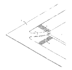
Referring now to Figure 2 of the drawings, more details of one of the comer arrangements
shown in Figure 1 is illustrated. It can be seen that the thickness of the material of leadframe
15 1 and finger 4 is less than that of carrier 2. A slight buckling or flexing of finger 4 is apparent
and this has resulted, as has been previously described, because of the equal and opposite
retentive forces exerted by the pair of fingers, for example fingers 4 and 5, on the carrier.
Finger 4 can engage or abut carrier 2 at any height within the thickness of the carrier. However
it has been found for best m~tçhin~ to have the finger close to the top edge of carrier 2, as is
20 shown. Finger 4 may also be appropriately shaped or notched, as shown by notch 9 in the end
of finger 4, in order to accommodate the shape of the corner of carrier 2, thereby more firmly
eng~ing the carrier and minimi7.ing accidental movement or slippage of the end of the finger
with respect to the carrier. Figure 2 is representative of any one of the corner arrangements. As
has been previously described, the leads 3 shown are only representative of the number of leads
25 which can be accommodated.
CA9-96-008 1 1
21 8747?
Referring now to Figure 3 of the drawings which shows in more detail one of the
representative corners of the structure illustrated in Figure 1 and is the underside of carrier 2 or
the reverse side of what is shown in Figure 2. Finger 4 is shown abutting against the corner of
carrier 2 and effectively supporting the carrier in combination with the other fingers as
5 previously described. Also, as a result of the action of the fingers and in particular Finger 4 as
shown, the ends of leads 3 are propclly positioned over contact pads 8 on carrier 2. Thus, when
carrier 2 is mounted within the resilient carrier positioning means comprising the various fingers
4, 5, 6 and 7 in the preferred embodiment of the invention, it can be seen that carrier 2 is now
properly positioned for attaching the ends of leads 3 onto the contact pads 8. As is also shown
10 in Figures 1 and 2, Figure 3 shows finger 4 as being slightly flexed or bowed. Once this
combination is placed into a furnace for reflow of the material of pads 8, any mi~m~tch in
lell~ lure coefficient between the leadframe 1 and carrier 2 is compensated for by the fingers
4, 5, 6 and 7 and the ends of leads 3 remain effectively properly positioned on contacts 8 as
previously described.
It is apparent that it is not necessary for the resilient carrier positioning means to be
positioned at the corners of carrier 2. It may very well be that the positioning means could be
located along the edges of the carrier. However, it is preferable that the positioning means be
employed as pairs so that each one exerts uniform and opposite force in order to cancel out and
20 prevent any movement of the carrier with respect to the leadframe and between the ends of leads
3 and contact pads 8.
It should be understood that the foregoing description is only illustrative of a preferred
embodiment of the invention. Various alternatives and modifications can be devised by those
25 sl~lled in the art without departing from the intended invention. Thus, the present invention is
CA9-96-008 12
21 87477
intended to embrace all such alternatives, modifications and variations which fall within the
scope of the appended claims.
CA9-96-008 13