Note : Les descriptions sont présentées dans la langue officielle dans laquelle elles ont été soumises.
2190884
A Technique for Manufacturing Integrated Optics Devices
Field of The Invention
This invention relates generally to the Integrated Optic Devices and particularly
manufacturing of hybrid integrated circuits made of different materials.
s Background of the invention.
Optical signals are used for tr~n.cmi~.cion of information by means of optical fibers and
are processed by optical devices in optics domain. Integrated optical (IO) devices are
used for processing optical signals. The basis of integrated optic (IO) devices are optical
waveguides that can guide the light. According to the laws of nature, light tends to stay
prop~ting in the higher refractive index region of the propagation media. This is the
o~el~lhlg principle of optical waveguides. An optical waveguide consists of at least two
regions called core and cl~d-lin~ The light is guided in the core region the effective
refractive index of which is slightly larger than the refractive index of the cl~d~ling~
Optical waveguides are in the forrn of 1) Slab waveguides, in which the core is
sandwiched between two cl~d-~in~c above and below (see for example Fig. 1); 2) Channel
waveguides, in which the core is surrounded by the cl;~d-1inf~ on four sides 3) Ridged
waveguide, which is similar to the channel waveguide but the core is surrounded by air
on three sides. Optical waveguides and devices are described, for example, in "Glass
Integrated Optics": Ed. by S. I. Najafi, (Artech House, 92) and in "Guided-Wave
20 Optoelectronic " Ed. by Tamir et al (Plenum Press, 1995), which are incorporated here as
references.
Channel waveguides are normally used in IO devices. Fabrication of a channel
waveguide comprises steps of evaporation, photolithography, and etching or diffusion.
For example, to make a ridge or channel waveguide in a semiconductor substrate, one
2s has to first make a mask; then deposit a layer of m~Cl!ing material on the substrate; then
coat this layer with a photoresist material; use photolithography to define the channel on
the mask; etch the mask to define the channel in the mask; and etch the substrate to
achieve a waveguide. Costly equipment such as evaporators~ reactive ion etchers, mask
aligners and so on are needed. These processes are also very sensitive and the samples
30 must be handled very carefully in order to yield a functional device. Moreover devices
made by these methods can show a high optical loss due either to the rough wall surface
or to intrinsic loss of the material. Furthermore, it is very difficult to etch or diffuse in
some materials to make integrated optics devices.
One sllccç~ful approach for making low-cost channel waveguides is to use the
3s photosensitivity effect in photosensitive materials such as sol-gel glasses. In this method
the refractive index of the photosensitive material is increased by exposure to ultra violet
- 2 1 90~84
- (W) radiation. This method is described in reference [S] for manufacturing silica-based
waveguides using sol-gel. However, fabrication of channel waveguides in other materials
is still very costly and time consuming. Moreover, making channel waveguides in some
materials, such as PLZT, is very difficult because it is hard to etch them.
5 Therefore, there is a need in the art for a simpler fabrication technique with lower
fabrication cost.
It is an object of this invention to provide a cost effective fabrication method for making
channel waveguides on any substrate material using photosensitive materials such as sol-
gel glasses.
o Summary of the invention
The present invention provides a technique to make channel waveguides on variousmaterials using photosensitive materials such as sol-gel glasses. According to the present
invention, there is provide a method for making optical waveguide devices comprising
steps of
5 a) cleaning a substrate, having refractive index nl, by means of a cleaning agent;
b) placing a slab layer (12) on the substrate, said slab layer having refractive index n2
higher than refractive index of said substrate nl; and
c) placing a layer (13) of a photosensitive material, such as sol-gel glass; having
refractive index n3 lower than refractive index of said slab layer n2; and
20 d) pre-baking the said structure in section c; and
e) placing a photolithography mask on top of the photosensitive material, having a
window opening; and
f) exposing the mask to ultra violet (UV) radiation so that W can penetrate through the
opening window into the photosensitive material; and
2s g) removing the mask.
The refractive index of the photosensitive material, 13, under the opening window of the
mask, is increased after said step (f). An increase in the refractive index of the said area
increases the effective refractive index of the said slab 12 and therefore a channel
waveguide is formed in the said slab layer under this area.
30 This technique requires fewer fabrication steps and does not use expensive equipment,
said in the introduction. The method facilitate to fabricate low-cost, low-loss and robust
integrated optic devices from both semiconductors and dielectric materials or any
material that one desires to make a channel waveguide. In the following, a detailed
description of method is described fully for a glass substrate. One can use the same
35 method for other substrate materials.
- 2 1 90884
- Brief Description of Drawings:
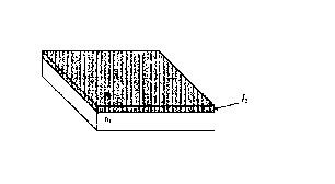
Fig. 1 is a view in perspective of one embodiment of an optical slab layer on a substrate
according to the present invention.
Fig. 2. is a view in perspective of one embodiment of the slab in Fig. 1 with a thin sol-gel
film deposited on its top according to the present invention.
Fig. 3 is a view in perspective of one embodiment of the structure in Fig. 2 of the present
o invention, covered by a contact mask, having a window open, exposing with an ultra
violet light, according to the present invention.
Fig. 4 is a lateral cross section view of the optical waveguide made according to the
present invention. Also there is shown the guided mode .
Fig. 5 is a view of one embodiment of an optical waveguide grating device.
Fig. 6. is a view of one embodiment of an optical waveguide grating device, according to
the present invention.
Detailed Description:
The structure, its one embodiment is shown in Fig. 1 and is herein referred to as the
sample. In Fig. 1 there is shown an embodiment of the sample that consists of a substrate
and a slab layer, having refractive index n2, equal or larger than substrate's refractive
index n,. Substrate and slab can be selected from various materials. The slab should be
thick enough such that light cannot be guided in the slab itself in a pure optical mode.
In Fig. 2 there is shown an embodiment of the sample that is deposited with a thin film of
photosensitive material having refractive index n3 lower than the refractive index of the
slab n2. Depending on the photosensitive material, the sample is pre-baked.
In Fig. 3 there is shown an embodiment of the sample that is covered by a
photolithography mask, having an opening corresponding to the layout of the designated
optical circuit. Also shown in Fig. 3 is the exposure of the sample to ultraviolet light
through an opening in a photolithography mask to increase the refractive index of the
thin film where it is desired to have a channel waveguide in slab layer. The mask is
removed after the exposure and the sample is post-baked.
In Fig 4. there is shown a lateral embodiment of the channel waveguide is made by the
said fabrication method. Shown also in Fig. 4 is the shape of the guided optical mode
2 1 90~84
- under the photosensitive area, refractive index of which has been increased by the said
ultraviolet exposure.
In a first embodiment of the sample shown in Fig. 1, 2, 3, and 4, the substrate is made of
glass. The slab can be part of the ~ub~ le or separately deposited on the substrate. To
5 make a slab on a glass substrate one can employ ion exchange to produce a layer of slab
with a refractive index n2 higher than the ~ubsll~le glass nl. The ion exchanged process
has been described in reference 2. The deposition of photosensitive sol-gel can be done
either by spin- or by dip-coating as explained in reference 5. The sample is pre-baked to
promote solvent evaporation and to harden the deposited film. The film contains a
10 monomer that polymerizes when it is exposed to ultraviolet light, thus increasing locally
the refractive index such that n4>n3. The sample is therefore exposed to ultraviolet light.
Finally, the sample is post-baked to stabilize the film. The increase in the refractive index
of the sol-gel thin film augments the effective index in the slab layer and produces a
channel waveguide.
In another embodiment of the sample shown in Fig. 1, 2, 3, and 4, the substrate is made
of semiconductor, electro-optic material or any other desirable material, and the slab is
made from the same material as substrate or any other material that one desires to make a
channel waveguide device from. The photosensitive layer is sol-gel glass or other
20 photosensitive material.
Different integrated optic devices can be made with similar processes according to the
present invention. Optical grating-~si~te~ devices are important constituents ofintegrated optic devices. In Fig. 5 there is shown one embodiment of a sample according
25 to the present invention. The embodiment comprises a substrate, a slab layer and a
grating structure in the slab; said gratings being defined by the Bragg resonant equation
which is:
2N (1)
where A is the period of the gratings, ~ is wavelength of the intended o~ aling optical
30 signal, and N is the effective index of the channel waveguide in Fig. 5. A method for
making the grating waveguide is described in the US patent by S. I. Najafi et al (1992)
which is incorporated here as a reference. A mask with an straight opening,
corresponding to an straight waveguide layout, is placed perpendicularly over the sample
with grating in Fig. S; the sample is exposed with a UV radiation. Therefore a straight
35 channel waveguide with grating is formed. The said gating device might be used as an
optical filter. In Fig. 6 there is shown a cross section view of one embodiment of the
sample with a grating.
2 1 90884
References:
1. S. I. Najafi, K. O. Hill, J. F. Curri, "Optical waveguide device and method for making such
device," United States Patent, Patent number, 5,080,503, Date of Patent, Jan. 14, 1992.
5 2. "Introduction to Glass Integrated Optics", Editor: Najafi, Publisher: Artech House, Boston,
1992.
3. "Guided-Wave Optoelectronics," Edited by T. Tamir, G. Griffel, and H. L. Bertoni., (Plemlm
Press, New York), 1995.
4. G. Hewa~ o. H. Hatami-Hanza, and P.L. Chu, "Wavelength-Flattened Three Core
Optical Coupler Power Splitters in Ion-Fx~h~n~ed Glass," in "Guided-Wave
Optoelectronics", Edited by T. Tamir, G. Griffel, and H. L. Bertoni,, (Plenum Press, New
York), PP.155-166, 1995.
5. C.Y.Li, J.Chisham, M.P,Andrews, S.I.Najafi, J.D.~r~n~ie, and N.Pey~h~lnb~rian, "Sol-~el
-o,, ~ d optical coupler by ultraviolet light i~ .1i..g7" ~lectron. Lett. 31 (4), 1995, pp.
271-272.
6. Procee-ling~ of the conre ~l~ce on Integrated Optics and Optoelectronics, SPIE vol. CR45,
1993.
7. Wang, S. Honkanen, S. I. Najafi, and A. Tervonen, "Loss characteristics of pUlasSi~ and
silver double-ion-eYrh ~nged glass waveguides," J. Appl. Phys. 74 (3), 1993, pp. 1529-1533.
20 8. P. Coudray, J. Chisham, M. P. Andrews, and S. I. Najafi, "UV-light i.llplh,l~d sol-gel silica
glass low loss waveguides for use at 1.55 mm," Opfical Engineering in press.