Note : Les descriptions sont présentées dans la langue officielle dans laquelle elles ont été soumises.
- ~ 2t 93269
TITLE OF T~E INVENTION
NPC Inverter Control System
R~Kr-~ouND OF TEE INVENTION
l.Field of the Invention
The present invention relates to an NPC (Neutral
Point Clamped)inverter control system to convert DC
voltage having neutral point potential into AC voltage
using the PWM control and more particularly to an NPC
inverter control system with the ;mproved control
characteri~tic by Yu~ essing the fluctuation of neutral
point potential.
2.Description of the Related Art
An NPC inverter i8 to convert DC voltage having
neutral point into AC voltage, and variouY systems are so
far developed and put to practical use. As disclosed in
the J~p-nese Patent Application (TOKU-RAI-EEI) No. 5-
268773 a-~ a pul~e width modulation control method of this
type of NPC inverter, this applicant proposed a FWM
inverter control method without uncontrollable region
which secure~ the minimum pulse width of output voltage of
an NPC inverter and outputs smooth sine wave voltage in a
full output voltage region of line voltage.
~ he outline of the control method laid open in the
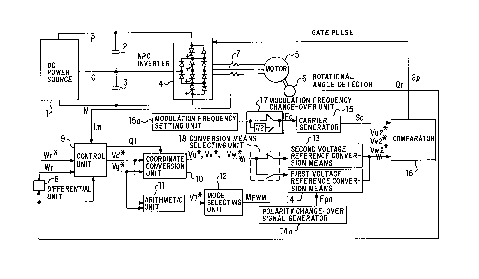
patent journal described above is shown in FIG.10 and its
Qssential point~ will be briefly described. A DC power
~ource 1 output~ DC voltage having a neutral point C
21 9326~
between termin~l~ P and N, capacitors 2 and 3 are
co~n~cted between terminals P-C and C-N and smoothed DC
voltage i8 output. The DC voltage having this neutral
point C is input to an NPC inverter 4 and is converted
into AC voltage through the pulse width modulation (PWM)
by a gate pulse Gp that is output from a comparator 16,
and i8 supplied to a motor 5.
The outline of the PWM control will be described in
the following. A control unit 9 computQs and outputs
reactive (d axis) voltage reference Vd*, active (q axis)
voltage reference Vq* and phase reference ~ 1 of primary
voltage vector from speed reference ~ r*, a rotational
angle ~ r of motor detected through a rotational angle
detector 6, a detected value of motor speed ~ r obt
through a differential unit 8 and a motor current Im
detected by a current detector 7. A coordinate conversion
unit 10 outputs voltage references Vu*, Vv*, Vw* in three
p~e~ ba.~ed on ~ 1, Vd*, Vq*. An arithmetic unit 11
obtains a vector ~um (an ~m~litude of primary voltage
reference) of Vd* and Vq* and outputq it as an amplitude
V1* of voltage reference. A mode -Qelecting unit 12
compares the voltage reference amplitude V1* with a
prescribed threshold value Vlx defined by the minimum
pulse width and outputs the mode signal M PWN of O if V1*_
Vlx and the mode signal M PWM of 1 if Vl*<Vlx and these
mode Qignal3 are input to a conver~ion mean~ ~electing
21 93269
unit 18. The conversion means selecting unit 18 operates
a first voltage reference conversion means 14 if the mode
signal
M PWM is 1 and operates a ~e~o~ voltage reference
eonversion means 13 if the mode signal M PWM is 0, and
converts three phase voltage references Vu*, Vv*, Vw*
output from the eoordinate conversion unit 10 into other
three phase voltage referQncQ Vu2*, Vv2*, Vw2* bA~e~ on
the conversion stan~d described in the following.
The first voltage reference conversion means 14
co.~v~Ls three phase voltage references Vu*, Vv*, Vw* into
Vu2*, Vv2*, Vw2* based on the following equations
aeeording to polarity ehange-over fre~uency Fpn that is
given by a polarity change-over frequency setting unit 12a.
Equations 1
Vu2* = Vu*+Vb
Vv2* = Vv*+Vb
Vw2* = Vw*+Vb
where, +Vb is set up at least more than 2 times of a
prescribed value defined according to the minimum pulse
width and is a predete~minQd bias value given in
positive/negative polarity basQd on a fixed polarity
change-over frequeney Fpn that is given by the polarity
change-over frequency generator 14a.
The second voltage reference conversion means 13
convert-~ thrQe phasQ voltage references Vu*, Vv*, Vw* into
2 1 9326~
Vu2*, Vv2*, Vw2* based on the following equations:
If U-phase voltage reference Vu* is O<Vu*<Vmin:
Equations 2
Vu2* = Vmin
Vv2* = Vv* - Vu* + Vmin
Vw2* = Vw* - Vu* + Vmin
If U-phase voltage refQrQnce Vu* is -Vmin<Vu*<0:
Equations 3
Vu2* = -Vmin
Vv2* = Vv* - Vu* - Vmin
Vv2* = Vw* - Vu* - Vmin
where Vmin i8 a predetermined voltage defined
according to the minimum pulse width.
If either V-phase voltagQ reference Vv* or W-pha~e
voltage reference Vw* is -Vmin<V*<0, it i8 also converted
likewise the above conversion equation.
When three phase voltage references Vu*, Vv*. Vw* are
all V*<-min or Vmin <V*, the three phase voltage
references are directly output as they are as shown by the
following equations:
Equations 4
Vu2* = Vu*
Vv2* = Vv*
Vw2* = Vw*
The voltage references Vu2*, Vv2*, Vw2* converted a~
described above are input to the comparator 16 together
2 1 9326~
with a triangular wave carrier Sc that is given from the
carrier generator 15 and based on its size, gate pulse Gp
i8 output to perform the pul~e width modulation and thus,
NPC inverter 4 is PWM controlled.
Accordingly, if the voltage reference amplitude V1* i8
smaller than a threshold value Vlx, the predetermined bias
is added to or ~ubtracted from voltage references in
respective phases by first voltage reference conversion
meansl4 and NPC inverter 4 outputs line voltages near a
zero-crossing corresponA; ng to the voltage references Vu*,
Vv*, Vw* while a~suring the minimum pulse width. Further,
when the amplitude of voltage reference Vl* is more than
the threshold value Vlx, if an absolute value of the
voltage reference in any one of phases i~ ~maller than
Vmin,the voltage reference in that phase is fixed at Vmin
of that polarity by second voltage reference conversion
means 13 and the voltage references in other two phases
are corrected 80 that line voltage does not change, and
NPC inverter 4 outputs line voltage corresponding to the
voltage reference~ Vu*, Vv*, Vw* while as~uring the
minimum pul-qe width.
An NPC inverter has to operate while maint~i ni ng the
neutral point potential at a constant level but has a
characteristic that it is subject to the effect of load
current and neutral point potential fluctuates at
frequency as high as 3 times of output frequency. This
21 93269
fluctuation of the neutral point potential is attributable
to the fact that a period when two phases of voltage
reference given in sine wave become po~itive and a period
when it becomes negative are taken place 3 times
alternately in one cycle. That is, when two r~e~ are
positi~e, load currents in these two phases flow from the
positi~e side P of DC power source 1 to neutral point C
and when they are negative, the load ~u~ellts flow to the
negative side N of DC power source 1 from neutral point C
and thus, the neutral point potential fluctuates.
Quantity of this fluctuation of neutral point potential
increases with the increase of load current and decreases
according to the increase of frequency.
When first voltage reference con~ersion means 14 is
selected, polarities of voltage references of all phases
are changed over to positive/negatiYe pole by polarity
change-over frequency Fpn and therefore, 8witch; ng
frequency will increa~e at a rate of once per one cycle
of chan~c o~r cycle. Further, as polarities of all
three phase ~oltage references become uniform, fluctuating
frequency of neutral point potential does not become 3
times of output frequency but b9c -.~ equal to polarity
chan~e-over frequency Fpn. Accordingly, if Fpn is
increased, an effect to suppress fluctuation of neutral
point potential i9 obtained. However, there is such a
problem that when polarity change-o~er frequencY Fpn
21 93~69
inereaqes, -qwitch~ng frequency increases and power 1088
due to 8wit~hi ng also inerease-q. In addition, there waQ
alqo quch a problem that when amplitude Vl* of voltage
referenee i8 near threshold value Vlx, the change-orer
between first and second voltage reference conversion
mQans 14 and 13 is taken plaee frequently and as a re_ult,
8witchi ng f e~u~cy inereases.
Another type of col-ve,.tional NPC inverter sy~tem iq
shown in FIG.ll. In this figure, a DC power soureé 20
i~ ~o~nseted in series with a eonverter 20c to get
positive side DC voltage Vdp from an AC power -qource 20a
and a eonverter 20d to get negative Qide DC voltage Vdn
from an AC power souree 20b, and outputs smoothed DC
voltage Vdpn (=Vdp+Vdn) between PN through an LC filter
that i8 eomposed of reaetors 20e, 20f and eapaeitorQ 21,22.
This DC voltage Vdpn having a neutral point C i-q converted
into desired AC voltage by an NPC inverter 23 and -qupplied
to load 25 as three-phaQe AC current~ Iu, Iv, Iw. These
three- pha~e AC currents Iu, Iv, Iw are detected a-q
foo~haC~ currents Iuf, Irf, Iwf by a current transformer
24 and converted into orthogonal eoordinate signal_ of
aetive eurrent eomponent Iqf and reaetive current
eomponent Idf in a conrer~ion unit (three-pha~e to two-
phase conversion) 26. This aetive eurrent component Iqf
and reaetive current component Idf are compared with the
aetire eurrent referenee Iqr and the reactive current
2~93269
reference Idr, respectively in a current controller 27 and
orthogonal coordinate signals of active voltage reference
Egr and reactive voltage reference Edr are output 80 as
to reduce respective current deviations. These orthogonal
coordinate signals Eqr, Edr are converted into three-phase
AC voltage references Vu*, Vv*, Vw* in a converter (two-
phase to three-phase conversion) 28. In a comparator 30,
thesQ three-phase AC voltage references Vu*, Vv*, Vw* are
compared with positive and negative ~ide carriers that are
output from a carrier generator 29 and output as gate
pulse GP. Inverter 23 is pulse width modulation (PWM)
controlled by this gate pulse GP, 80 that DC voltages Vdpn
between PN are converted to AC voltages corres~o~di n~ to
the AC voltage references Vu*, Vv*, Vw*, and the active
current component and the reactive current component of
the three-phase AC currents Iu, Iv, Iw are controlled to
become values corresponding to the active current
reference Iqr and the reactive current reference Idr.
Further, the positive and negative qide DC voltages
Vdp, Vdn are detected as voltage feedback Vdpf, Vdnf by
voltage detectorq 31, 32, its differential voltage ~ Vd
is added to AC voltage references Vu*, Vv*, Vw* and AC
-output voltage of inverter 23 i-q -qo controlled that thiq
differential voltage i8 made zero by the corrected AC
voltage references Vu2*, Vv2*, Vw2*. As a result, if a
difference is generated between the positive and negative
` 21 q3269
side DC voltagQs Vdp, Vdn of DC power qource 20, the
neutral point potential fluctuates to generate a
differential voltage ~ Vd and the AC voltage references
Vu2*, Vv2*, Vw2* that are the corrected AC voltage
references Vu*, Vv*, Vw*, are given to a comparator 30 80
as to make the differential voltage ~ Vd zero. Thus, NPC
in~erter 23 is so controlled that a difference is
generated bQt~een the positive and negative side powers to
suppress fluctuation of the neutral point potential.
If, for in~tance, the positive side DC voltage Vdp
become-~ larger than the negative side DC voltage Vdn, the
differential voltage ~ Vd is added to bias the AC voltage
references Vu*, Vv*, V~* in the positive direction, it is
so corrected and controlled that power supplied from the
positive side DC ~oltage Vdp increases and power supplied
from the negative side DC voltage Vdn decrea~es and a~ a
result, the fluctuation of the neutral point potential is
~p es~ed.
~ owever, on a c~ ntional NPC converter system
described above, DC voltage may be o~cillated by reso~nce
frequency of an LC filter, that is composed of reactors
20e, 20f and capacitors 21, 22, resulting from fluctuation
in loads and/or output frequency. Converters 20c and 20d
are equipped with a voltage control ~ystem (not shown),
respectively, for controlling DC voltage and DC voltage
may oscillate in connection with the voltage control
21 9326q
response and the resonance frequency. Further, as the
differential voltage ~ Vd is not detected if po~itive
current voltage Vdp and negative current voltage Vdn
fluctuate while they are in accord with each other, the
fluctuation of DC voltagQ cannot be suppressed by the
correction control described above. Further, if positive
side DC voltage Vdp and negative side DC voltage Vdn
fluctuate in the same phase by the fluctuation of thQ
active current component of AC current output from
inverter 23, the differential voltage ~ Vd becomes zero
and therefore, the fluctuation of DC voltage cannot be
suppressed.
As a result, on a conven~;o~ NPC in~erter system it
is inevitable to cope with fluctuation of DC voltage by
delaying voltage control responses of the converters and
it was not able to suppres~ fluctuation of DC voltage
sufficiently. Therefore, when a motor to drive a rolling
mill i8 applied a~ a load, a control response to
fluctuation of the load becomes slow, the control output
torqye is fluctuated, the rolling action i~ infl~l~nce~ and
the product quality may be adversely affected.
A co-.ve.,tional NPC inverter that iQ u~ed in
foregoing NPC inverter system is shown in FIG.12. In
this figure, a converter 40 obtains DC voltage from an AC
power ~ource (not shown) and output-Q it via a reactor 41
and outputs DC voltage having a neutral point C ~moothed
by capacitors 42, 43 connected in series between P and N.
There are switching elements S1-S4(Su1-Su4,Sv1-Sv4, Sw1-
Sw4) composed of diodes connected in reverse parallel via
fuses 44a - 44f connected in series for each phase between
PN, and potential at one of 3 levels of the positive pole
P, negative pole N and neutral point C of DC voltage is
output to respective AC output terminals U, V, W in the
shape of pulse, pulse width modulated AC voltage is output
and AC power of good quality is supplied to a load 45.
When switching elements S1 and S2 of the positive side
arm are simultaneously turned ON, the potential of the
positive pole P is output, when switching elements S3 and
S4 of the negative side arm are simultaneously turned ON,
the potential of the negative pole N is output, and when
both switching elements S1 and S4 are turned OFF and
switching elements S2 and S3 are simultaneously turned ON,
the potential at neutral point C is output through either
a neutral point clamped diode D1 or D2(Du1 or Du2,Dv1 or
Dv2,Dw1 or Dw2). Further, when the positive AC voltage
is output, switching element S2 is turned ON and switching
element S1 is turned ON/OFF. When the negative AC voltage
is output, switching element S3 is turned ON and switching
element S4 is turned ON/OFF. Further, switching elements
S1,S3 and S2, S4 are turned ON/OFF complimentarily but
never turned ON simultaneously. This switching control
operation is well know and therefore, its detailed
11
2 1 93269
-
explanation will be omitted.
On such an NPC inverter _ystem, when QWit~h i ng element
S2 is in the ON -qtate and switchi ng element-q S1 and S3 are
turned ON/OFF complimentarily to output the positive AC
voltage, if 8witchi ng element S1 i8 not t~rneA OFF when it
should be turned OFF and kept in the ON Qtate, and
~wi~chi ng element S3 is t~r~e~ ON or ~witC,hi ng element S1
is t~rn6~ ON and switrh; n~ element S3 i~ kept in the ON
state for somQ rQason although it should normally be
turned OFF, the ~hort-circuit current flows out of
c~p~ritor 42 through neutral point clamped diode D2. In
~uch a case, fuse 44a (or 44c,44e)is burnt down to
eve..t switchi"g elements S1 - S3 from being damaged. If
switching element S2 is turned ON when 8witch; n~ elements
S3, S4 are turned ON simultaneouqly, the short-circuit
current flowq out of c~r~citor 43 through neutral point
clamped diode D1, fuse 44b (or 44d,44f)iq burnt down to
prevent s~itch;ng elementQ S2 - S4 from being damaged and
thus, the ~Yp~n~ion of trouble is prevented.
Fuses for proteeting an NPC inverter system from the
short-circuit described above are not a little heated by
the cu~ ellt flowing during the operation, exposed to a
high temperature environment for an exten~ period,
grA~ y deteriorated and tend to be ea~ily burnt down
and in order to qecure reliability of protective
characteri~tic, nee~e~ to be replaced periodically (for
- 21 93269
in-Qtance, every 1 - 2 years) and are therefore
uneconomical. In recent yearQ, NPC in~erterQ in high-
tension large capacity of Qeveral kV DC voltage are put to
practical use with the development of semiro~ ctor
deYices. As a re_ult, high-tension protective fuses
become necessary and coupled ~ith the problem described
above, an economical and highly reliable _hort-circuit
protection without using fuse i_ desired.
sr~uM~Y OF THE Ihv~..lON
The present invention i_ made in vie~ of the problems
deQcribed above and it i8 an object to provide an NPC
inverter control _yQtem c~pahle of effectively &u~ eQQing
fluctuation of neutral point potential ~ithout incr~asi ng
Q~it~hing frequency.
It iQ another object of the presQnt invention to
provide an NPC inverter control syQtem with the improved
control characteriQtic by correcting and controlling
active current component of AC output current by detecting
fluctuation of DC voltage, -Quppressing o~cillAtion of DC
voltage by LC reso~ance of a DC power source.
It is more another object of the present invention
to provide an economical and highly reliable NPC inverter
capable of protecting _witchi ng elementQ from Qhort-
circuit current without u~ing fu_eQ and preventing the
expan~ion of troubles.
According to thi_ invention there is provided
13
- 21 93269
an NPC inverter control system characterized in that it is
equipped with a DC power source to output DC voltage
having a neutral point, an NPC inverter to convert the DC
voltage into AC voltage in three phases through a PWM
control, a mode selecting unit to ~ci~q a first and a
second PWM modes by comparing amplitude of voltage
reference with a prescribed value that is defined by the
minimum pulse width, a first voltage reference conversion
means to add a prescribed bias value at which the polarity
rh~ngos to positive/nQgative ~ithin a fixed period to
secure the minimum pulse width to voltage references in
respective phases in a first PWM mode, a second voltage
reference conversion mean~ to fix the voltage reference in
one phase by a value that secures the minimum pulse width
when voltage reference in one phase is smaller than a
prescribed value that is defined by the minimum pulse
width in a second PWM mode and correct voltage
references of other two phases 80 as to make line
voltage to a value correspon~; ng to the voltage reference,
and a modulation frequency change-over means to lower PWM
control dulation frequency in the first PWM mode and
to ~u~ e88 power 1088 by the swit~h~ ng in the first PWM
mode.
Further, according to this invention there i~
provided an NPC inverter control ~ystem characterized in
that it is equipped with a DC power source to output DC
14
- 2 1 93269
voltage having a neutral point dividing it into positive
and negative side voltages through an LC filter, NPC
inverters to convert the DC voltages into AC voltageQ of
desired frequency and ~upply AC current to load~, a
current control means to control the NPC inverters 80 as
to reduce current deviations by comparing active current
reference and reactive current reference with detected
values of active current component and reactive current
component, and a correcting means to output a fluctuating
component of the DC voltage in the region above a
prescribed frequency as a correction signal and correct
the active current reference 80 as to suppreqs fluctuation
of the DC voltage by this correction 8i gnal,
Further, according to this invention there is
provided an NPC inverter characterized in that it is
equipped with a DC power source which, with the connecting
point of two sets of serie;s co~n~rted c~r~r~tors used as a
neutral point, outputs DC voltage, an NPC inverter unit,
with the positivQ and negative poles of the DC power
source and the neutral point ~onnocted, convert-~ the DC
voltage into AC voltage, a first and a second branch
circuits each of which is a series circuit composed of a
reactor and a 8witrh i ng element provided.between the
positive and negative sides of the DC power source and the
neutral point, and when short-circuit current of the ~PC
inverter unit i~ detected, the 8witch; ng elements of the
21 93269
first and the second branch circuits are turned ON, thus
protecting the NPC inverter unit.
BRIEF DESCRIPTION OF THE DRAWINGS
FIG.1 is a bloek diagram showing an ~mhodiment of an
NPC inverter control system of the present invention;
FIG.2 is a voltage ~aveform diagram for expl~i ni ng the
action of a second voltage reference conversion means 13
in the embodiment sho~n in FIG. 1;
FIG.3 i8 a voltage waveform diagram for expl ai ni n~ the
aetion of a first voltage referenee ~o.~v~ ~ion mQans 14 in
the embodiment shown in FIG. 1;
FIG.4 i9 a block diagram of an embo iment of an
another NPC inverter system o~ the prQsent invention;
FIG.5(a) is a bloek diagram showing the eharaeteristie
of a high-pass filter; (b) is a block diagram of the
essential portions of an embodiment of an NPC inverter
system of the present invention; (c) is a diagram showing
the gain characteristic of arithmetic units;
FIG.6 is a block diagram showing an another
embodiment of an another NPC inverter system of the
present invention;
FIG.7 is a block diagram showing an embodiment of an
NPC inverter of the present invention;
FIG.8 is a time chart for expl~i ni ng the operation of
the embodiment of Fig.7;
FIG.9 is a block diagram showing an embodiment of an
16
2 1 93269
another NPC inverter of the present invention;
FIG.10 is a block diagram showing a col-vel~tional NPC
inverter control system;
FIG.11 i9 a block diagram showing an another
co~,vantional NPC in~erter system; and
FIG. 12 is a block diagram sho~ing a co.-vQ.~tional NPC
inverter.
DE~TT~n DESCRIPTION OF T~E ~ ~K~ED EMBODIMENTS
An embodimQnt correspo~; n~ to an NPC in~erter control
systQm of the prQsQnt invention as claimed in claim 1 is
sho~n in FIG.1. In the construction sho~n in FIG.1, 17 is
a modulation frequency rh~ng~-ovQr mQans and when mode
8i~n~l M PWM givQn from mode selQcting unit 12 iq 1,
outputs setting frequency of carrier frequency sQtting
unit 15 by rs~ i ng it to 1/2 and when mode signal M PWM
iq 0, outputs setting frequency of carrier frequency
sQtting unit 15 aq it is, and changes over modulation
frequency Fc according to the mode signal 1,/0. Carrier
generator 15 generates triangular wave carrier Sc of the
modulation frequency Fc that is changed over by the
modulation f~e~uency change-over means. All other
element~ are the same as those used in a ~G..v~.tional NPC
invertQr control system (FIG.10).
In the construction described above, ~hen amplitude
V1* of voltage reference that iq output from arithmetic
unit 11 is less than prescribed threshold value Vlx
21 93269
defined by the minimum pul3e width (Vl*~Vlx), mode signal
M PWM of 1 i3 output from mode selecting unit 12 and when
it iL~ more than threshold value Vlx (V1*2Vlx), mode
Qignal M PWM of 0 is output from mode selQcting unit 12.
When mode signal M PWM i8 1, the function of firQt voltage
refQrence converQion means 14 is validated by conver.~ion
means selecting unit 18 and at the same time, modulation
frequency Fc i-Q re~ce~ to 1/2 of setting frequency of
carrier f ~u~-cy setting unit 15a. Further, when mode
~ign~l M PWM is 0, the function of 9econ~ voltage
reference con~ersion means 13 is validatQd and voltage
refQrQnces Vu*, Vv*, Vw* in reQpective phases that are
o~u~ from coordinate conversion unit 10 are converted to
Vu2*, V~2*, Vw2*.
When the function of first voltage refQrence
conversion means 14 iQ validated, bias voltage in square
wave of a period T1 defined by polarity change-over
frequency Fpn i~ added to voltage refQrences in respective
~h~ eQ Vu* ~ Vv*, Vw* as shown in FIG. 2, and converted
voltage references Vu2*, Vv2*, Vw2* are changed one ti m~
to positive/negative in period T1. Period T0 of carrier
Sc is ~c~ according to modulation frequency Fc and
becomes 2 times of a normal modulation period~ Shown in
FIG. 2 is an example wherein polarity change-over
frequency Fpn was set at 1/5 of modulation frequency Fc.
When the function of 8~Co~ voltage referQncQ convQrsion
18
21 93269
means 13 is validated, the period T0 of carrier Sc is
ehanged over to the norr~l modulation period that is
decided aceording to setting frequeney of carrier
f e~u3.~ey setting unit 15a and suppressed ~imilarly as
before.
In this ~mhodiment, when mode signal M PWM is 1, a
preseribed bias is added to or subtracted from voltage
references as deseribed above and NPC inverter 4 outputs
~mooth sine wave line voltages corresron~; n~ to voltage
references Vu*, Vv*, Vw* while assuring the minimum pul~e
width near the zero-crossing of-the voltage reference~.
In this ea~e, modulation frequency i~ r~ to 1/2 of
the normal level and even when polarity ehange-over
frequeney Fpn is set at a large level, it becomes lower
than the normal modulation frequency Fe. As output
frequeney is generally lower in a region wherein voltage
references are low, a harmonic cont~i ni n~ rate is also low
and the control efficiency does not drop. Accordingly,
even when polarity change-over frequeney Fpn is set at a
higher level, power 108-~ due to 8witchi n~ does not beeome
higher than a normal level and fluctuation of the neutral
point potential can be effieiently suppressed.
Further, mode ~eleeting unit 12 ~hown in FIG. 1 is in
sueh strueture that it has a hysteresis eharacteristie
when changing over a mode by ~etting mode ~ignal M PWM at
1 when amplitude of voltage referenee V1* i~ less than a
19
- 2 t 932~9
prescribed threshold ~alve Vlx (Vl*<Vlx) that is ~?Ci ~G~
according to the minimum pulse width and setting mode
signal M P~M at 0 when a little value ~ V is added to Vlx
(V1*2Vlx+~ V) and when the NPC inverter is operated at
the amplitude of voltage reference V1* near a prescribed
value Vlx defined according to the minimum pulse width,
and it is possible to ~ t the generation of chattering
and suppress increase of switching frequency resulting
from the mode change-over.
According to the above mentioned present in~ention,
it is pos~ible to provide an NPC inverter control system
capable of ~uppressing fluctuation of neutral point
potential without increa~ing switchin~ frequency in a low
voltage reqion wherein amplitudes of voltage refQrences
are 1Q88 than a prescribed value defined according to
minimum pul-~e width.
An embodiment of an another NPC inverter ~ystem of
the prQ9QIlt invQntion i9 shown in FIG.4.
In the construction of the NPC inverter system shown
in FIG.4, 33 is an active current correction unit to get a
correcting signal Iqc from the detQcted value of positive
side DC voltage Vdpf and that of negative side DC ~oltage
Vdnf, and is composed of an adder 34 to get an added value
(Vdpf + Vdnf) of a detected value of positive side DC
voltage Vdpf and that of negativQ side DC voltage Vdnf,
that is, DC voltage Vdpn L~..een PN of DC power QourCe 20
~0
- 21 93269
and a high-pass filter 35 to output only the high-
frequency region as correction signal Iqc by removing the
low-frequeney region ineluding DC components below a
preseribed frequeney of fluetuating eomponents when DC
voltage Vdpn between PN fluctuates. 36 is an adder to add
eorreetion signal Iqe to aetive eurrent reference Iqr.
All other-Q are in the same construction as in a
co.,v~l.tional NPC inverter systQm
In the construction deseribed above, NPC inverter
systQm 23 outputs three-phase AC ~u~ e--ts Iu, Iv, Iw
similar to a eonventional inverter system based on active
current reference Iqr and reactive current reference Idr
and if a differenee i8 generated between positivQ and
negative side DC voltages Vdp and Vdn of DC power ~ource
20 and a differential voltage a Vd is detected, AC voltage
referenees Vu*, Vv*, Vw* are eorreeted and controlled ~o
as to suppress the neutral point potential to fluctuate
likewise a cG--Y~-ltional NPC inverter sy~tem
Further, in this embodiment, when DC voltage Vdpr
between PN of DC power source 20 fluctuates, eorreetion
signal Iqe of the high-frequency region with the low-
f ~e.ley region ineluding DC eomponents below a
prQseribed frequency of the fluctuated components removed
i8 output from active eurrent eorrection unit 33 and added
to aetive current reference Iqr via adder 36. As a
rQsult, if DC voltage Vdpn betweQn PN fluetuates, aetive
21
21 93Z69
current components of AC currQnts Iu, Iv, Iw that are
output from NPC inverter 23 are corrected and controlled-
80 as to suppress the voltage fluctuation. For instance,
if DC voltage Vdpn between PN changes in the increa~ing
direction, active current componQnts are corrected in the
increasing direction and if DC voltage Vdpn changQs in the
decre~ g direction, active current components are
corrected in the decreAs;ng direction and as a result,
fluctuation of DC voltage Vdpn is suppressed.
Shown in FIG.5(a) is a transfer function showing the
characteristic of high-pass filter 35, a 35a is a transfer
block to pas~ only a low-f e~ue~cy region including DC
components belo~ a frequency determinQd by a prescribed
time constant T of input 9;~nAl ~ 35b is a subtracter to
subtract the low-frequency region of the input signal
passed through transfer block 35a, 35c is an amplifier to
convert the output signal of subtracter 35b to a
prescribQd level and output as correction signal Iqc.
From the construction described above, only high-frequency
components ~ith the lo~-frequency region including DC
components below a frequency that i8 determined by
prescribed time constant T removed from input signal Vdpn
(a detected value of DC voltage Vdpn bet~een PN) is output
as correction signal Iqc.
According to this ~mhodiment, when DC voltage
fluctuates ~hile resonating the reso~Ance frequency of LC
22
21 93~6Y
filter of DC power source 20 resulting rom fluctuation of
load~/output frequency, it i~ posqible to get a dumping
effect to effectively quppress DC voltage fluctuation by
properly ~etting a time constant T of high-pass filter 35a
and improve a voltage control response of a converter
operating as a DC pouer source without generating an
oscillation phenomenon. Accordingly, when a motor to
dri~e a rolling mill i8 applied as a load, fluctuations of
the control output torque of the tor as ~ell as an
effect given to the rolling action are ~u~essed and such
a problem that product quality is adversQly af$ected is
solved.
An embodiment of plural NPC inverter system of the
present invention i~ shown in FIG.6. Shown in this
embodiment is a common power ~upply system to supply DC
voltage having a neutral point C output from one DC power
source 20 to a plurality of NPC inverters 231 - 23n and
~upply ;n~.e~nt AC current to motor-q (load~) 251 - 27n.
In FIG.6, 371 - 37n are control unit-q to control NPC
invQrters 231 - 23n and motorq (loads) 251 - 25n baqed on
respectivQ active (tOrqUQ) current reference Iqr and
reactive (exciting) current reference Idr and are provided
with adders 361 - 36n to add correction ~ignal Iqc to
respective active current references Iqrl - Iqrn.
In the con~truction described above, if voltage
bet~Qen PN of the common DC po~er source fluctuates,
23
2193269
correction signal Iqc in the high-frequency region with
the lou-frequency region including DC components below a
prescribed frequency of the fluctuation components removed
i8 added from active ~u~ e~-t correction unit 33 to torque
current rQferQnces Iqrl - Iqrn and active (torque) current
componQnts of AC current output from NPC inverters 231 -
23n are corrected and controlled to suppress voltage
fluctuation betwQen PN.
In case of this ~mhodiment, NPC inverters 231 - 23n
are able to operate ~ ,ende--tly, output different
freq~ ci 98 and therefore, DC voltage may fluctuate for
the relation between respective frequency differences and
LC rs~Q~an~e frequency o DC power source 20. This DC
voltage fluctuation can be suppressed when time constant T
of high-pass filter 35 of active current correction unit
33 is set at a proper value.
Another emboAiment of an NPC inverter system of the
present invention iq sho~n in FIG.5(b). This ~mhodiment
is the same as the emboAiment shown in FIG.6 but added
with arithmetic units 381 - 38n.
These arithmetic units 381 - 38n are composed of
amplifiers of which gains change according to active
current references Iqrl - Iqrn, and output s~co~A
correction signals Iqcl - Iqcn multiplied by a gain that
decreases in proportion to increase of active current
references Iqrl - Iqrn a~ai n8t correction -~ignal Iqc
24
- 21 93269
output from active current correction unit 33. Respective
active eurrent references that are given to reQpeCtiVe
current control means are corrected by this second
correetion signal 90 as to suppress DC voltage fluetuation.
FIG.5(e) is a gain charaeteristic of arithmetic units
381 - 38n and sho~s the relation of the ehange in gain
against size (absolute value) of active current reference
Iqrl - Iqrn.
Charaeteristic C1 is to reduee a gain of arithmetie
units 381 - 38n aeeording to inerease in size (absolute
value) of aetive eurrent references Iqrl - Iqrn and makes
the gain zero at preseribed aetive eurrent reference Iqrx.
Charaeteristie C2 is to maintain a gain at a eonstant
level ~hen size (absolute value) of aetive ~u~..t
rQferenees Iqrl - Iqrn is below preseribed value Iqrx and
make it zero when Iqrx i9 e- ~ e~
Aecording to the these embodiment, when supplying AC
~u~ ~-t to motors (loads)251 - 25n by a plurality of NPC
invertQrs 231 - 23n of the eo on power supply system, it
is possible to suppress the fluctuating component of DC
voltage by light loaded NPC inverters (including no
loaded) by giving second correction signal Iqe to only NPC
invertQrs that are supplying active current comro~ent
belo~ preseribQd aetive current reference Iqrx and without
giving second correetion signal Iqc to NPC inverters that
are supplying active eurrent eomponent above preseribQd
21 93269
-
aetive current reference Iqrx. Therefore, when voltage
fluetuation is suppressed if DC ~oltage i~ oscillated by
the resonance of an LC filter of the DC power source, the
eorrection and control are carried out by NPC invQrters
that have a surplus in output eurrent without providing
8eCG~.d eorreetion signal Iqc to NPC invertQrs that are
supplying AC current to a tor (load) that has a rolling
load ~hile observing the operating statQ of every NPC
inverters and the rolling action is thus not adversely
affeeted.
In the above description, an example to obtain DC
voltage between PN of DC power source 20 by a~ ng a
deteeted value of positive side DC voltage Vdpf and a
deteeted value of negative side DC voltage Vdnf is
presented. DC voltage bQt~een PN also ean be obtAi n~
similarly using a voltage deteetor to direetly deteet DC
voltage betNeen PN.
According to the present invention, it is possible to
eorreet and eontrol aetive ~u~ ~nt components of AC output
eurrent 80 as to supprQss fluetuating voltage by detecting
fluctuating eomponent of DC voltage, to make DC voltage
stablQ by suppres~ing an oscillating phenomenon of DC
voltage resulting from LC reso~nre of DC power source and
provide an NPC inverter system with the im~roved control
charactQristic.
An embo~iment of the NPC inverter applicable to
26
21 93269
Fig.1, 4, and 6 of the pre_ent invention is shown in FIG.
7. In FIG.7, 50a, 50b are Qhort-circuit swit~hi ng
elem~ents which are turned ON in response to a -qhort-
eireuit eommand Se, 51a and 51b are reaetors qo~n^eted to
car3~-;tors 42, 43, 60 iq a eurrent transformer to detect
instantaneous eurrent flowing between neutral point C and
an inverter unit 46, 70 is a control unit to output a
~hort-circuit eomm~nd Se and a stop eommand RCB when
deteetQd eurrent Ic ~ 9-1~ a prescribed value. All
others are the samQ component elements as a cG~.~Q..tional
NPC inverter (FIG.12) and are assigned with the same
reference numQrals. Further, in this embodiment reactors
52a, 52b for l;~iting a change rate of cu~ ~nt 410wing to
s~it~-hi ng elements S1-S4 (Sul-Su4,Svl-Sv4,Swl-Sw4)
conn~eted in serie~ are provided at the P and N sides of
DC input of inverter unit 46. An NPC inverter may be in
such construction that reactors may be connected in
series to 8witchi ng elements S1 - S4 ~hich are connected
in ~eries for all pha ~e8 .
In the construction described above, the instantaneous
current flowing through neutral point C is detected by
CurrQnt transform~r 60, and _ize (an absolute value) and
polarity of this detected current Ic are constantly
monitored by control unit 70. If the short-circuit
current flows to the pOQitive qide or the negative side
8witchi ng Qlements, the positive pole or the negative
27
` 21 93269
poles detecting current Ie in size proportional to the
short-circuit current is output from current transformer
60 and if its sizQ eYe~e~ a preseribQd value, control
unit 70 outputs short-eireuit eommand Se to turn short-
cireuit switehi ng element 50a or 50b ON. At the same time,
the PWM eontrol of in~erter unit 46 i9 stopped and
8witrhi n~ elements Sl-S3 or S2-S4 in all rh~ are turned
ON. Aeeordingly, the short-eireuit current i8 brA~ChO~ to
reaetors 51a and 52a or reaetors 51b and 52b, and the
cu~ ~"t flowing to a 8~itoh; ng element in the phase
generating the short-eireuit is-shared and re~llee~ by the
8witchi ng elQments in all phasQs. As the brAnrhi ng ratio
is deeided aeeording to an induetanee ratio of reaetors
51a and 52a or reaetors 51b and 52b, it is po~siblQ to
eve,.t and proteet the switehing elements from being
damaged by ~eri~ing the induetanee ratio of reaetors ~o as
to restriet the ~hort-eireuit eurrent flowing to the
positi~e or the negati~e side switehing elements ~ithin
the allowable eurrent.
At the same time when outputting the short-eireuit
eommand Se, eontrol unit 70 also outputs the stop command
RCB to stop the operation of eon~erter 40 and therefore,
most of the short-eireuit eurrent beeomes diseharge
eurrent of aeeumulated eharge (energy) of eap~eitor 42 or
43. A-~ this discharge eurrent flow~ to the circuit of
eapaeitor 42 and reaetors 51a, 52a or the circuit of
28
- ~1 93269
capacitor 43 and reactors 51b, 52b, it becomeq an
oscillation waveform current that is decided by its
resonancQ frequency and the accumulated charge ~energy) of
~ar-c;tor 42 or 43 i8 moved to r~actors 51a and 52a or
reactors 51b and 52b as magnetic energy, the accumulated
charge of that capacitor bQcomes zero, the discharge
current becomes maYimum and the magnetic energy also
become~ maximum when voltage becomQs zero. From thi~
point of time, the discharge current generated by
~ charge of the magnetic energy continuously flows,
car-citor 42 or 43 i~ charged to the rQvQrsQ polarity, and
when the magnetic energy bQcomes zero and the current
becomes zero, short-circuit ~witchi ng element 50a or 50b
i8 turned OFF and at the samQ time, 8witchi ng element of
the inverter unit 46 kept ON is t~rne~ OFF. Further, at
this point of t me, the polarity of voltage of capa~-;tor
42 or 43 is turned to the reversed state. Accordingly,
from this point of time, the discharge current flows in
the reverse direction from ~p~ritor 42 or 43 through
neutral point clamped diode D1 or D2 (Dul or Du2, Dvl
or Dv2, Dwl or Dw2)and a diode co~n~-ted in rever~e
parallel to swit~hing element S1 or S4 in each phase of
inverter 46 and reactor 52a or 52b. In this ca~e, the
, .. .. ...
reqo~-nce frequency of the dischargQ circuit becomes a
little low, the o-~cillation current becomes long in period
with a high crest value and becomes zero after a half-
29
- 21 93269
period, and voltage at capacitor 42 or 43 i8 restored to
the original polarity.
FIG.8 shows an example of operation when a short-
eireuit trouble i9 generated at the positive side
gwitchi ng el~m~nt9 in U-phase of inverter unit 46. Now,
if the PM~ control i8 carried out as s~itch; ng elementg
Sul and Su3 are turned ON/O.~F eomplimentarily in the state
~here s~it~hi~g element Su2 is kept ON and at the point of
time tl, switching element Su3 is t~r~e~ ON with swit~
element Sul t~-~e~ OFF from the ON state and switchi ng
element Sul i-Q failed to be t~n~~ OFF and 3witehi ng - -
element Su3 i9 tl~n~A ON, the eircuit between P and C of
the DC ,~o~e~ -Qouree beeomes short-cireuited via reaetor
52a, switc~hing el~m~nts Sul, Su2, Su3 and neutral point
elamped diode Du2, and diseharge current I~ flows out of
capacitor 42 as the short-eireuit current. This discharge
current is detected as the positive polarity detecting
ent Ie by current transformer 60 If ~ize (an
absolute value) of this discharge current I~ eel-~ a
prescribed current Io, control unit 70, judging the
positive side arm to be in t'e short-circuited state from
the polarity of the diseharge current Is, output~ short-
cireuit eo.mmand Sc to turn short-cire~i tQ~ ~Wit~h~ ng
element 50a ON and suspends the ~W~. eontrol and turn
~witch~ ng element~ Sul-Su3, Svl-Sv3, Swl-Sw3 in all phase~
ON. As a result, the ~srh~rge ~u~le5~t is brAnch~ into
21 93~69
reactors 51a and 52a and flows thereto as oscillation
current and after the half period of the resonance period,
the current becomes zero. At thi-q point of time t2,
short-circuited 8wit~h; ng elQment 50a and 8Wit~h; ng
elements Sul-Su3, Svl-Sv3, Swl-Sw3 in all pha ~e8 are
turned OFF. During the period to this point of time tl -
t2, the polarity of voltage Vcl of carac;tor 42 is
6~s~1. From the time t2, by the revQrsed voltage Vcl
of cap-c;tor 42, ~;s~ha~ge current is forced to flow in
the reverse direction from capac;tor 42 via ..euLlal point
clamped diode Dul, Dvl, Dwl in all rh - ~-8 and the diode
connected in revQrse parallel with swi~ch; ng elQments Sul,
Svl, Swl and reactor 52a. As this ~;sch~ge ~u~ ent
10ws to only reactor 52a, the reso~Anc~ frequency of the
discharge circuit becomes a little low, the oscillation
current becomes long in period with a low crest value and
at the point of time t3 ater a half period, the current
becomes zero and voltage Vcl of capacitor 42 is restored
to the original polarity. In this case, the positive hal
period short-circuit current flows -qeparately to 8witch; ng
elements Sul-Su3, Svl-Sv3, Swl-S~3 and neutral point
clamped diodes Du2, Dv2, Dw2 in all phases and it becomes
thus possible to restrict the short-circuit current
10wing to the 8witchi ng elemQnts within the allowable
range, thereby protecting the 8witch; ng elements by
sQtting an inductance ratio of reactors 51a and 52a at a
31
21 ~326~
proper value.
When a short-circuit trouble is generated on the
negative ~ide 8witch; ng elements in U-phase of inverter
unit 46, the ~;.qrhArge current flo~s from cap-citor 43
through neutral point elamped diodes Dul, Dvl, D~1,
switeh;n~ elemQnt~ Su2,-Su4, Sv2-Sv4, Sw2-Sw4 and reactor
52b, the negative polarity deteetion eurrent Ie i8
deteeted from eurrent tranQformer 60 and control unit 70
G~uLs short-eircuit eommand Se to turn short-eircuited
8~itch~ ng elQment 50b ON and thus, the proteetive
operation is earried out in the same manner a~ deseribed
above.
An another embodiment of the NPC inverter o the
present invention is sho~n in FIG.9. In this embodiment,
eurrent transfo~m~rs 60u, 60v, 60w are provided to deteet
current flowing in/out of the neutral points for every U,
V and W phases of inverter unit 46 and a function is
provided to control unit 70 to detect and display a phase
generating a short-eircuit trouble from these deteeting
current Ieu, Iev, Ic~. In thi~ embodiment, if a trouble
is generated in any phase to cause a short-circuit between
P and C or N and C of DC voltage, the -qhort-cireuit
uu~ e..t flow~ to a eurrent transformer in eorrespo~; ng
.. _ .. . . .
phase and the protective operation i~ earried out similar
to that de~cribed above. Further, control unit 70
monitors the detection ~u~ent Icu, Iev, Iew,
- 21 93269
diseriminates a phase generated a -Qhort-circuit trouble
from a detection current first exceeded a prescribed
eurrent Io and from the polarity of that deteetion current,
di~er; m; nates and displays whether the short-eireuited arm
is the positive side or the negative side.
Aeeording to this omhodiment, it beeomQs possible to
easily detect a swit~h;ng element generating a short-
eircuit trouble and improve the mainta i n -h; 1 ity.
In the above embodiment, an example to perform the
proteeti~e operation of an NPC inverter by deteeting the
neutral point current is deseribed. It is also possible
to perform this operation using a eurrent deteetor to
deteet ~iseh-rge eurrent of car~eitors 42, 43. Further, a
short-eireuitQd s~i~eh;"g element i8 deseribed using an
example to operate either the positive polarity side or
the negative polarity sidQ. In sueh a case where the
circuit between P and N i~ short-cireuited, when operating
both polarity side short-eireuited 8witchi ng elementQ
using a current deteetor deseribed above, they operate
similarly and the same effeet ean be obtaine~.
Further, although an NPC inverter to obtain DC voltage
having neutral points using t~o sets of capa~c;tors
~onn~et~d in series and obtain AC voltage through PWM
eontrol of 3 level potentials is de~eribed in the above.
the proteetive technique of this invention is also
applieable to an in~erter to obtain AC ~oltage by dividing
33
- 21 93Z69
in multi-stages of DC voltage between the positive pole P
and neutral point C and bet~een the nogative pole N and
neutral point C by 2 N sets of ~ap-ritors co~n~rted in
series and through the PWM control of multi-level
potentials more than 3 level~.
According to the NPC inverter of the presont
invention, as it is pos~ible to protect -q~itching elements
~ithout using fuse~ for protecting them from short-circuit
when a short-circuit trouble is taken place on an NPC
in~erter, the necessity for periodic fuso replacement is
eliminated and it is possible to provide an NPC inverter
system with easy maintenan~e, impro~ed economical
efficiency and promoted r~liahility for short-circuit
protoction.
34