Note : Les descriptions sont présentées dans la langue officielle dans laquelle elles ont été soumises.
~ W0 96102922 2 ~ q ~ 9 6 8 r~ ./ 5 r
VARIABLE VOLTAGE PROTECTION
STRUCTURES AND METHODS FOR ~AKlNG SAME
FTFT.l) OF T~TF INVFNTION
The present invention relates generally to variable voltage protection
devices used to protect electronic circuits from u~YulL. t~ transients caused by5 lightning, e le~,LI~ ,. pulses, L~le~ u~L~ discharges, ground loop induced
transients, or inductive power surges. The present invention relates 1 ' 1
to a variable voltage protection component with a ~ "y constant
thickness for assembly in a variable voltage protection device.
BACKGROUND OF THE INVENTION
Voltage transients can induce very high currents and voltages that can
penetrate electrical devices amd damage them, either causing hardware damage
such as ~...~ .., burnout, or electronic upset such as i ~ Ioss ûr
loss of stored data. The voltage transients produce large voltage spikes with
high peak currents (i.e, over-voltage). The three basic over-voltage threats are15 LI~LIu~LclLi~, discharge, line transients, and lightning. Electrostatic discharge
typically occurs when static charge dissipates off the body of a person in direct
physical contact with an operating electronic system or integrated circuit chip.Line transients are surges in AC power lines. Line transients can also occur
due to closing a switch or starting a motor. Lightning strikes can strike
20 stationary objects, such as a building, or mobile objects such as aircraft ormissiles. Such strikes can suddenly overload a system's electrûnics. At peak
power, each of these threats is capable of destroying the sensitive structure ûfan integrated circuit chip.
Various u~ vul h~;., protection materials have been used previously.
25 These materials are also known as nonlmear resistance materials and are herein
referred to as voltage variable material. In operation, the voltage variable
rnaterial initially has high electrical resistance. When the circuit f Al.- ~ f ' an
U.~IVUIIA.C~ spike, the voltage variable material quickly changes to a low
WO 96/02922 P~
21 94968 ~
electrical resistance state in order to s,hort the u . _I vulL6., to a ground. After
the U._.VUPUIl;~. has passed, the material ' 'y rever~s back to a high
electrical resistance state. The key operational parameters of the voltage
variable material are the response time, the clamp voltage, and the voltage
peak. The time it takes for the voltage variable material to switch from
insulating to conducting is the response time. The voltage at which the voltage
variable material limits the voltage surge is called the clamp voltage. In otherwords, after the material switches to ~ ' ,, the material ensures that the
integrated circuit chip, for example, will not be subjected to a voltage greaterthan the clamp voltage. The voltage at which the voltage variable material will
switch (under surge conditions) from insulating to conducting is the switch
voltage. These materials typically comprise finely divided particles dispersed in
an organic resin or insulating medium. For example, U.S. Patent No.
4,977,357 (Shrier) and U.S. Patent No. 4,726,991 (Hyatt et al.) disclose such
materials.
Voltage variable materials and, , containing voltage variable
materials have been h~,ull ' into u._~vulL6_ protection devices in a
number of ways. For example, U.S. Patent No. 5,142,263 and 5,189,387
(both issued to Childers et al.) disclo.se a surface mount device which includes a
pair of conductive sheets and voltage variable material disposed between the
pair of conductive sheets. U.S. Patent No. 4,928,199 (Diaz et al.) discloses an
integrated circuit chip package which comprises a lead frame, an integrated
circuit chip protected by an electrode cover which is connected to ground on
ûne side, and a variable voltage switc.hing device including the voltage variable
material connected to the electrode cover on the other side. U.S. Patent No.
5,246,388 (Collins et al.) is directed to a device having a first set of electrical
conhcts that , ~ with signal contacts of an electrical connector, a
second set of contacts that connect to a ground, and a rigid plastic housing
holding the first and second set of contacts so that there is a precise spacing gap
to be filled with the U._IV~ ' ~, material. U.S. Patent No. 5,248,517 (Shrier etal.) discloses painting or printing the voltage variable material onto a substrate
~ wos6/02s22 21 9~968 r~
so that conformal coating with voltage variable material of large areas and
intricate surfaces can be achieved. By directly printing the volta~e variable
~ material onto a substrate, the voltage variable material functions as a discreet
device or as part of the associated circuitr,v.
It is commonly known in the art that the thickness of the voltage
variable material and volume of the material are important to ~ ' See
U.S. Patent No. 4,977,357 issued to Shrier, U.S. Patent No. 4,928,199 issued
to Diaz et al. and U.S. Patent No. 4,726,991 issued to Hyatt et al. Likewise, itis known that the clamp voltage is reduced or the voltage variable material can
short out if put under pressure. See U.S. Patent No. 5,248,517 issued to Shrier
et al. Therefore, there has been a long felt need in the art to accurately and
cost err~v~l~ produce a variable voltage protection component having a
uniform thickness of voltage variable material and to prevent shorts or
variations in the clamp voltage if pressure is applied to the material. In
lS addition to these qualities, it is desirable to have the voltage variable material
be continuous across at least one of the surfaces of the variable voltage
protection component for universal application of the l t, for example,
across a single circuit line or multiple circuit lines.
U.S. Patent No. 5,262,754 (Collins) discloses an U._IVUP~,_ protection
element that can replace discrete devices presently used in protecting electronic
circuits. The (~._lV~ '' _ protection element includes a layer of insulating
material having first and second spaced major surfaces spaced a I '~
distance to determine the thickness of the element, a plurality of spaced holes
extending between the major surfaces, and a U._IV~ 1. _ protection material
contained within the holes formed in the layer of insulating material and
e~tending between the spaced major surfaces. The spaced holes are formed by
perforating the layer of insulating material by mechanical punching, laser
processing and cutting, chemical etching, etc. The hûles are formed in a
pattern and should be wider than about one-half the width of the associated
electrical circuit to which the holes will overlay. The spacing of the holes is
d ' by the spacing of the leads in the electrical circuit.
w096/02922 2 1 9 ~q 68 P~
The above U.S. Patents referred to are ill~,UI~ herein by reference.
Although the prior art discloses various materials and devices, there is a
continuing and long felt need to provide improved ~.031 crr_Lh,e voltage
variable materials and devices of more consistent p. r.... ---- e properties to
5 prevent variations in the clamp voltage under various condicions in which the
materials and devices are used.
SUMMARY OF ~TF INVF.~ION
The present invention provides a variable voltage protection component
for use in a variable voltage protection device, more ~.uli.,.~l~ly a variable
10 voltage protection component with an accurately concrolled uniform thickness of
voltage variable material that is resistant to pressure applied to the
The present invention also provides a variable voltage protection device
comprising the variable voltage protection component attached to a
, ~ .. ,;ble conductive ground plane that is flexible so that the device will
15 conform to irregular surfaces.
A variable voltage protection component in accordance with this
invention comprises a reinforcing layer of insulating material having a
constant thickness , I g ' with a voltage variable material.
With this ~ t;.. the reinforcing layer defines a uniform thickness for
20 the variable voltage protection component that is resistant to . ll ~forces
that may cause a reduction in the clamp voltage or a short in the voltage
variable material. In addition, the voltage variable material can be continuous
across at least one surface of the variable voltage protection component fûr
universal application to electronic circuits.
In accordance with one aspect of the present invention, a variable
voltage proteccion component for placement between a system ground and an
electronic circuit is provided comprising a voltage variable material, and a
reinforcing layer having a substantially constant thickness embedded in the
variable voltage material.
~ wo96/~12922 ~ 1 94968 ~ v
In accordance with another aspect of the present invention, a variable
voltage protection component for placement between a system ground and an
electronic circuit is provided comprising a reinforcing layer having a
'ly constant thickness, comprising a plurality of pieces of insulating
S material, said plurality of pieces defining a plurality of voids ~ .~," amd
a voltage variable material , ,. ,, the reinforcing layer and filling the
plurality of voids.
In a~wl~ with yet another aspect of the present invention, a
variable voltage protection device for use in ' with a system ground
10 is provided comprising a variable voltage protection ~ r t, and a
, .,..,;11., conductive ground plane contacting the variable voltage protection
In one of its method aspects, a method for making a variable voltage
protection device is provided, comprising providing a variable voltage
15 protection material having a reinforcing layer of substantially constant
thickness, providing a conductive substrate, depositing on the conductive
substrate the variable voltage protection material containing the reinforcing
layer.
In another one of its method aspects, a method for making a variable
20 voltage protection device is provided comprising providing a conductive
substrate having a l~,;.,ru--;n~, Iayer of ~ ' "y constant thickness on a
surface of the substrate and ~ , ~ li..g in the reinforcing layer a variable
~ voltage protection material.
~ yet another one of its method aspects, a method of making a variable
25 voltage protection device is provided comprising providing a c~
conductive ground plane, providing a variable voltage protection material, and
depositing the variable voltage protection material on the ~J- 'l"~
conductive ground plane.
W096/02922 21 9 49 68 r~
RRTF.F D_~-'RTPTION OF THE I)RAWINGS
Many objects and advantages of the present invention will be apparent to
those of ordinary skill in the art when this ~ ;.... is read in
with the attached drawings. The invention will now be described with
5 reference to the at~U~ drawings wherein like reference numerals are
applied to like elements and wherein:
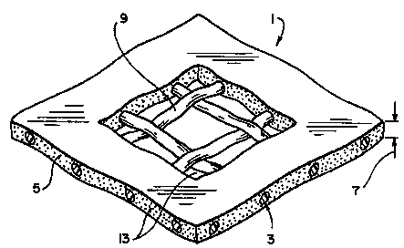
FIG.1 is a partial cross-sectianal perspective view of one C~
of the variable voltage protection component with a center portion removed to
show the reinforcing layer is a woven glass mat;
FIG. 2 is a cross-sectional view of another e L " of the present
invention wherein the reinforcing layer is non-woven glass mat;
FIG.3 is a cross-sectional view of another ~ L ' of the present
invention mounted on a conductive ground plane wherein the reinforcing layer
is non-woven glass mat with spacers;
FIG. 4 is a ~,.u~.. s - ~liu~l view of yet another ' ' of the
present invention wherein the reinforcing layer is sized spacers;
FIG. 5 is a cross-sectional view of the variable voltage protection
component of FIG. 4 with smaller sized spacers;
FIG. 6 is a perspective view of an integrated circuit chip carrier utilizing
the present invention;
FIG. 7 is a p.,.~_live view of a telephone connector utilizing the
present invention;
FIG. 8 is a partial cross-sectional perspective view of the present
invention installed on the edge of a printed circuit board;
FIG. 9 is a p~ .... ....view of a st~mdard packaged variable voltage
protection device in accordance with the present invention;
FIG.9A is a cross-sectional view of another . ' ~ ' of a standard
packaged variable voltage protection device in accordance with the present
invention;
3û FIG. 10 is a ~ live view of a lead frarne for producing variable
voltage protection devices;
~ wos6l0zs22 21 9 4 9 68 r~ r~- ~
. }7-
FIG. 11 is an integrated circuit chip lead frame with a variable voltage
protection component of the present invention installed;
FIG. 12 is a cross-secfional view of the chip lead frame of FIG. 11
along line 12-12;
FIG. 13 is a discrete variable voltage protection component in
a ' with the present invention;
FIG. 14 is a cross-sectional view of a printed circuit board with the
variable voltage protection component of the present invention laminated in the
printed circuit board;
FIG 15 is a cross-sectional view of another device utilizing the variable
voltage protection component of the present invention to contact a
~,.,1~ ' pattem of leads;
FIG. 16 is a cross-sectional view of an integrated circuit chip lead frame
with a variable voltage protection component of the present invention installed
across a die pad ground;
FIG 17 is a cross-sectional view of an alternate ~ I " of a
printed circuit board utilizing the variable voltage protection component of thepresent invention; and
FIG. 18 is a cross-sectional view of another L ' of an
integrated circuit chip lead frame with a variable voltage protection component
installed.
DEIATT Fn DF-~t'RTPllON OF ~IE INVF.l~TION
In one e ' " of the present invention (FIG. 1), there is provided a
variable voltage protection component 1 comprising a reinforcing layer 3
embedded in the voltage variable material 5, or in other words the reinforcing
layer is ~, ' with the voltage variable material. The reinforcing layer 3
has low , ~.aa;b;lily and is selected to be of ~re ~ ~ ' thickness so that
the variable voltage protection component I will have a ~ ,; ' uniform
thickness 7. By using the reinforcing layer 3 to achieve a uniform thickness,
repeatable electrical ~ r, can be achieved.
W096/02922 21 94q68 r~l~u. ~ ~
Preferably, the reinforcing layer 3 is a low co~ c~;l,ility fabric which
has a low coefficient of thermal expansion and a low dielectric constant. The
reinforcing layer 3 can be any of a m1mber of insulating materials including,
but not limited to, a porous polymer support material such as referred to in
U.S. Patent No. 4,950,546 (Dubrow et al.) and disclosed in U.S. Patent
Application Serial No. 711,119 filed March 12, 1985, (equivalent disclosure
published as European Patent Application EP 194872 on September 17, 1986),
porous synthetic resin polymer tape such as that sold under the trademark
"TEFLON" ( ' cd by E.I. du Pont de Nemours & Co., ~;h~ ;tun,
Delaware), ,ool~ lcac, glass, aromatic polyamide such as that sold under
the trademark "KEVLAR~ ( r ' 1 by E.I. du Pont de Nemours & Co.,
Wilmington, Delaware), polyester, i' r~ "~ polymer, i'
polymer, epoxy, and ceramic. The reinforcing layer 3 can be comprised of
fibrous pieces of insulating material 9 forming a mat as shown in FIG. 1 or
particulate pieces of insulating material 11 forming a non-woven mat as shown
in FIG. 2. The non-woven mat can be comprised of random particulate pieces
pressed or bonded together to form al sheet. The pieces can be pressed and
aligned so as to be all substantially horizontal. Further, the non-woven mat canbe the woven fibers of the mat shown in FIG. 1 broken, cut or chopped into
smaller pieces. In addition, the fibers or pieces of insulating material can be
coated with a metal coating provided that they are distributed so as to not create
a short or can be metal particles coated with insulating materials.
The reinforcing layer 3 includes a number of voids or spaces 13 between
the pieces 9 of insulating material in the mat (or pieces 11 in the non-woven
mat) comprising the reinforcing layer. In one; ' ' t, the voltage variable
material 5 , ~ the reinforcing layer 3 so that there is a continuous path
15 of voltage variable material from the top surface 17 to the bottom surface 19(FIG. 2). The reinforcing layer 3 c;m be illl~ ' with the voltage variable
material by a variety of methods as will be ~. ' by one of ordinary skill
in the art such as: dipping the reinf~)rcing layer in voltage variable material
then squeezing the reinforcing layer between two rollers; painting or pasting the
~ wo96/0292~ 2~ 94968 P~
voltage variable material across the reinforcing layer; casting; . S ,1~ , etc.
There should be a sufficient amount of voltage variable material S filling the
voids 13 to carry voltage spikes or current which occur in an ~ ,v, ' ~
condition. The voltage variable material can be continuous across the top and
S bottom surface of the variable voltage protection component so that the
can be universally used across variable lead pattems on a circuit
without precision tooling. Depending on the size of the conductive particles in
the voltage vaiiable materials, a small number of conductive particles or a large
number may be present in the voids 13. For example, if the conductive
10 particles are relatively large few particles will ft into the voids therefore more
will be on the top surface if the variable voltage material is applied on only the
top surface. In a like manner, more conductive particles will be on both the
top and bottom surface if the variable voltage material is applied to both the top
and bottom surfaces. Whereas if the particles are relatively small more
15 particles will pass into the voids.
In anotlier I ho~li . the reinforcing layer 3 is embedded in the
voltage variable material 5. The reinforcing layer can be imbedded in the
voltage variable material by a variety of methods as will be a~ ' by
those of ordinary skill in the art such as coating a substrate with the voltage
20 variable material then laminating the reinforcing layer into the wet coating;preparing a layer of voltage variable material then pressing the reinforcing layer
into the voltage variable material, etc.
The voltage variable ~ of the variable voltage protection
l are detemmined by the voltage variable material used and the
25 tbickness of the , The greater the thickness the higher the clamp
voltage. If a clamp voltage between about 20 to 30 volts is desired a typical
thickness 7 for the variable voltage protection component would be .8 to 1.0
mils. If a clamp voltage between about 30 to 40 volts is desired a typical
thickness would be 1.0 to 2.0 mils. If a clamp voltage between 40 to 70 volts
30 is desired a typical thickness would be 2.0 to 3.0 mils.
W0 96102922 2 1 9 4 q 6 8
-10-
FIG. 3 illustrates that insulating spacers 21 such as ceramic or glass
spheres can be added to the reinforcing layer 3 (mat or non-woven mat) to
morc accurately control the thickness 7. The spacers 21 extend between the top
surface 17 and bottom surface 19. If a ~ , c~ force is applied to the
S variable voltage protection component the spacers 21 will act as supports and
prevent the voltage variable material from being . . l, thus preventing
shorts or reductions in the clamp voltage. In particular, the resistance to
pressure is important during processing at the curing i . c. The spacers
21 can be any ~ " ~ size as clictated by the ~ (i.e., the
10 clamp voltage, etc.) desired for the variable voltage protection, , For
example, if a 1 mil thick variable voltage protection component is desired then
the spacers should be 0.9 to I . I mils, and preferably I mil. In general, the
spacers for most desirable voltage variable protection . , are between
0.2 to 10 mils in width. It is ~ , ' ' that the spacers can be other shapes
lS other than spherical. The size and sh,ape of the spacers is also dependent on the
size of the metal particles in the voltage variable material.
FIG. 3 further illustrates that the variable voltage protection component
1 can be attached to a conductive grolmd plane 23 to form a variable voltage
protection device 25. The variable voltage protection component can be
20 attached to the ground plane 23 by conductive adhesives, conductive primers,
non-conductive primers, direct bonding, etc. In addition, the variable voltage
protec'don component 1 can be attached to the ground plane 23 by processes
such as spraying, rolling, spin coating, l ~ molding or extruding. For
example, the conductive ground plane 23 can be a ~,.c ' ~ ' length and the
25 variable voltage protection component 1 can be laminated to the ground plane
23 or the variable voltage protection component I and the ground plane 23 can
be continuous reels and combined in an extrusion or lamination process.
The conductive ground plane '23 can be any of a variety of electrically
conductive materials known to one Or ordinary skill in the art such as copper,
30 nickel plated copper, brass, beryllium copper, etc. The conductive ground
~ w096102922 2l 94968
plane 23 can be flexible (such as a foil) so that it can conform to irregular
services.
In yet anoth.er ~ ,l.o~ " the conductive ground plane 23 is preferably
~- 1 With the cv~ .;l,le conductive ground plane 23, the va~.able
voltage protection device 25 cFin be p.aced or ~d between an electrical
lead and a metal lead, such as an outer cover of a connector without changing
the thickness of the variable voltage protection component 1 and thus preventingshorts and ensuring reliable e.ectrical ~ and clamp voltage. The
' '- ground plane 23 can be any of a variety of materials such as
10 conductive polymeric materia'., conductive silicon epoxy, cured conductive
silicone rubber, conductive primers, etc. Preferably, the ~ ..;I,Ie ground
plane is a conductive elastomer or conductive rubber. The ~ ' '
conductive ground plane can be eit.her electrically conductive at a'.l voltages or
electrica'.ly conductive only at high voltages similar to t.he voltage variable
materia'..
n another ' " t, t.he conductive ground plane 23 has a compliant
~ ~ on at least one surface so that the variable voltage protection device
can confor.n to irregular surfaces. In addition, t..e conductive ground plane can
have at least one adhesive surface so t.hat the conductive ground p.~.ne will
20 adhere to and maintain electrica. contact with an electrical component surface.
Preferably, the adhesive surface will have "quick stick" capability when it is
pressed into place.
F.GS. 4 and 5 illustrate t.hat the reinforcing layer 3 can be comprised of
spacers 21 only. In FIG. 4, t.he spacers 21 extend between the top surface 17
and bottom surface 19 as discussed above to form a reinforcing layer of desired
th.ickness 7. The voltage variable material 5 fills t.he voids 13 between the
spacers to provided a continuous path between the top and bottom surface. In
FIG. 5, the spacers 21 act in the same way but are smaller sized spheres which
are stacked on top of one another to form the reinforcing layer of desired
thickness 7. The spacers 21 can be of any desired shape and size and stacked
in as many layers as desired to form the reinforcing layer.
w096/02922 21 ~49 68 r~ a. ~. ~n.~ ~
The voltage variable material 5 used in accordance with the present
invention can be any voltage variable material known in the art, for example
those disclosed m either U.S. Patent No. 4,977,357 (Shrier) or U.S. Patent No.
4,726,991 (Hyatt et al.), which are illCUllJ~ ' ' herein by reference.
5 Generally, the voltage variable material comprises a binder and closely spacedconductive particles h.~....,c, .. u 1~ ,distributed in the bmder and spaced to
provide electrical t ~ In addition, various material such as that
disclosed in U.S. Patent No. 4,103"'74 (Burgess et al.) can be used im
accordance with the present inventio:n.
Preferably, however, the vollage variable material 5 can be a voltage
variable thick film paste typically comprised of 50% solvent and 50% solids
coating, the solid phase of which is comprised ûf 387c by weight (30% by
volume) of conductors such as 10 micron aluminum, 3.5% by weight (3.4 %
by volume) silica coating for the ~ ' , and 58.57c by weight (66.6% by
15 volume) of reinforced fluoro-silicone polymer whose dielectric breakdown
strength has been modifled through the addition of: ' and stabilizers
such as specifically sized aluminum oxide. The size of the aluminum oxide can
range from 0.01 to 5 microns. The voltage variable material cam also be a
solid which is laminated to the reinforcmg mat. The voltage variable material
20 can also be prepared as disclosed in cornmûnly assigned U.S. Patent
Application Serial No. 08/275,154 filed on 14 July 1994.
The variable voltage proteCti~Dn component I of the present mvention can
be used in a variety of ~ ;.. For example, the variable voltage
protection compûnent 1 cam be used with a conductive ground plane 23 to form
25 a variable voltage protection device 25 to be used in an integrated crrcuit chip
carrier 27 (E~IG. 6). The integrated circuit chip carrier 27 contains imtegratedcircuit chip 29. The conductive input/output pads (not shown) of chip 29 are
typically wire bonded by wires 31 to conductive leads 33 m the chip carrier 27.
The variable voltage protection com.ponent 1 contacts the conductive leads 33 of30 the chip carrier 27 and the conductive ground plane 23 is typically grounded to
wos6/02s22 21 9 4 9 68 r~
one or several system grounds in the chip carrier 27 or any other
point in the chip package.
The variable voltage protection device 25 cove}s a portion of each of the
conductive leads 33 of the chip carrier 27 leaving a portion of each conductive
lead 33 available for wire bonding of the chip 29 with wires 31. In another
. ..,1.~: --- .a, the conductive leads 33 can be wire bonded to the chip 29 and the
variable voltage protection device 25 is a lid that covers chip 29 and the
conductive leads 33.
In one ~ . .1.,,.1;".. -.~, the variable voltage protection device can be formedon the chip carrier 27 by first placing the variable voltage protection component
1 on the O,~J~IU, ' ' areas of the conductive leads 33 and then attaching the
conductive ground plane 23 to the variable voltage protection component 1.
Then connecting the conductive ground plane 23 to a system ground in the chip
carrier 27 or any other ~ , point in the chip package, as discussed
above. The variable voltage protection device 25 in the chip carrier 27 allows
all of the inputloutput leads to be in contact with the variable voltage protection
component I which is in turn in contact with the conductive ground plane 23.
Therefore, any ~ . vulLt,_ spikes which enter the package through any
lead or conductive pad can ' 'y pass through the variable
voltage protection component I to the conductive ground plane 23. The
variable voltage protection component 1 can be connected to conductive leads
33 by conductive adhesive or other ~ means. In addition, the variable
voltage protection component can be stamped and heat laminated directly to the
leads in a manner similar to tape automated bonding.
Another application of the variable voltage protection component I of
the present invention is any of a variety of electrical connectors such as RJ
(i.e., telephone), coaxial, D-Sub (i.e., multiple pin computer cable . ~,
38999 (i.e., aircrafQ, ARINC, SCSI (small computer systems interfacc), printed
circuit board input/output , chip socket (pin grid arrays, PLCC), etc.
The variable voltage protection component is essentially the same in all of the
electrical connectors except for the shape such as lc " ' for D-Sub or
wo s6/02s22 2 1 9 4 9 6 8 P 1~
-14-
circular for 38999 connectors. In each connector the design will be the same in
that there will be a variable voltage protection component in electrical
~ with a connector pin on one surface, and in contact with a
ground or a conductor that goes to system ground on another surface.
S Therefore, only the RJ connector will be described for illustrative purposes.
The variable voltage protection component I can be used with
conductive ground plane 23 to form a variable voltage protection device 25 to
be used in an RJ electrical connector 35 (FIG. 7). The RJ electrical connector
35 is comprised of insulating housing; 37 having a mating connector opening 39
10 for receiving a mating connector, suc:h as a telephone jack. The insulating
housing 37 also has a variable voltage protection device slot 41 for receiving
the variable voltage protection device: 25. In the variable voltage protection
device slot 41 is a plurality of electrical leads 43. The variable voltage
protection device 25 is placed in the variable voltage protection device slot 4115 with the variable voltage protection component 1 contacting the electrical leads
43. Forward end 47 of electrical colmector housing 45 is inserted in receiving
slot 49 and pushed forward until housing cover 51 is located over the variable
voltage protection device 25 and guide 53 is fully inserted in guide slot 55.
The housing cover 51 can be biased in toward conductive ground plane 23 so
20 that good electrical contact is made. Preferably, conductive ground plane 23 is
il,le to prevent pressure being trmsmitted to the u.-~vulLge protection
component 1, thus preventing shorts or variations in the clamp voltage. Any
u ._l v, " ~ spikes which enter the ellectrical connector 35 through any of the
leads 43 can " 'y pass through the variable voltage protection
25 component I to the conductive ground plane 23, then to the connector housing
45 through housing cover 51 to be shunted off to ground.
In another arrlir~tinn~ the variable voltage protection component I can
be used as webbing, tape, a label, or a film (FIG. ~) which can be custom cut
to desired lengths for applying to un,even and irregular surfaces, such as on
30 printed circuit boards. The variable voltage protection device comprised of the
variable voltage protection component I and conductive ground plane 23 can be
wos6/02s22 21 94968 P~u
adhered to a printed circuit board 57 with adhesive tape 59. The variable
voltage protection component 1 overlays any number of exposed printed circuit
leads 61. A ground 63, such as a wire, conductive epoxy, solder, etc. is
connected from a designated ground lead on the printed circuit board to the
5 conductive ground plane 23 through any of the openings 65 in the adhesive tape59. The opening 65 can also be one continuous slot. An u._1vulLb~ spike in
any of the printed circuit leads can ~ , pass through the variable
voltage protection component 1 to the conductive ground plane 23, then be
shunted off to ground. In another; ' ~ ' t, the variable voltage protection
lû cr~m.~nPnt adheres itself to the printed circuit board, so that adhesive tape 59
can be omitted.
The variable voltage protection component can be put into standard
packagmg , such as small outline, ~' i.. 1;~.~, packages, and dual-
in-line packages for
15 use in printed circuit boards. A small outline package 67 (FIG. 9) is
illustrative of each of the packaging styles. The small outline package 67 is
comprised of multiple pins 69 with the variable voltage protection component 1
connecting each of the pins. A common conductive ground plane 23 contacts
the variable voltage protection component 1. A ground pin 71 is connected to
2û conductive ground plane 23 by connection 73. Standard connecting techniques
such as wire bonding, soldering, or conductive epoxy can be used for
connection 73. To protect the device a protective covering such as epoxy or
standard molding compound c. n be used to mold around the device to seal the
vq~ql~ voltage protection . t-conductive ground plane interfaces to
25 protect the device.
The small outline package 67 is attached in parAllel to a printed circuit
on a printed circuit boards to provide u . _. v,1 ~ protection to the circuit. In
the absence of an u._1vulLb_ situation, the small outline package 67 sits
passively, not affecting the printed circuit. However, if am overvoltage is
30 present the variable voltage protection component 1 conducts the spike to the system ground through the conductive ground plane 23 and ground pin 71.
w0 96/02922 2 1 9 4 9 6 8 P~
-16-
Figure 9A shows a device 68 similar to the small outlme package 67,
but can be any standard packaging component as discussed above. The device
68 is comprised of multiple input leads 70 on one side of the device and
multiple groumd leads 72 opposite of the input leads 70. Variable voltage
5 protection component 1 commects the input leads 70 to the ground leads 72. A
common conductive ground plane 23 contacts the variable voltage protection
component 1. As with the device shown in FIG.9, the device 68 can be
covered with a protective covermg such as epoxy or standard molding
compound.
The device 68 is attached to a printed crrcuit m parallel the same as the
small outline package 67 discussed above. In the absence of an uv~lv~Jlti.v~,
situation, the device 68 sits passively. However, if an ~ ,. v, ' v is present in
any of the input leads 70 the variablle voltage protection component 1 conducts
the spike to the common ground plane 23 then to the system groumd from the
15 common ground plane 23 through any or all of the groumd leads 72.
As illustrated in FIG. 10, an,y of the packaged ~ can be
produced in a discrete, semi . ' or fully automated assembly process
using a discrete lead frame (typically about 7 inches in length with 40 lead sets
or die pads) or a continuous reel lead frame 75. The lead frame acts as a
20 conductive substrate. In one clllb~ ' t, the lead frame 75 has feed rails 77
with guide holes 79 for aligning and feeding the lead frame through the
,.. . -r . ~ V process. Other aligning and feeding means, as are known by
one of ordinary skill in the art, can be used such as stationary guide rails
abuttmg the side of the feed rails 7'7 and friction wheels pulling or pushing the
25 lead frames through the process.
In one l ' ' t, the variable voltage protection component 1 is
deposited on the lead frame 75. A thin insulating primer can be applied to the
lead frame to help the variable voltage protection component adhere to the lead
frame, or the variable voltage prote:ction component can be bonded to the lead
30 frame by r ~ ~, conductive adhesives, conductive epoxy, pressure,
hll.~ , spraying, rolling, spin coating, molding, extruding, etc. Then the
1~ W~9610197.2 21 94968 r~",... ~ - ~
~17-
conductive ground plane 23 is attached to the variable voltage protection
component 1. Each of the ground pins 71 is then attached to the conductive
ground plane 23 by connection 73. For making device 68, the ground leads are
not attached to the ground plane 23. After pac"aging, each of the lead sets 81
are diced out of the lead frame 75 for forming into the standard packages
illustrated in FIGS. 9 and 9A. The lead frame 75 shown in FIG. 10 has eight
leads per lead set 81, however, the lead frame can have any number of desired
leads.
It is: that the steps just described can be done in differing
order, such as the variable voltage protection component I can be applied to theconductive ground plane 23 and die stamped-out before being attached to the
lead sets (or die pads) 81. Or the conductive ground plane 23 can be connected
to the ground pin 71 after the lead sets have been diced from the lead frame 75.In another; ' ' t, the method of making the packaged devices can
be a fully automated process, such as a spraying, rolling, l ~ ~ or
extruding process, in which the lead frames are continuous with multiple lead
frame pins 69 ~.~ndi.,ul~u to the feed rails 77 and the variable voltage
protection component l is applied to the lead frames. For example, the
variable voltage protection component 1 and conductive ground plane 23 can be
in continuous tapes that are laminated to the continuous lead frames. Then the
assembled . . can be divided into a p.c ' ' number of leads.
For the device illustrated in FIG. 9, one lead can be selected as the ground pinand connected to the conductive ground plane.
In other ' - " the lead frame 75 can be a conductive substrate
having a l ~ ' pattern matching the leads on a printed circuit board or
the conductive substrate can be a continuous sheet that is photo-etched to form
a ~lcJ~; ' pattern to match the leads on a printed circuit board or an
integrated circuit. Then the 1 ' . c .~ h~ areas are filled with voltage variable
material.
FIG. 11 shows another application of the present invention, wherein the
variable voltage protection device 25 can be used in tape form on an integrated
w0 96/02922 2 1 9 4 t!, 6 8
circuit chip lead frame 83. The integrated circuit chip lead frame has a
plurality of leads 85 connected to an integrated circuit chip 29 and for
connecting to a printed circuit boarcl or multiple chip module. As can be seen
in FIG. 12, the variable voltage protection device 25, comprising variable
5 voltage protection component 1 and conductive ground plane 23, is "taped"
across the plurality of leads 85. The leads 85 are connected to the chip 29 by
wires 31. Each strip of conductive ground plane 23 can be attached to a system
ground when the integrated circuit chip lead frame 83 is attached to a printed
circuit board or multiple chip module.
In another ~ ~b~l; .1 utilizing the integrated circuit chip lead frame
83, the variable voltage protection c omponent can be applied across the leads
85 and die pad ground 109 on the bottom of the integrated circuit chip le~d
frame 83 (FIG. 16). The die pad ~round 109 is connected to system ground
when the integrated circuit chip lead frame 83 is attached to a printed circuit
15 board or multiple chip module. In this way, when one of leads 85 P ~
a voltage spike, the variable voltage protection connponent I conducts the spikelaterally through the variable voltage protection component to the die pad
ground 109 to protect chip 29. Optionally, ground plane 23 can be added for
better ~ - by the variable voltage protection device. With the ground
20 plane 23 attached, when one of leads 85 ~ - a voltage spike, the
variable voltage protection component I conducts the spike to ground plane 23
then to the die pad ground 109.
In yet another ~ o-l;. ..l utilizing an integrated circuit chip lead frarne
wire bonded by wires 31 to chip 29, the variable voltage protection component
can be applied between the leads 85 and die pad ground 109 ~FIG.18). The die
pad ground 109 is connected to system ground when the integrated circuit chip
lead frame is attached to a printed circuit board or multiple chips module.
When any of the leads 85 f ~ a voltage spike, the variable voltage
protection component 1 conducts the spike to the system ground through die
pad ground 109.
I~ WO96/0~9~ 21 94~8 r~J~
~ -19-
A discrete surface mount device 87 is shown in FIG. 13. The device 87comprises a composite of variable voltage protection component 1 l~;.,h~
between two conductive ground planes 23, and two outer conductive layers 89
for surface mounting the device 87. The layers of the composite can be
5 assembled using a laminating or coating process. A protective coating of epoxycan be applied (such as by painting) to the device 87 to protect the variable
voltage protection component 1.
In FIG. 14, the variable voltage protection device 25 is laminated into a
printed circuit board 91 having signal leads 93. The variable voltage protectioncomponent 1 is applied to or around the signal leads 93. Layers 95 on either
side of the variable voltage protection device 25 and signal leads 93 make up
the printed circuit board. The conductive ground plane 23 is attached to a
system ground. If a signal lead ~ ~ an u._.v~ ' ~ situation, the
variable voltage protection component 1 conducts the spike to the conductive
15 ground plane 23 which shunts it off to the system ground.
In another ~ hu ~ the variable voltage protection component I can
be utilized in a printed circuit board 91 using the vias or IhlU~ h ~ IP~ 111 inthe printed circuit board (FIG. 17). The vias 111 can be lined with variable
voltage protection component 1 that contacts a ground plane 23, and the signal
20 leads 93 in the printed circuit board. It is important that the ground plane 23
terminates at the variable voltage protection component 1. It is also important
that the signal leads 93 extend through the variable voltage protection
component 1 to contact a layer of conductive material 113, such as solder,
which overlays the variable voltage protection component 1. In this way, when
25 a pin (not shown) is inserted in via 111 the pin is in electrical
with signal lead 93. If signal lead 93 l~ an u._lv~ situation, the
variable voltage protection component 1 conducts the spike to ground plane 23
which shunts the spike off to system ground
~ FIG. 15 shows a device 97 utilizing the variable voltage protection
30 component 1 to contact a ~l~l.,; ' pattern of signal leads 99 and ground
leads 101. A conductive strip 103 has a pattern of conductive bumps 105,
w096/02922 21 94~ 68 r~"u~
-20-
which are etched, stamped or machinedl to match a 1~ .l pattem of
ground leads 101. The variable voltage protection component 1 is placed
between the conductive bumps lOS is fllattened off to be even with the
conductive bumps 105. A layer 107 of conductive nnaterial, such as conductive
5 epoxy or conductive adhesive, is applied to the conductive bumps 105 and
variable voltage protection component I to match tlne 1~ " ' pattem of
signal leads 99 and ground leads 101. When one of the signal leads 99
C an ~ .v~JlL e spike, the variable voltage protection component
conducts the spike to the conductive strip 103. Then the spike is conducted
through the layer 107 of conductive material to the ground leads 101. In
addition, layer 107 of the device 97 can be omitted and the variable voltage
protection component I can be adhered directly to the leads.
The foregoing has described the principles, preferred ' ' and
modes of operation of the present invention. However, the invention should
lS not be construed as being limited to the particular; ' ' discussed.
Tlnus, the above-described ~ ~ ' should be regarded as illustrative rather
than restrictive, and it should be ~ ' that variations may be made in
those ,--~ - ~"~ by workers skilled in the art without departing from the
scope of tlne present invention as defined by the following claims.