Note : Les descriptions sont présentées dans la langue officielle dans laquelle elles ont été soumises.
CA 02196007 1999-07-12
VARIABLE-FREQUENCY RESONATOR, VARIABLE-FREQUENCY OSCILLATOR,
AND VARIABLE-FREQUENCY FILTER
The present invention relates to variable-frequency
resonators, variable-frequency oscillators, and variable-
frequency filters used in microwave- and millimeter-wave-
frequency communications.
Dielectric resonators have many features such as high Q
values, low dependance of the resonant frequency on temperature,
and the advantage of being made compact at low cost. Hollow
resonators and stripline resonators, which have been used in
various fields for a long period, have recently been gradually
replaced with dielectric resonators.
Embodiments of the present invention and certain prior
art arrangements are illustrated in the accompanying drawings, in
which:
Fig. 1 is a plan of a variable-frequency resonator
according to a first aspect of the present invention.
Fig. 2 is an equivalent circuit diagram of the resonator
shown in Fig. 1.
Fig. 3 is a characteristic chart of the resonator shown
in Fig. 1.
Fig. 4 is a plan of a variable-frequency resonator
according to a second aspect of the present invention.
Fig. 5 is an equivalent circuit diagram of the resonator
shown in Fig. 4.
-1-
CA 02196007 1999-07-12
Fig. 6 is a cross section of a variable-frequency
resonator according to a third aspect of the present invention.
Fig. 7 is a partial perspective view of a variable-
frequency filter according to a fourth aspect of the present
invention.
Fig. 8 is a cross section of a main part of the
variable-frequency filter.
Fig. 9 is a plan of the main part of the variable-
frequency filter.
Fig. 10 shows a configuration of a diode board used in
the variable-frequency filter.
Fig. 11 is an equivalent circuit diagram of the
variable-frequency filter.
Fig. 12 is a plan of a main part of a variable-frequency
filter according to a fifth aspect of the present invention.
Fig. 13 is a plan of a main part of a variable=frequency
filter according to a sixth aspect of the present invention.
Fig. 14 is a characteristic chart of the variable-
frequency filter.
Fig. 15 is a plan of a main part of a variable-frequency
oscillator according to a seventh aspect of the present
invention.
Fig. 16 is a cross section of the main part of the
variable-frequency oscillator.
Fig. 17 is a plan showing a configuration of a circuit
board of a variable-frequency oscillator according to an eighth
aspect of the present invention.
-2-
CA 02196007 1999-07-12
Fig. 18 is a cross section of the variable-frequency
oscillator.
Fig. 19 is a plan showing a configuration of a portion
to which a pin diode is mounted.
Fig. 20 is a partial perspective view showing coupling
between electrodes to which the pin diode is connected and non-
radiative dielectric lines.
Fig. 21 is a plan showing a portion to which a pin diode
is mounted in a variable-frequency resonator according to a ninth
aspect of the present invention.
Fig. 22 is a plan showing a configuration of a circuit
board in a variable-frequency oscillator according to a tenth
aspect of the present invention.
Fig. 23 is a cross section of the variable-frequency
oscillator.
Fig. 24 is a plan showing a configuration of a portion
to which a gun diode is mounted in the variable-frequency
oscillator.
Fig. 25 is a plan showing a configuration of a circuit
board in a variable-frequency oscillator according to an eleventh
aspect of the present invention.
Fig. 26 is a plan of a main part of a variable-frequency
oscillator according to a twelfth aspect of the present
invention.
Fig. 27A shows a configuration of a conventional fixed-
frequency oscillator.
Fig. 27B shows a configuration of a conventional
variable-frequency oscillator.
-3-
CA 02196007 1999-07-12
In an oscillator employing a conventional dielectric
resonator 3, shown in Fig. 27A, a microstripline 1 is disposed in
the vicinity of the dielectric resonator 3. A terminating
resistor 4 and a field effect transistor (FET) 5 are connected to
the ends of the microstripline 1. A part of a signal input
through the FET 5 is reflected near the coupling point between
the dielectric resonator 3 and the microstripline 1 and amplified
by the negative resistance of the FET 5. As a result, the FET 5
outputs an oscillating signal. This is due to the generation of
injection locking. In other words, in the signal input through
the FET 5, only a component having the same frequency as the
resonant frequency of the dielectric resonator 3 is reflected
near the coupling point and returned to the FET 5.
Therefore, the stability of the oscillation frequency
with respect to temperature of the oscillator depends on the
resonant frequency of the dielectric resonator 3. As described
above, since the resonant frequency of the dielectric resonator
3 slightly depends on temperature, the oscillator has a highly
stable oscillation frequency with respect to temperature. Since
the dielectric resonator has a high Q value, a good C/N ratio is
obtained.
To use an oscillator with the dielectric resonator and
the microstripline as a frequency-modulation (FM) oscillator, the
oscillation frequency needs to be variable. To this end, a
microstripline 2 serving as a sub line is provided close to the
dielectric resonator 3 in addition to the microstripline 1
-4-
CA 02196007 1999-07-12
serving as the main line, as shown in Fig. 27B. Moreover, a
variable-reactance device 6 such as a varactor diode is connected
to an end of the microstripline 2. Due to changes in voltage
applied to the variable-reactance device, the resonant frequency
of the dielectric resonator 3 changes, and as a result, the
frequency of the oscillating signal changes.
To make the resonant frequency of the dielectric
resonator variable by using the microstripline and the reactance
device, as described above, the dielectric resonator 3 needs to
be disposed near the microstripline 2 so as to be coupled with
the microstripline 2. Since a part of the resonant current
flowing through the dielectric resonator 3 also flows into the
metallic microstripline 2, and the reactance device 6 such as a
varactor diode has a low Q value, the Q value of the dielectric
resonator is reduced. Therefore, the C/N ratio becomes lower
than that of the fixed-frequency oscillator shown in Fig. 27A.
Since the reactance device 6 used for microwave and
millimeter-wave frequencies generally has a small capacitance,
with a stray capacitance added when the resonator is mounted on
a circuit board, the effective capacitance change rate lowers and
the variable-frequency range is narrowed. It is expected that
this problem also occurs in a variable-frequency resonator and a
variable-frequency filter having the configuration shown in Fig.
27B. Therefore, the variable-frequency resonator has a reduced
Q value. The variable-frequency filter has an increased
insertion loss.
-S-
CA 02196007 1999-07-12
Accordingly, it is an object of the present invention to
provide a variable-frequency resonator having a high Q value, a
variable-frequency oscillator having a high C/N ratio, and a
variable-frequency filter having a low insertion loss.
The foregoing object is achieved according to the
present invention through the provision of a variable-frequency
resonator including a main line; a sub line which is not directly
coupled with the main line; and a dielectric resonator coupled
with the main line and the sub line. In order to suppress a
reduction in Q value of the dielectric resonator due to the sub
line, the resonator also includes a.switching device disposed at
an intermediate position in the sub line. The electrical length
of the sub line changes according to an electrically
conductive/open state of the switching device, and the resonant
frequency of the dielectric resonator changes. The switching
device is not used for changing its reactance like a conventional
varactor diode but for just switching between the electrically
conductive state and the open state. As such a switching device,
a device having a high Q value such as a pin diode, for example,
can be used. A reduction in Q value of the dielectric resonator
can be suppressed.
In the variable-frequency.resonator, the main line and
the sub line may be microstriplines. The switching device may be
connected between an intermediate point of the sub line and the
ground, or between the sub line divided into two portions.
-6-
CA 02196007 1999-07-12
The main line and the sub line may be non-radiative
dielectric lines.
The main line and the sub line may be made up of non-
radiative dielectric lines in which a dielectric strip and a
circuit board are disposed between parallel electrically
conductive plates.
When non-radiative dielectric lines are used, since the
electrical length of the sub line coupled with the dielectric
resonator is switched according to an electrically
conductive/open state of the switching device, the resonant
frequency of the dielectric resonator is switched and a variable-
frequency resonator is implemented. Unlike a case in which
microstriplines are used, since a part of the resonant current of
the dielectric resonator does not flow into the sub line, even if
the dielectric resonator is strongly coupled with the non-
radiative dielectric lines, the dielectric resonator has almost
no reduction in Q value, and a variable-frequency resonator
having a extremely high Q value is implemented.
According to the present invention, a variable-frequency
oscillator and a variable-frequency filter having the same
configuration as described above can be made. This means that a
variable-frequency oscillator having a high C/N ratio and a
variable-frequency filter having a low loss can be implemented.
CA 02196007 1999-07-12
A configuration of a variable-frequency resonator
according to an embodiment of the present invention will be
described below by referring to Figs. 1 to 5.
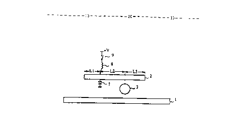
In Fig. 1, there is disposed a microstripline 1 serving
as a main line and a microstripline 2 serving as a sub line which
is not directly coupled with the microstripline 1. A dielectric
resonator 3 in the TEols mode is disposed such that it is
magnetically coupled with the microstriplines 1 and 2. Between
an intermediate point of the microstripline 2 and the ground, a
switching device 7 is connected. There is also provided a low-
pass filter 8 and a switch 9 for connecting and disconnecting a
bias voltage to the switching device 7. The switch 9 turns the
switching device 7 on and off.
Fig. 2 is an equivalent circuit diagram of the resonator
shown in Fig. 1. In Fig. 2, 01, 02, and 03 indicate the
electrical lengths of portions L1, L2, and L3 of the
microstripline 2 shown in Fig. 1, respectively, and SW and DR
correspond to the switching device 7 and the dielectric resonator
3. T1 and T2 are ideal transformers which form the magnetic
coupling between the dielectric resonator 3 and the main and sub
lines. Since the electrical length of the sub line which is
coupled with the dielectric resonator DR changes according to the
on/off state of the switching device, the
_g_
2~~~~~7
resonant frequency of the dielectric resonator DR changes.
Fig. 6 is a cross section of a variable-frequency
resonator. On the upper surface of a circuit board 10, a
microstripline 1 serving as a main line and a microstripline 2
serving as a sub line are formed. On the lower surface of the
circuit board I0, a ground conductor 11 is provided. Also on
the upper surface of the circuit board 10, a cylindrical
support base 12 having a low dielectric constant is mounted
and then a cylindrical TEoia mode dielectric resonator 3 is
mounted on it. The dielectric resonator 3 may have another
shape as required. The microstriplines 1 and 2 are
magnetically coupled with the dielectric resonator 3.
On the upper surface of the circuit board 10, a pin
diode for connecting a specified point of the microstripline 2
to the ground conductor and a circuit for supplying a bias
voltage to the diode are provided. The microstriplines 1 and
2, and the dielectric resonator 3 are disposed on the circuit
board 10 as shown in Fig. 1. The circuit board 10 is
surrounded by a shielding conductor 13 to form the variable-
frequency resonator.
Fig. 3 indicates an insertion loss between the input and
output sections of the main line shown in Fig. 2. The
resonant frequency obtained when the switching device SW is
open is named fort and the resonant frequency obtained when the
switching device SW is closed is named foa. when the switching
device SW is open, a signal having the frequency foft is
attenuated. then the switching device is closed, a signal
having the frequency foo is attenuated.
In the variable-frequency resonator, the distance
between the dielectric resonator and the sub line, and the
lengths of the portions of the sub line, L1, L2, and L3, are
determined such that a required variable-frequency range is
obtained. In the equivalent circuit shown in Fig. 2, the
resonant frequency changes by 410 MHz by turning on/off the
switching device SW when A1 = 02 = 40 degrees, 03 = 90 degrees,
Za = 50 ~, the coupling coefficient of T1 is 1:40, the
coupling coefficient of T2 is 1:50, the inductance L of the
dielectric resonator isØ7 nH, the capacitance C of the
dielectric resonator is 0.01 pF, the Q value of the dielectric
resonator is 5000, and the resonant frequency is 60 GHz.
Fig. 4 is an equivalent circuit diagram of a variable-
frequency resonator in which a switching device is inserted at
an intermediate point of a sub line. When a switch 9 is
closed, a bias voltage is applied to a switching device 7 to
close it. When the switch 9 is opened, the switching device 7
opens.
Fig. 5 is an equivalent circuit diagram of the resonator
shown in Fig. 4. Since the electrical length of the sub line
which is coupled with the dielectric resonator DR changes
according to the on/off state of the switching device, the
resonant frequency of the dielectric resonator DR can be
changed.
In the variable-frequency resonator shown in Fig. 6,
when signal input and output sections are provided for the
1~
219607
microstripline 1 serving as the main line, a component having
the same frequency as the resonant frequency of the dielectric
resonator 3 is trapped in the input signal. Therefore, a band
elimination filter is implemented which can switch the trap
frequency by switching the switching device.
A configuration of a variable-frequency filter according
to a second embodiment of the present invention will be
described below by referring to Figs. 7 to 11.
Fig. 7 is a partial perspective view of the filter With
an upper electrically conductive plate removed. There is
provided a dielectric strip 14 serving as a main line and a
dielectric strip 15 serving as a sub line in non-radiative
dielectric lines. A diode board 16 described later is put in
the dielectric strip 15 at an intermediate point. Between the
two dielectric strips 14 and 15, a dielectric resonator 3
sandwiched by support bases 12 is provided.
Fig. 8 is a cross section of the filter taken on a plane
70 passing through the filter. Fig. 8 indicates a state in
which the upper and lower electrically conductive plates 17
and 18 are mounted. The support bases 12 are made up of a
low-dielectric-constant resin or ceramic. The support bases
12 are not necessarily mounted in the upper and lower
directions of the dielectric resonator. Only one of them is
needed if the dielectric resonator 3 is secured apart from the
upper and lower dielectric plates.
Fig. 9 is a plan of the filter. The distance between
the dielectric resonator 3 and the dielectric stripline 15
219~~Q1
serving as the sub line, and the lengths of the portions of
the dielectric strip 15, Ll, L2, and L3, are determined such
that a required variable-frequency range is obtained.
Fig. 10 is a view showing a configuration of the diode
board 16. Two electrodes 19 are provided at portions against
which the dielectric strip 15 is butt when the filter is
i
i
assembled. Between the electrodes, a pin diode 7 is mounted.
When the pin diode is open, an LSM-mode signal which transfers
in the non-radiative dielectric lines passes through the
electrodes 19. When the pin diode is electrically conductive,
the signal is reflected by the electrodes 19.~ The electrodes
19 are connected to conductive patterns 20 including portions
having a low characteristic impedance and portions having a
high characteristic impedance alternately at an interval of
~,/4. The conductive patterns 20 serve as low-pass filters.
Since a bias circuit foi the pin diode is provided with the
low-pass filters, coupling between the bias circuit and the
dielectric strip 15 is avoided.
Fig. 11 is an equivalent circuit diagram of the
variable-frequency filter. since the dielectric resonator
operates in the TEoia mode, the dielectric resonator is coupled
with the dielectric strips 14 and 15. In the equivalent
circuit, they are coupled by capacitors as shown in Fig. 11.
since the electrical length of the non-radiative
dielectric line made up of the dielectric strip 15 and the
upper and lower electrically conductive plates changes
according to the on/off state of the pin diode, the resonant
239b~07
frequency of the dielectric resonator changes. Therefore,
when signal input and output sections are provided for the
non-radiative dielectric line, a variable-frequency band
elimination filter is implemented in the same way as shown in
Fig. 3. In other words, the frequency of the signal component
to be trapped by the dielectric resonator can be switched
among the externally input signal components. A multi-stage,
variable-frequency band elimination filter can be implemented
by differentiating the electrical lengths to be switched of
the dielectric strip serving as the sub line and by disposing
a plurality of the pairs along the dielectric strip serving as
the main line.
Fig. 12 shows a configuration of a variable-frequency
filter according to a third embodiment of. the present
invention. In the second embodiment, the diode board is
inserted at a point into the dielectric strip 15 serving as
the sub line. When the pin diode is turned on, the electrodes
19 shown in Fig. 10 become conductive, and the position of the
diode board becomes a short-circuit end of the dielectric
strip 15. If line isolation is insufficient, a plurality of
diode boards 16a and 16b are provided at an interval of ~g/4
as shown in Fig. 12 and both diodes are switched on/off at the
same time. With this configuration, the position away from
the dielectric resonator 3 by L2 serves as an equivalent
short-circuit position and the equivalent electrical length of
the dielectric strip 15 serving as the sub line is positively
switched.
t
2~96~D7
Fig. 13 and Fig. 14 show a configurationand
characteristic of a variable-frequency filter according to a
fourth embodiment of the present invention. Fig. 13
illustrates a state in which the upper electrically conductive
plate of the filter is removed. In this embodiment, two non-
radiative dielectric lines, dielectric strips 14a and 14b
(main lines), are disposed such that their ends are close to a
dielectric resonator 3. To prevent direct coupling between
these two dielectric strips 14a and 14b, and a dielectric
strip 15, the end faces of the dielectric strips 14a and 14b
are disposed as far as possible away from the end faces of the
dielectric strip 15 and the strips are disposed at specified
angles. The.resonant frequency of the dielectric resonator 3
is switched by switching on/off a pin diode provided for a
diode board 16. The insertion-loss characteristic of a signal
passing through the two dielectric strips 14a and 14b coupled
through the dielectric resonator 3 changes as shown in Fig. 14.
Fig. 15 and Fig. 16 show a configuration of a variable-
frequency oscillator according to a fifth embodiment of the
present invention. Fig. 15 illustrates a state in which the
upper electrically conductive plate of the oscillator is
removed. A diode board 16 is inserted at a specified position
into a dielectric strip 15 which constitutes a non-radiative
dielectric line serving as a sub line. At one end of a
dielectric strip 14 which is a non-radiative dielectric line
serving as a main line, a terminator 21 is provided. The
terminator is formed by mixing a resistor member with a resin
2196af~7
member which constitutes the dielectric strip 14. Between the
dielectric strips 14 and 15, a dielectric resonator 3 is
disposed. There is also shown a gun diode 22 and an
excitation probe 23. The excitation probe 23 is disposed
close to the dielectric strip 14 and perpendicular to the
direction in which electromagnetic waves transfer in the
dielectric strip 14.
Eig. 16 is a cross section of the variable-frequency
oscillator. On the upper and lower surfaces of the dielectric
strips 14 and 15, parallel electrically conductive plates 17
and 18 are disposed, and the dielectric resonator 3 is
disposed between the two electrically conductive plates 17 and
18. The gun diode 22 is embedded in a fixed block 160. The
excitation probe 23 is made up of an insulating board and an
electrically conductive pattern provided thereon. The gun
diode 22 is connected to the electrically conductive pattern
with wire or ribbon.
The dielectric resonator 3, the dielectric strip 14, and
the gun diode 22 form a band-reflective oscillator, and an
LSM-mode electromagnetic wave is transferred to the dielectric
strip 14. The oscillator selectively outputs a signal
component having the same frequency as the resonant frequency
of the dielectric resonator 3 among oscillating signal
components generated by the gun diode 22. Therefore, since
the dielectric resonator 3 has high frequency stability, the
oscillation frequency of the oscillator is stable.
The gun diode itself usually has a frequency stability
2~9~0~7
of about -100 ppm/°C with respect to temperature. Since the
dielectric resonator 3 has a frequency stability of 5 ppm/°C
or less with respect to temperature, the frequency stability
of the oscillator with respect to temperature is maintained at
ppm/°C or less. -
In this embodiment, the dielectric strip 15 is coupled
with the dielectric resonator 3,~and the resonant frequency of
the dielectric resonator 3 is switched by switching on/off the
pin diode on the diode board 16. With this switching, the
oscillation frequency of the gun diode 22 is switched.
Therefore, when a bias voltage applied to the pin diode on the
diode board 16 is turned on/off according to a modulation
signal, the oscillator serves as a frequency-shift-keying
(FSK) oscillator.
Since the dielectric stxips 14 and 15, and the diode
board 16 have almost no loss, even if the dielectric resonator
3 is strongly coupled with the dielectric strips 14 and 15,
the Q value has little reduction and a variable-frequency
oscillator having a high C/N ratio is obtained.
Figs. 17 to 20 show a configuration of a variable-
frequency oscillator according to a sixth embodiment of the
present invention. In the sixth embodiment, a main line and a
sub line are formed in non-radiative dielectric lines in which
dielectric strips and a circuit board are disposed between
parallel electrically conductive plates.
Fig. 17 is a plan of the circuit board. Fig. 18 is a
cross section taken from line A-A in Fig. 17 with the
Z1960~7
electrically conductive plates being disposed above and below
the circuit board shown in Fig. 17.
An upper dielectric strip 14a is disposed on the upper
surface of the circuit board 24, and a lower dielectric strip
14b is disposed on the lower surface of the circuit board 24.
The ends of the dielectric strips 14a and 14b are terminated
ti '
by resistor-member-film patterns 25.
At an intermediate point of a dielectric strip 15a
serving as a sub line, a pin diode and electrodes are disposed
as will be described later. The pin diode is connected to
conductive patterns 26 for supplying a bias voltage. Another
dielectric strip 15b is provided on the lower surface of the
circuit board 24, which is located under the dielectric
stripline 15a.
On the circuit board 24, a conductive pattern 27 for
applying a bias voltage to a gun diode is provided. An
electrode of the gun diode 22 is connected to the conductive
pattern 27 with wire or ribbon. The circuit board 24 is also
provided With an excitation conductive pattern 28. The
excitation conductive pattern 28 is connected to the other
electrode of the gun diode 22 with wire or ribbon. A
cylindrical dielectric resonator 3 is secured on the circuit
board 24 with adhesive. The dielectric resonator may have
another shape as required.
Since the excitation conductive pattern 28 is disposed
perpendicularly to the direction in which an electromagnetic
wave proceeds in the dielectric strips 14a and 14b, the
2196~d7
s
excitation conductive pattern 28 is coupled with an LSM-mode
magnetic field within the non-radiative dielectric lines, and
the oscillating signal generated by the gun diode transfers in
the non-radiative dielectric lines 14a and 14b. The
excitation conductive pattern 28 may be disposed such that a
tip thereof is in the vicinity of the dielectric strip 14a
without going inside the dielectric-strip 14a.
Fig. 19 is a partially enlarged view of the dielectric
strips shown in Fig. 17. Two trapezoidal electrodes 19 are
provided at a portion sandwiched by the dielectric strips 15a
and 15b, and a pin diode 7 is mounted between the electrodes
19. When the pin diode 7 is open, the two electrodes l9 serve
as slot lines. When the pin diode 7 is electrically
conductive, the electrodes 19 are short-circuited and a signal
transferring in the dielectric strips 15a and 15b is reflected
at the position where the diode is disposed.
Fig. 20 shows coupling between an LSM-mode
electromagnetic field and the electrodes 19 in the dielectric
strips 15a and 15b. An electromagnetic field distribution in
the slot lines is similar to that in the LSM mode in a non-
radiative dielectric line. When the electrodes 19 are
disposed in the direction in Which a signal transfers in the
dielectric strips 15a and 15b, the LSM-mode electromagnetic
field is coupled with the electrodes 19.
Fig. 21 shows conductive patterns for applying a bias
voltage to a pin diode according to a seventh embodiment of
the present invention. Electrodes 19 totaling ~/2 in length
2196007
are disposed perpendicularly to dielectric strips 15a and 15b.
The pin diode 7 is connected to the electrodes 19. Since a
conductor R/2 long is strongly coupled with an LSM-mode
magnetic field, a signal transferring the dielectric strips
15a and 15b is reflected at the position of the electrodes 19
when the pin diode 7 is electrically conductive. The signal
passes through the position of the electrodes 19 when the pin
diode 7 is open. Provided are ~/4 open stubs 26' to
equivalently short-circuit the roots of the electrodes 19.
Since both ends of the electrodes totaling ~/2 in length are
short-circuited, the middle becomes open. Therefore, a signal
coupled with the non-radiative dielectric lines when the pin
diode 7 is open does not go into the bias circuit for the pin
diode. A signal does not come from the bias circuit, either.
As a conductor for applying a bias voltage to the pin
diode 7, a suspended line or a coplanar guide may be used
instead of the microstriplines shown in Fig. 21. when a
grounding conductor on the circuit board needs to be connected
to the upper and lower electrically conductive plates, the
grounding conductor on the circuit board may be connected such
that it butts against a pillar-shaped protrusion which is
provided for the upper and lower electrically conductive
plates at a position so as not to interfere with operations of
components mounted on the circuit board or disposed between
the upper and lower electrically conductive plates.
A configuration of a variable-frequency oscillator
according to an eighth embodiment of the present invention
219601
will be described below by referring to Figs. 22 to 24. Fig.
22 is a plan of a main section of a circuit board. Fig. 23 is
a cross section taken from line A-A in Fig. 22 with upper and
lower electrically conductive plates being disposed above and
below the circuit board. On the upper surface of the circuit
board 24, conductive patterns 26 and 27 for applying bias
voltages to a pin diode and a gun diode, respectively, a
resistor film 25, and a ground conductor 29 are provided. An
upper dielectric strip 14a serving as a main line, an upper
dielectric strip i5a serving as a sub line, and a dielectric
resonator 3 are also disposed on the upper surface of the
circuit board 24. The gun diode is mounted such that it is
sandwiched by the upper dielectric strip 14a and a lower
dielectric strip 14b. In the same way, the pin diode is
mounted such that it is sandwiched by the upper dielectric
strip 15a and a lower dielectric strip 15b.
Fig. 24 is a partially enlarged view of Fig. 22. The
ground conductor 29 extends toward the dielectric stripline
14a forming a protrusion. A so-called bare-chip gun diode 22
is mounted at the protrusion. One electrode of the gun diode
22 is connected to an electrode 19 with ribbon or wire. By
using the bare-chip gun diode, the circuit board is made
compact.
Fig. 25 shows a configuration of a circuit board of a
variable-frequency oscillator according to a ninth embodiment
of the present invention.
A gate coupling pattern 31, an output terminal 33, and a
~~~b~~7
ground conductor 29 are provided on the circuit board at an
end of a dielectric strip 14a. An FET 30 is connected to
these conductors. There is also provided a conductive pattern
32 for supplying a gate bias voltage and a conductive pattern
34 for supplying a drain bias voltage. The rear surface of
the circuit board around the FET ~s provided with a ground
conductor so that the conductive patterns 32 and 34, and the
output terminal 33 form a microstripline. The other
configuration is the same as that shown in Fig. 17 or Fig. 22.
An oscillating signal can be obtained from the microstripline
by using the FET as a negative-resistance device. The FET may
be gate-grounded or drain-grounded.
A bare-chip FET may be used. A bare-chip FET may be
disposed between the dielectric strip 14a and the circuit
board. In this case, a non-radiative dielectric line may be
used as an output terminal.
Fig. 26 shows a plan of a main section of a variable-
frequency oscillator according to a tenth embodiment of the
present invention. On a circuit board, a conductive pattern
26 for applying a bias voltage to a pin diode, an excitation
conductive pattern 28, and a resistor film 25 are provided.
The conductive pattern 26 for supplying the bias voltage
extends to the inside of a strip 15a, and its tip is connected
to the pin diode. Another strip 15b is disposed on the rear
surface of the circuit board below the strip 15a to form a
non-radiative dielectric line.
An upper dielectric strip 14a serving as a main line is
Z
2196d~1
also disposed. On the rear surface of the circuit board, a
lower dielectric strip 14b is disposed at the position
opposite that of the strip 14a to form a non-radiative
dielectric line. The dielectric strips 15a and 15b serving as
the sub lines are disposed perpendicularly to the dielectric
strips 14a and 14b serving as the main lines. A dielectric
resonator 3 is disposed therebetween. An end of the
dielectric strips 14a and 14b is terminated by the resistor
film 25. A gun diode 22 is disposed below the circuit board.
Through an opening of the circuit board, an electrode of the
gun diode 22 is connected to an excitation conductive pattern
28 with ribbon or wire. With this configuration, namely, with
a configuration in which the dielectric strips 15a and 15b
serving the sub lines are disposed perpendicularly to the
dielectric strips 14a and 14b serving as the main lines, with
the dielectric resonator 3 disposed therebetween, the
dielectric strips 14a and 14b are electrically coupled with
the dielectric resonator 3, and the dielectric strips 15a and
15b are magnetically coupled with the dielectric resonator 3.
ZZ