Note : Les descriptions sont présentées dans la langue officielle dans laquelle elles ont été soumises.
CA 02196468 1999-12-07
FREQUENCY ESTIMATING C'.IRCUIT AND AFC CIRCUIT USING THE SAME
The present invention relates to an automatic frequency
control (AFC) for use in a demodulator device that
demodulates a received. signal in a satellite communication
system or satellite mobile communications system.
In the prior art, a technique of estimating a frequency
offset ~f in AFC circuits has been proposed based on the
characteristic of power spectrum that a frequency
corresponding to the frequency offset Of of a carrier gives
a higher power level when power spectrum is derived from a
received non-modulated signal.
In the accompanying drawings, Fig. 43 shows an example
of the organization of a prior art initial AFC circuit,
disclosed in TEC13NICAL REPORT OF INSTITUTE OF ELECTRONICS,
INFORMATION AND COMMUNICATION ENGINEERS (IEICE) IT90-99
(1990) entitled [Prese:nt and Future Perspective in the
Research and DevESlopme:nt of Digital Modem] (authored by
Takeuchi et al., published January 23, 1991).
There are shown a received signal input 1 quantized and
sampled, a low-pass filter (hereinafter referred to as LPF)
8 for removing out noise outside the frequency band of the
received signal, a multiplier 101 that removes a modulating
component by multiplying the received signal that is M-phase
PSK modulated, Fast Fourier Transform (hereinafter referred
to as FFT) circuit 2 for converting the received signal
expressed in the time domain into the frequency domain and
1
CA 02196468 1999-12-07
for determining the power spectrum of the received signal,
an MAX search circuit 3 for searching the maximum value of
the power spectrum and determining the frequency having the
maximum- value power, a frequency divider 102 for frequency
dividing the frequency determined by the MAX search circuit
3, a frequency e:~timating circuit 103 composed of the
multiplier 101, the FFT circuit 2, the MAX search circuit 3
and the frequenc:~ divider 102, and a frequency correction
block 7 for remo~~ing Of from the received frequency based on
the frequency in:Eormation estimated by the frequency
estimating circuit 103.
Figs. 45A and 45B are diagrams showing on the frequency
axis the result that is obtained by subjecting the sampled
received signal 1~o discrete Fourier transform (hereinafter
referred to as Dl~T) .
The operation of the AFC circuit is now discussed. In
the discussion that follows, for convenience of explanation,
it is assumed that the modulation scheme is M-phase Phase
Shift-Key (PSK), and that the received signal is a baseband
signal expressed in a complex form. The received signal is
a discrete signal that is quantized through Analogue to
Digital (A/D) co:nversion.
By allowing the received signal 1 quantized and sampled
at a sampling pe:_iod of TS to pass through LPF 8, out-of-
band noise is removed. The signal without the out-of-band
noise is M-multi~~lied :by the multiplier 101.
2
CA 02196468 1999-12-07
M-multiplication removes the modulating component even
further and the signal becomes a non-modulated signal.
The signal 'without noise and modulating component is
converted from a time-domain signal into a frequency-domain
signal in the FF'r circuit 2. By squaring the frequency- -
domain converted signal, power spectrum of the received
signal is obtained. The FFT circuit 2 outputs power
spectrum within a frequency range determined by the sampling
period TS. Since the FFT circuit 2 performs FFT to the
quantized and discrete signal to derive power spectrum of
the received signal, the power spectrum of the received
signal is also a discrete signal.
Since the received signal that is time-domain to
frequency-domain converted is a non-modulated signal as
described above, the power spectrum exhibits a peak at a
frequency correlated with the frequency offset Of as shown
in Fig. 44. Hence Of can be estimated by determining the
frequency of spectrum that gives a maximum power spectrum.
The MAX search circuit 3 searches for a maximum value of the
power spectrum i:n the power spectrum that is time-domain to
frequency domain converted by the FFT circuit 2, and
determines the frequency corresponding to the maximum-value
spectrum.
It should be noted, however, that since the frequency
determined by the FFT 2 is already M-multiplied by the
multiplier 101, the frequency actually observed is M times
3
the frequency offset ~f. Hence to determine the actual
frequency offset ~f, the frequency from the FFT 2 is M-
frequency divided by the frequency divider 102, and thus the
actual frequency offset Af is obtained. Frequency
correction of the received signal is performed based on the
frequency information estimated by the frequency correction
block 7.
Referring to Figs. 45A and Fig. 45B, DFT is now
discussed. Fig. 45A is a diagram showing the sampled
received signal. In the sampling of the received signal,
the received signal is typically over-sampled at a symbol
rate T times m in view of demodulation. Fig. 45B is a
diagram showing the signal into which the FFT circuit 2
time-domain to frequency-domain converts a data stream for L
symbols that are over-sampled by m times. Frequency range
and frequency intervals observable are determined by the
Nyquist theorem as follows.
Frequency range . - fs/2 ~ f5/2
(fs= 1/Ts m/T) (I)
Frequency interval: 1/(L~T)
T: Symbol period
Ts: Sampling period
m: Over-sample count
L: Symbol count
The over-sample count and the symbol count to be
processed are conventionally set with a view to the
4
~~~~~68
frequency range and frequency interval the entire system
requires.
Fig. 46 is a diagram illustrating aliasing
characteristic of FFT when the received signal is sampled at
a sampling period of Ts. Aliasing periodically takes place
every fs, and when the received signal is subjected to DFT,
out-of-range components are added (aliasing noise is added)
within the observable frequency range of -fs/2 ~ fs/2. To
remove signals outside the observable frequency range, the
l0 received frequency is passed through LPF 8 having a transfer
function as shown in Fig. 4? prior to being applied to the
frequency estimating circuit 103 as shown in Fig. 43. The
transfer function of LPF 8 is designed to remove the
components outside the observable frequency range.
As described above, since the symbol period T is
constant, from equation (1) the symbol count L must be
increased to enhance estimating accuracy in frequency
estimation, and the over-sample count m must be increased to
widen the frequency range. Hence to get a high-accuracy and
20 wide operational range AFC, the amount of data increases,
and computational load increases accordingly. Depending on
types of devices in use, the AFC suffers a limit in process
capability, and fails to meet specified requirements, and
further, if the frequency offset ~f is outside the
observable range, no frequency estimation is possible.
CA 02196468 1999-12-07
An object o:E the :present invention is to alleviate the
above problems. The present invention can provide a frequency
estimating circuit that features a high accuracy level and a
wide operational range with a small amount of computation
involved, with a view to aliasing characteristic of DFT. The
invention can al;~o provide a frequency estimating circuit that
features a high <~ccuracy level and a wide operational range
with a smaller amount of computation involved, by decimating
the sample value signal in the process of DFT.
According t« the :present invention there is provided a
frequency estima~~ing circuit comprising: a frequency detector
circuit including a time-axis to frequency-axis converter
circuit for conv~=rting an input data stream that is obtained
by over-sampling a received signal at a symbol rate T times m
on a time axis into a power spectrum on a frequency axis, and
a MAX search cir~~uit for searching, in an observation
frequency range -fs/2 t=o +fs/2 determined by a sampling rate
fs = m/T, for a frequency fl corresponding to a maximum value
of the power spe~~trum; and a frequency computing circuit for
estimating a plurality of frequency information fEST as a
candidate for a frequency offset 4f of a carrier of the
received signal through the computation noted below based on
the frequency fl corre:~ponding to the maximum value of the
6
CA 02196468 1999-12-07
power spectrum determined by the frequency detector circuit
and for outputting frequency information;
fEST = :E1 + n ~ fs
n: an integer that meets fL <_ (fl + n ~ fs) < fu%
fL: lower lirnit of the distribution range of ~f;
fU: upper lirnit of the distribution range of Of .
Further, th~~ frequency detector circuit may comprise a
plurality of the time-axis to frequency-axis converter
circuits for converting a plurality of input data streams that
are obtained by ;sampling the received signal at a plurality of
different sampling rates into power spectrums on a frequency
axis in accordance with the respective input data streams, and
a plurality of the MAX search circuits corresponding to the
plurality of the time-.axis to frequency-axis converter
circuits, for de1=ermining the frequencies corresponding to the
maximum values of the power spectrums converted by the
respective time-axis to frequency-axis converter circuits,
whereby the frequency computing circuit estimates the
frequency offset of the carrier of the received signal through
computation based on the frequencies determined by the
frequency detector circuit and for outputting frequency
information.
Further, the press=nt invention may also provide a
frequency estimating circuit further comprising a plurality
7
CA 02196468 1999-12-07
of filter means having transfer functions that allow a
signal within th~~ observation frequency range to pass
therethrough, whereby the plurality of the time-axis to
frequency-axis converter circuits perform time-axis to
frequency-axis conversion to the data streams that have -
passed through the filter means.
Further, the present invention may also provide a
frequency estimating circuit further comprising a time
difference circuit for introducing a time difference between
the plurality of input data streams that are obtained by
sampling the recf~ived signal at the plurality of different
sampling rates, whereby the time-axis to frequency-axis
converter circuit=s perform time-axis to frequency-axis
conversion to thE~ plurality of input data streams after the
time difference :is introduced by the time difference
circuit.
Further, thE~ present invention may provide a frequency
estimating circu:Lt further comprising a decimating circuit
for producing a new data stream by decimating the input data
stream at predetE~rmined intervals of a (an integer) samples,
whereby the time--axis to frequency-axis converter circuit
converts the output data stream output by the decimating
circuit into a power spectrum on a frequency axis, a
decimating and frequen~~y detector circuit is constituted by
the decimating c_~rcuit, the time-axis to frequency-axis
converter circuii~, and the MAX search circuit, and the
8
CA 02196468 1999-12-07
frequency computing circuit estimates the frequency offset
of the carrier of the received signal through computation
based on the frequency determined by the MAX search circuit
in the decimating and frequency detector circuit and outputs
frequency information.
Further, the present invention may provide a frequency
estimating circuit further comprising a plurality of the
decimating and frequency detector circuits for performing
time-axis to frequency-axis conversion to new data streams
that are produced by decimating the input data stream at
different intervals in order to determine power spectrums
and for determining frequencies corresponding to the maximum
values of the power spectrums, whereby the frequency
computing circuit estimates the frequency offset of the
carrier of the received signal through computation based on
the frequencies ~~etermined by the decimating and frequency
detector circuits and outputs frequency information.
Further, the present invention may provide a frequency
estimating circuit further comprising a second decimating
and frequency detector circuit comprising a second
decimating circuit for producing a new data stream by
decimating the input data stream at predetermined intervals
of a (an integer) samples, a second time-axis to frequency-
axis converter circuit for time-axis to frequency-axis
converting the new data stream into a power spectrum on a
frequency axis, and a second MAX search circuit for
9
CA 02196468 1999-12-07
searching the ma:~imum value of the power spectrum determined
by the second time-axis to frequency-axis converter circuit
and determining i~he frequency corresponding to the maximum
value, and a second frequency computing circuit for
estimating the frequency offset of the carrier of the
received signal 1=hrouglz computation based on the frequency
determined by the second decimating and frequency detector
circuit and for outputting frequency information, whereby
the time-axis to frequency-axis converter circuit in the
frequency detector circuit performs time-axis to frequency-
axis conversion t:o the input data stream and determines the
power spectrum oi= frequency corresponding to the frequency
information from the second frequency computing circuit.
Further, the present invention may provide a frequency
estimating circuit furl=her comprising a third decimating
circuit for producing a new data spectrum by extracting data
from an input data stream so that a resulting sample count
of the new data :stream is 1/b (b is a natural number) times
the sample count of the input data stream, whereby the time-
axis to frequenc~~-axis converter circuit in the frequency
detector circuit performs time-axis to frequency-axis
conversion to the input: data stream produced by the third
decimating circuit, intro a power spectrum on a frequency
axis.
Further, the present invention may provide a frequency
estimating circuit furt:her comprising a fourth decimating
CA 02196468 1999-12-07
circuit for producing a new data stream by extracting data
from an input data stream so that a resulting sample count
of the new data stream. is 1/b (b is a natural number) times
the sample count of the input data stream, and a second
frequency detector circuit comprising a third time-axis to
frequency-axis converter circuit for time-axis to frequency-
axis converting the new data stream produced by the fourth
decimating circuit into a power spectrum on a frequency
axis, and a third MAX search circuit for searching the
maximum value of the power spectrum determined by the third
time-axis to frequency-axis converter circuit and for
determining the frequency corresponding to the maximum
value, whereby the time-axis to frequency-axis converter
circuit performs time-axis to frequency-axis conversion to
the input data stream into a power spectrum on a frequency
axis having the frequency in the vicinity of the frequency
information determined by the third MAX search circuit in
the frequency detector circuit.
Further, the present invention may provide a frequency
estimating circuit further comprising a plurality of the
second decimating and frequency detector circuits which
produce new different data streams by decimating the input
data stream at different intervals, time-axis to frequency-
axis convert the new different data streams to determine
power spectrums, search maximum values of the power
spectrums and determine the frequencies corresponding to the
11
CA 02196468 1999-12-07
- maximum values, whereby the second frequency computing
circuit estimate: the frequency offset of the carrier
through computation based on the frequencies determined by
the plurality of the decimating and frequency detector
circuits and outputs frequency information.
Further, the frequency detector circuit may further
comprise a frequency interpolation circuit for interpolating
the frequency out=put by the MAX search circuit.
Furthermore, the present invention may provide an AFC
circuit comprising a f:requency detector circuit comprising a
time-axis to frequency--axis converter circuit for converting
an input data stream that is obtained by sampling a received
signal on a time axis into a power spectrum on a frequency
axis, and a MAX :search circuit for searching, in the
observation frequency :range determined by a sampling
frequency, for tree frequency corresponding to the maximum
value of the powE:r spectrum, a frequency computing circuit
for estimating tree frequency offset of the carrier of the
received signal t:hrouglz computation based on the frequency
determined by thE: frequency detector circuit and for
outputting frequE:ncy information, and a frequency correction
block for producing a plurality of demodulated data streams
by removing the i=requency offset f from the received signal
based on a plura7_ity pieces of frequency information output
from the frequency computing circuit and a determining
circuit for determining frequency synchronization using the
12
CA 02196468 1999-12-07
plurality of demodulated data streams output from the
frequency correction block.
The invention will now be described in more detail, by
way of example only, i.n which:
Fig. 1 is a block: diagram showing the frequency
estimating circuit of the embodiment 1 of the present
invention.
Figs. 2A and 2B a.re diagrams showing the operation of
the frequency estimation in consideration of aliasing.
Fig. 3 is a block: diagram showing the operation of the
frequency estimating circuit according to the embodiment 1
of the present invention.
Fig. 4 is a block diagram of the frequency estimating
circuit showing the embodiment 2 of the present invention.
Fig. 5 is a diagram showing the operation of the
embodiment 2 of the present invention.
Fig. 6 is a block diagram of the frequency estimating
circuit showing the embodiment 3 of the present invention.
Fig. 7 is a block diagram of the frequency estimating
circuit showing the embodiment 4 of the present invention.
Fig. 8 is a diagram showing an example in which a time-
difference is introduced in decimation.
Fig. 9 is a flow diagram showing the operation of the
frequency estimating circuit in the embodiment 4 of the
present invention.
13
CA 02196468 1999-12-07
Fig. 10 is <3 block diagram of the frequency estimating
circuit showing l.he embodiment 5 of the present invention.
Fig. 11 is <x comp<~rison diagram comparing the DFT
results derived ~=nom the data stream 1 and the data stream
2.
Fig. 12 is a flow diagram showing the operation of the
frequency estimating c_Lrcuit in the embodiment 5 of the
present invention.
Fig. 13 is ~i diagram showing the method of frequency
estimation that is performed within the observation range of
the data stream 7. using the DFT result of the data stream 2.
Fig. 14 is ~~ block; diagram of the frequency estimating
circuit showing t:he embodiment 6 of the present invention.
Fig. 15 is a~ block diagram of the frequency estimating
circuit showing the emx>odiment 7 of the present invention.
Fig. 16 is a. flow diagram showing the operation of the
frequency estimating circuit in the embodiment 7 of the
present invention...
Fig. 17 is ~~ block diagram of the frequency estimating
circuit showing t:he embodiment 8 of the present invention.
Fig. 18 is ~~ diagram showing the operation of the
embodiment 8 of the present invention.
Fig. 19 is a. blo c: diagram of the frequency estimating
circuit showing the embodiment 9 of the present invention.
Fig. 20 is a. diagram showing the operation of the
frequency estimating circuit in the embodiment 9 of the
present invention.,.
14
CA 02196468 1999-12-07
' Fig. 21 is a flow diagram showing the operation of the
frequency estimai=ing circuit in the embodiment 9 of the
present invention.
Fig. 22 is a block diagram of the frequency estimating
circuit showing l.he embodiment 10 of the present invention.
Fig. 23 is a block diagram of the frequency detector
circuit (2) in the embodiment 11 of the present invention.
Fig. 24 is a comparison diagram comparing the DFT
results derived j=rom tine data stream 1 and the data stream
3-
Fig. 25 is ~~ block diagram of the frequency detector
circuit (3) in the embodiment 12 of the present invention.
Fig. 26 is <3 diag:ram showing the operation of the
embodiment 12 of the present invention.
Fig. 27 is ~~ flow diagram showing the operation of the
frequency detector cir~~uit (3) in the embodiment 12 of the
present invention.
Fig. 28 is a block diagram of the frequency estimating
circuit showing the embodiment 13 of the present invention.
Fig. 29 is a flow diagram showing the operation of the
frequency estimating circuit in the embodiment 13 of the
present invention.
Fig. 30 is a block diagram of the frequency estimating
circuit showing the embodiment 14 of the present invention.
Fig. 31 is a block diagram of the frequency estimating
circuit showing the embodiment 15 of the present invention.
CA 02196468 1999-12-07
Fig. 32 is a block diagram of the frequency estimating
circuit showing the embodiment 16 of the present invention.
Fig. 33 is ;3 block diagram of the frequency detector
circuit (4) in the in embodiment 17 of the present
invention.
Fig. 34 is a diagram showing the operation of
interpolation.
Fig. 35 is a block diagram of the AFC circuit showing
the embodiment lE3 of tlhe present invention.
to Fig. 36 is a flow diagram showing the operation of the
AFC circuit of tree present invention.
Fig. 37 is a block diagram of the frequency correction
block in the AFC circuit of the present invention.
Fig. 38 is ~~ diag:ram showing the operation of the
frequency correction b:Lock in the AFC circuit of the present
invention.
Fig. 39 is ;~ diagram showing the operation of the
frequency correction block in the AFC circuit of the present
invention.
20 Fig. 40 is ~3 diagram showing the operation of the
frequency correc~~ion block in the AFC circuit of the present
invention.
Fig. 41 is a diagram showing the DFT result with a not
being a factor o:E the sample count N.
Fig. 42 is a block diagram showing the feedback type
AFC circuit of the present invention.
16
CA 02196468 1999-12-07
Fig. 43 is a block diagram of the prior art AFC
circuit.
Fig. 44 is ,~ diagram showing the power spectrum of non-
modulated signal.
Figs. 45A and 45B are diagrams showing the DFT result
of the sampled received signal.
Fig. 46 is a diagram showing aliasing in Fourier
transform.
Fig. 47 is ;~ diagram showing one example of transfer
function.
Embodiment 1.
One embodiment of the present invention will now be
discussed. In the prior art, the received signal is an M-
phase PSK modulated signal. When the received signal is a
modulated signal, the multiplier for removing the modulating
component and the frequency divider for dividing the
estimated frequency are required as shown in Fig. 43, but
whether or not these components exist does not make change
in the discussion that follows.
In the foll~~wing discussion, for simplicity of
explanation, it is assumed that the received signal is a
non-modulated pilot signal. For a modulated signal, the
multiplier and the frequency divider are used as shown in
Fig. 43. In the following embodiments, to convert the
received sampled signal from the time domain to the
17
CA 02196468 1999-12-07
frequency domain, DFT is used, as an example. Let fEST
represent frequency information that serves as a candidate
for the estimated frequency offset (hereinafter referred to
as Of) of the carrier finally output by the frequency
estimating circuit. Furthermore, the distribution range of
4f is
fL S 4f 5 f"
fL . Lower 7_imit of the distribution range of 0f
17a
T
f" . Upper limit of the distribution range of Of
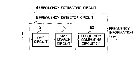
Fig. 1 is a block diagram showing the frequency
estimating circuit that applies when ~f is not necessarily
within an observable range Wl. Fig. 3 is a flow diagram of
the operation of the frequency estimating circuit 4.
There are shown a quantized and sampled input signal 1
(sample value signal), a DFT circuit 2' for converting the
received signal expressed in the time domain into the
frequency domain and for determining the power spectrum of
the received signal, an MAX search circuit 3 for searching
the maximum value of the power spectrum and for determining
the frequency giving the maximum value of the spectrum, a
frequency detector circuit 5 composed of the DFT circuit 2'
and the NIAx search circuit 3, a frequency computing circuit
(1) 60 for estimating the frequency that is a candidate for
0f in view of aliasing based on frequency information fl
determined by the frequency detector circuit 5, and a
frequency estimating circuit 4 comprising the frequency
computing circuit (1) 60 and the frequency detector circuit
5.
The operation of the frequency estimating circuit is
now discussed referring to Figs. 2A and 2B and Fig. 3. Now,
suppose that 0f falls not necessarily within the observation
range. The DFT circuit 2' converts the sampled received
data stream 1 from time-axis signal to a discrete signal on
18
CA 02196468 1999-12-07
a frequency axis (step 102), and derives a power spectrum by
squaring the converted discrete signal (step 103).
The power spectrum output by the DFT circuit 2' is fed
to the MAX search circuit 3. The MAX search circuit 3
searches for the maximum value of the input power spectrum
in power level within i~he observation range W1 (-fs/2 to
+fs/2 in Fig. 2A) (step 104), and determines and outputs the
frequency fl of the spectrum resulting in the maximum value
of the power spectrum (step 105) .
l0 The frequency computing circuit 60 carries out the
following computation 1~o the frequency fl determined by the
MAX search circuit 3, and outputs an estimate value fEST for
Of (step 106) .
fesT = fl + n ~ fs (2)
n : an integer that meats fL <- ( fl + n ~ fs ) <_ fu
The frequency computing circuit 60 outputs a plurality
of frequency information fEST based on the equation (2).
Although fEST estimated as a candidate for the frequency
offset is a sing7_e in nature, the frequency computing
20 circuit 60 is unable to determine n in the equation (2), and
thus estimates and outputs a plurality of candidate
frequencies (fl - 2fs, fl - fs, fl, fl + fs, etc in Fig. 2B) .
Embodiment 2.
Fig. 4 is a block diagram showing an estimating circuit
for two input systems of data streams in which the received
19
~19u~+6u
signal is sampled at different sampling rates. As shown,
designated 61 is a frequency computing circuit (2) for
estimating Of based on two pieces of frequency information
estimated, and DFT circuits 2a, 2b and MAX search circuits
3a, 3b are identical to those described in connection with
the embodiment 1, designated 5 is a frequency detector
circuit comprising DFT circuits 2a, 2b and MAX search
circuits 3a, 3b.
The operation of the frequency estimating circuit is
now discussed referring to Fig. 4 and Fig. 5. Let fsl and
fs2 represent two sampling rates used in producing data
streams from the received signal, and let DFT 1 and DFT 2
represent the respective results that are obtained when DFT
circuits 2a, 2b perform DFT to two input data streams la, lb
sampled.
Fig. 5 shows the resulting DFT, in which ~f is shown as
degenerated fli within the observable range determined by
the sampling rate fsl and f is shown as degenerated f12
within the observable range determined by the sampling rate
fs2. The MAX search circuits 3a, 3b detect maximum power
spectrums within the observable ranges and then outputs
their frequencies as fll, f12.
Of is estimated from each of the detected frequencies
fil, f12 with a view to aliasing as follows.
fEST = fll + nl ' fsl
EST = f 12 + n2 ' fs2
21~5~68
nl, n2: integers, each satisfying
fL <_ (fll + nl ~ fsli f12 + n2 ' fs2) <_ fu
Therefore, the frequency computing circuit (2) 61
determines fggT by solving equation (5) using the frequency
information fll and f12 output from the MAX search circuits
3a, 3b.
fm + W ~ fs~ ~ f~2 + n2 ~ fs2 (5)
Here again in the same way as in the embodiment 1, the
frequency estimating circuit is unable to determine sole nl,
n2, and thus outputs a plurality of candidates.
Embodiment 3.
Fig. 6 is a block diagram showing a frequency
estimating circuit having two input systems, in which the
distribution range of 0f is approximately known, and LPFs
are used to cut off components outside the distribution
range of ~f. As shown, designated 8a and 8b are LPFs having
a transfer function that allows signals within a desired
observation range to pass therethrough, and input signals
la, lb, a frequency detector circuit 5 comprising DFT
circuits 2a, 2b and MAX search circuits 3a, 3b and a
frequency computing circuit (2) 61 are identical to those
described in connection with the embodiment 2.
The operation of the frequency estimating circuit is
now discussed. In the same way as in the embodiment 2, ~f
21
CA 02196468 1999-12-07
is sought within the observable range, and the distribution
range of Of is within the pass bandwidth of the Low Pass
Filter (LPF), and the condition of nl, n2 in equations (3)
and (4) is as fo:Llows:
nl, nz . integers, each satisfying ( ~ fEST ~ 5 pass
bandwidth of LPF;
Therefore, 1=he frequency computing circuit (2) 61
determines n,, nz that satisfy this condition, estimates Of,
and outputs an e;~timat~~ value as the frequency information
f EST
Two LPFs 8a,. 8b may have different pass bandwidths.
Embodiment 4.
Fig. 7 is a block diagram showing an estimating circuit
which estimates j=requency by introducing a time difference
between two input. systems. In this case, discussed herein
is an example of a selector 30 as a time difference circuit
is incorporated in a frequency estimating circuit of the
embodiment 2.
Fig. 8 is a diagram illustrating the operation of the
circuit with a tome difference introduced between two input
systems, and Fig., 9 is a flow diagram showing the operation.
Referring to Fig., 7, designated 30 is the selector included
to introduce the time difference between the two input
systems, and the frequency detector circuit 5 and the
frequency computing circuit (2) 61 remain identical to those
described in connection with the embodiment 2.
22
Z1 ~c~~G~
The operation of the frequency estimating circuit is
discussed referring to Fig. 8 to Fig. 9. Although, in the
embodiments 2 and 3, the received signal is sampled at
different sampling rates, both data processed by the DFT
circuit 2'a and the MAX search circuit 3a and data processed
by the DFT circuit 2'b and the MAX search circuit 3b are
originated at the same time. If ~f is not time variant, and
not varying while data is sampled, a time difference may be
introduced between two input data streams.
The selector 30 selects the DFT circuit 2'a and MAX
search circuit 3a (step 110), and fll is derived from a data
stream la (step 111).
The selector 30 then selects the DFT circuit 2'b and
MAX search circuit 3b (step 112), and fit is derived from a
data stream lb (step 113). Fig. 8 shows one example, in
which a time difference is introduced in decimation of input
data streams to the DFT circuits in this embodiment.
By introducing the time difference between the input
data streams, correlation between noises of two input data
streams is smaller than the correlation that is derived from
the same received signal, the influence of noise is reduced,
erroneous detection is reduced, and estimation of Of is
improved.
Embodiment 5.
23
''' 2196468
Fig. 10 is a b~.ock diagram showing a frequency
estimating circuit that produces a new data stream by
extracting data at regular intervals from a quantized and
sampled data stream and thus estimates frequency.
Designated 41 is a decimating circuit. The decimating
circuit 41 extracts data, at regular intervals of a samples
from a sample count N in the input data stream l, and
produces a new data stream 1'. Herein, a is a factor of the
sample count N. The rest of the organization of this
embodiment is identical to that of the preceding
embodiments.
The organization constructed of the decimating circuit
4i, DFT circuit 2' and MAX search circuit is referred to as
a decimating and frequency detector circuit 51.
The operation of the frequency estimating circuit is
discussed referring to Fig. 11 and Fig. 12.
The decimating circuit (1) 41 extracts data at regular
intervals of a samples from the sample count N in the data
stream 1 that is sampled at a sampling period TS, thereby
producing a new data stream 1' having a sampling period of
aTs (step 115).
The DFT circuit 2' converts the new data stream 1' from
time-axis signal to frequency-axis signal (step 116), and
squares the frequency-axis signal to derive a power spectrum
(step 103). The MAX search circuit 3 searches for the power
24
219~46~
spectrum having a maximum level and determines the frequency
f2 of the maximum power spectrum (step 117).
Fig. 11 shows two cases: in one case, the new data
stream 1' is produced by extracting data on a per a samples
basis from the data stream 1 and is then subjected to DFT,
and in the other case, the data stream 1 is directly
subjected to DFT.
Now consider N samples in the data stream 1 sampled at
a sampling period Ts. Data is extracted on a per a samples
basis (a is a factor of N) from the data stream 1 to produce
the data stream 1' having a sampling period equal to the
original sampling period times a, the data stream 1' is
time-axis to frequency-axis converted, and the result is
compared with the result derived from the data stream 1 that
is directly time-axis to frequency-axis converted, showing
that the observation range for the data stream 1' is 1/a
times the observation range for the data stream 1. The
frequency interval from the frequency-axis converted data
stream 1' remains identical to that from the frequency-axis
converted data stream 1.
Fig. 13 illustrates a more specific example with a = 4.
Although through the decimation process, the observation
range of the data stream 1' is 1/4 the observation range of
the data stream 1 as shown, ~f is estimated within a range
equivalent to the observation range of the data stream 1 by
considering aliasing in the same way as in the embodiment 1.
CA 02196468 1999-12-07
Specifically, let fz represent the frequency detected
by the MAX search circuit 3, and fEST is expressed as
follows.
fEST = fz + -n ~ fs/~a (5)
n: an integer satisfying (fL <_ f2 + n ~ fs/a <_ f~)
A frequency computing circuit 62 is unable to determine n in
the equation (5), and thus outputs a plurality of
candidates.
Embodiment 6.
Fig. 14 is a block diagram showing a frequency
estimating circuit having an LPF, in which the distribution
range of Of is approximately known, and the LPF is used to
cut off components outside the distribution range of 0f. As
shown, a data stream 1, a decimating and frequency detector
circuit 51, and a frequency computing circuit (3) 62 remain
identical to those described in connection with the
embodiment 5, and the LPF 8 is identical to that described
in connection with the embodiment S.
The operation of the frequency estimating circuit is
now discussed. The frequency computing circuit (3) 62
estimates 0f using f2 in the same way as in the embodiment
5, the condition for n in equation (5) is as follows.
n: an integer satisfying (~fesT~ <_ pass bandwidth of
LPF)
26
CA 02196468 1999-12-07
Thus, n satisfying the above condition is determined,
and fEST is output as frequency information. Here again, as
in the embodiment l, the frequency computing circuit (3) 62
is unable to determine n in equation (5), and thus outputs a
plurality of candidates.
Embodiment 7.
Fig. 15 is a block diagram of a frequency estimating
circuit, in which the input data stream is decimated by two
systems of decimating circuit for frequency estimation. In
the figure, an input data stream 1 and a decimating and
frequency detector circuit 51 are identical to those
described in connection with the preceding embodiment.
Designated 61 is a frequency computing circuit that performs
computation based on the output from the decimating and
frequency detect~ar circuit 51.
The organization shown here in the figure is referred
to as a multi-input frequency estimating circuit.
The operati~an of the estimating circuit is discussed
referring to Fig. 16. The decimating and frequency detector
circuit 51 extracts, from the data stream l, data at
intervals p and q, both of which are mutually prime, in
order to produce two new data streams 2 (hereinafter
referred to as data stream la and data stream lb) (step
121 ) .
27
"~- ~ 21 ~ c~ ~
The data stream la and data stream lb are subjected to
DFT, and frequency corresponding to ~f within each of
frequency observable ranges is detected from the maximum
value of the spectrum (step 122).
Let fzl and fzz represent the detected frequencies, and
the estimated value of Of is expressed in consideration of
aliasing as follows.
fssT = fzi + W ' fs/p (6)
fesT = fz2 + n2 ' f9/q
nl, nz: integers, each satisfying (fz <_ fESr S f")
Of is estimated by determining nl, n2 that satisfy
equation (7).
fzi + ni ' f~/p = fez + n2 ' fs/q (7)
The frequency computing circuit (2) 61 solves the
equation (7) using fzl, fzz. to estimates Af, and outputs an
estimated value as frequency information fEST (step 123).
Here in the embodiment 1, the frequency estimating circuit
is unable to determine nl, n2 in the equation (7), and
outputs a plurality of candidates.
Embodiment 8.
Fig. 17 is a block diagram showing a multi-input
frequency estimating circuit 28 having an LPF 8, in which
the distribution range of ~f is approximately known, and the
28
219~4~~
LPF 8 is used to cut off components outside the distribution
range of ~f.
The operation of the multi-input frequency estimating
circuit is now discussed. The frequency computing circuit
(2) 61 estimates ef using equation (7) in the same manner as
in the embodiment 7, and the condition for nl, n2 is as
follows.
nl, nz : integers, each satisfying ( ~ fEST ~ <_ pass
bandwidth of LPF)
20 Fig. 18 shows one specific example. Data is extracted
from the data stream 1 at intervals of 3 samples and 4
samples to produce two new data streams, which are then
subjected to DFT. Since frequency observable ranges are 1/3
and 1/4 the full data (frequency resolution remains
unchanged), observation ranges are (f~ <_ 20 Hz, ~f~ 5 15 Hz
if the observation range W1 is ~f~ 5 60 Hz with the pass
bandwidth of the LPF being the observation range W1.
Suppose that' estimated frequencies~are
f21 = 15 Hz
20 f22 = - 5 Hz
then, equation (7) is
15 + nl ~ 40 = - 5 + n2 ~ 30
By solving equation (7), the frequency computing circuit (2)
61 gives
nl = 1
29
''" 219646
n2 = 2
thus,
fES~ = 55 Hz
Embodiment 9.
Fig. 19 is a block diagram showing the embodiment
according to the eighth invention of the frequency
estimating circuit, Fig. 20 is a diagram illustrating its
operation, and Fig. 21 is a flow diagram showing the
operation.
In Fig. 19, designated 70 is a secondary frequency
detector circuit (1) composed of a DFT circuit 2' and an MAX
search circuit 3, and designated 63 is a frequency computing
circuit (4) that estimates Of within an observation range 1
using the frequency information output by a decimating and
frequency detector circuit and outputs a plurality pieces of
frequency information.
An input data stream 1, a DFT circuit 2', an MAX search
circuit 3 and a frequency computing circuit (1) 60 are
identical to those described in connection with the
embodiment l, and the decimating and frequency detector
circuit 51 is identical to that described in connection with
the embodiment 5.
The operation of the frequency estimating circuit is
discussed referring to Fig. 19 to Fig. 21. The input data
stream 1 is decimated by the decimating and frequency
2~ 9468
detector circuit 51 at predetermined intervals of a samples
to produce a data stream 1' (step 115), the data stream 1'
is time-axis to frequency axis converted, the frequency at
the maximum level in a spectrum is determined and then
output as f2 (step 118). Based on f2, the frequency
computing circuit 63 performs computation and outputs
frequency information as fEST (step 120).
There remain candidates within a frequency range W1.
Since the range outside the frequency range W1 is now going
l0 to be observed taking advantage of aliasing, the number of
the candidates of ~f is a x n if a range equal to n times
the observation range W1 is considered (n: an integer). The
number of candidates is reduced in the following technique.
If the data stream 1 is used, ~f exists Within the
observation range 1 and can be estimated.
Thus, a plurality of f~sr are first determined in the
same manner as in the embodiment 2. Fig. 20 shows an
example with a = 4. The DFT circuit 2' performs DFT to the
data stream 1 again but at four frequencies only
2o corresponding to ~f based on fEST output from the frequency
computing circuit (4) 63 to determine the power spectrums.
The MAX search circuit 3 searches the maximum one in the
four power spectrums; and then outputs the frequency
corresponding to the maximum power spectrum (second from the
leftmost one in Fig. 20). This spectrum has a frequency of
f,. In this way, the use of the secondary frequency
31
CA 02196468 1999-12-07
detector circuit (1) 70 reduces the number of candidates to
1/a.
The frequency computing circuit (1) 60 as a succeeding
stage performs c~~mputation of equation (5) using fl,
estimates 0f over a range inclusive of the range outside'the
observation range Wl, and outputs an estimated value as fEST
(step 106). Here again, as already described, the frequency
estimating circuit is unable to determine n in equation (5),
and thus outputs a plurality of candidates.
Embodiment 10.
Fig. 22 is a block diagram showing a frequency
estimating circuit having an LPF, in which the distribution
range of 0f is approximately known, and the LPF is used to
cut off componeni~s outside the distribution range of ~f.
Fig. 22 is a block diagram of the embodiment 6 of the
frequency estimai~ing circuit.
In the figure, the LPF 8 is identical to that described
with reference to the embodiment 3, and an input data stream
1, a decimating and frequency detector circuit 51, a
frequency comput_Lng circuit (1) 60, a frequency computing
circuit (4) 63 and a secondary frequency detector circuit
(1) 70 are identical to those described in connection with
the embodiment 9.,
The operation of the frequency estimating circuit is
discussed. Since the distribution range of ~f is
32
CA 02196468 1999-12-07
approximately known, the distribution range of 4f is within
the pass bandwidth of the LPF. Therefore, the computation
of the frequency computing circuit (1) 60 is simply
performed within the pass bandwidth of LPF 8. Specifically,
the frequency computing circuit (1) 60 computes and outputs
frequency information fEST with the condition for n as
follows.
n: an integer satisfying (~fEST~ <_ Pass bandwidth of
LPF)
Embodiment 11.
Fig. 23 is a block diagram showing the frequency
detector circuit (2) according to the emibodiment 11 of the
present invention. As shown, designated 44 is a decimating
circuit (2) that extracts data from a data stream 1 so that
the sample count is 1/b times that of the data stream 1 to
produce a data stream 1", and designated 21 is a frequency
detector circuit (2) composed of the decimating circuit (2)
44 and a frequency detector circuit 5. The frequency
detector circuit 5 is identical to that described in
connection with the embodiment 1.
Referring to Fig. 24, the operation of the frequency
detector circuit is discussed. The decimating circuit (2)
44 extracts data from the data stream 1 consecutively so
that the sample count is 1/b times the data stream 1 and
thus produces the data stream 1". The frequency detector
33
circuit 5 performs time-axis to frequency-axis conversion to
the data stream 1", determines the frequency of the maximum
value power spectrum to result in ~f, and output an
estimated value as f3.
Fig. 24 is a comparison diagram that compares the
result of DFT operation carried out to the data stream i
with the result of DFT operation carried out to the data
stream 1" that is derived by decimating the data stream 1 to
for it to have the sample count 1/b times the data stream 1.
In Fig. 24, (a) shows the data stream 1 having N
samples with a sampling period of Ts. (b) shows the data
stream 1" that is obtained by consecutively decimating the
data stream 1 to be 1/b times the data stream 1. (c) and
(d) show the results of DFT operations that have been
carried out to the data stream 1 and the data stream i".
These results are attributed to the characteristic of DFT.
The DFT result of the data stream 1" is 1/Ts times the
DFT result of the data stream 1 in terms of observation
range, but the frequency.interval of the DFT result of the
data stream 1" is b/NTs, which is b times that of the data
stream 1.
Therefore, although the decimation operation reduces
the computational load, the frequency detector circuit 5
presents a lower frequency estimation accuracy in the DFT
result of the data stream 1" than in the DFT result of the
data stream 1, and the frequency detector circuit (2) 21 in
34
219~~~8
this embodiment is suitable for approximate estimation of
frequency.
Embodiment 12.
Fig. 25 is a block diagram showing the frequency
detector circuit according to the embodiment 12 of the
present invention. There are shown a decimating circuit (2)
44, a frequency detector circuit 5, and a secondary
frequency detector (2) 71. The organization comprising
30 these component is referred to as a frequency detector
circuit (3) 22.
Fig. 26 illustrates the operation of the frequency
detector circuit, and Fig. 27 is a flow diagram of the
operation. In Fig. 25, designated 71 is the secondary
frequency detector circuit (2) 71 composed of the DFT
circuit 2' and MAX search circuit 3, and the decimating
circuit (2) 44 and the frequency detector circuit 5 are
identical to those described in connection with the
embodiment 11.
20 Referring to Fig. 25 to Fig. 27, the operation of the
frequency detector circuit is discussed. The decimating
circuit (2) 44 decimates the data stream 1 by 1/b times to
produce a data stream 1" in the same manner as in the
embodiment 11 (step 127). The frequency detector circuit 5
performs DFT to the data stream 1", determines the frequency
of the maximum power level spectrum, and outputs frequency
information f3 (step 128).
The secondary frequency estimating circuit (2) 71
performs DFT to f3 that is estimated based on the DFT result
of the data stream 1" and to the data stream 1 in the
vicinity of f3, and outputs the result of frequency
estimation as frequency information fEST (step 129).
Fig. 26 shows an example of operation with b = 4.
Since as shown, the frequency interval is quadrupled as a
l0 result of decimation in the DFT result by the frequency
detector circuit 5, the secondary frequency detector circuit
(2) 71 performs afresh frequency estimation in the data
stream 1 in frequencies in the vicinity of f3 (a total of 9
frequencies f3 - 1 ~ f3 + 1 in Fig. 26). In the secondary
estimation, the frequency interval becomes quartered, and
the estimation offers a higher accuracy compared with the
estimation of the data stream 1".
Embodiment 13.
20 Fig. 28 is a block diagram of the frequency estimating
circuit in which the preceding embodiment 12 is incorporated
in the embodiment 1. There are shown a input data stream l,
a frequency detector circuit (3) 22 and a frequency
computing circuit (1) 60. Fig. 29 is a flow diagram showing
the operation of the frequency estimating circuit.
36
w.. 219r~4~~
The operation of the frequency estimating circuit is
now discussed. The frequency detector circuit (3) 22
produces a data stream 1" by decimating the input data
stream 1 so that the data stream 1" has a sample count lib
times the sample count N in the input data stream 1 (step
127), the data stream 1" is then subjected to time-axis to
frequency-axis conversion, the frequency of maximum power
level spectrum is~determined and thus f3 is determined (step
128) .
DFT is again performed to only the vicinity of f3 and
frequency information is output as fESx (step 129). The
frequency computing circuit (1) 60 estimates Af in view of
aliasing in the same manner as in the embodiment 1, and
frequency information fEST is estimated (step 130).
Embodiment 14.
Fig. 30 is a block diagram showing the frequency
estimating circuit of one embodiment of the present
invention. Described herein is the embodiment in which above
described frequency detector circuit described in connection
with the embodiment 11 or the embodiment 12 is incorporated
in the frequency estimating circuit described in connection
with the embodiment 10.
As shown, the input data stream 1, frequency computing
circuit (1) 60, frequency estimating circuit (4) 63 and
secondary frequency detector circuit (2) 71 are identical to
37
'~.
those described in connection with the embodiment 10, the
decimating circuit (1) 41 is identical to that described in
connection with the embodiment 5, and the frequency detector
circuit 5 and decimating circuit (2) 44 are identical to
those described in connection with the embodiment 11.
The operation of this embodiment is discussed referring
to Fig. 30. By allowing the input data stream 1 to pass
through the decimating circuit (1) 41 and the decimating
circuit (2) 44, a new data stream is produced. When the new
data stream is subjected to DFT, both characteristic 1 and
characteristic 2 of DFT already described are applied to the
DFT result, and when the frequency estimated by the
frequency detector circuit 5 is compared with the DFT result
of the input data stream 1, the computational load involved
is smaller, the estimated f is degenerated into the
observation range W2 and its discrimination is poor.
For this reason, the secondary frequency detector
circuit (2) 71 performs afresh frequency estimation using
the input data stream 1 in the- vicinity of the frequency
estimated by the frequency computing circuit (4) 63, and
then estimates frequency information fEST. The order of
arrangement is not important in that the decimating circuit
(1) 41 may be arranged ahead of the decimating circuit (2)
44 and vice versa, or both circuits may perform decimation
concurrently.
38
' 21 ~~~~8
..... .
Embodiment 15.
Fig. 31 is a block diagram showing the frequency
estimating circuit of one embodiment of the present
invention. Described herein is the embodiment in which the
secondary frequency detector circuit described in connection
with the embodiment 12 is incorporated in the frequency
estimating the embodiment 7.
As shown, a decimating and frequency detector circuit
51, a frequency computing circuit frequency (2) ~3, and a
multi-input frequency estimating circuit 2'8 are identical
to those described in the embodiment 7, the secondary
frequency estimating circuit (2) 71 is identical to that
described in the embodiment 12, and the frequency computing
circuit (1) 4 is identical to that described in the
embodiment 4.
The operation of the frequency estimating circuit is
now discussed referring to Fig. 31. Two decimating and
frequency detector circuits 51 decimate the input data
stream 1 at two different intervals which are mutually prime
to produce data streams 2. Each data stream is subjected to
time-axis to frequency-axis conversion, and frequencies in
the vicinity of the frequencies of maximum power level
spectrums in the data spectrums 2 are output and frequencies
corresponding to several power spectrums from the power
spectrum of highest level, as f21 and f22, are output. The
39
~~9~~~8
frequency computing circuit 61 computes equation (7) using
f21, fez, and outputs a plurality of frequency information fl.
In response to the time-axis to frequency-axis
conversion of the input data stream 1, the secondary
frequency estimating circuit (2) 71 searches power spectrums
in the vicinity of the frequency information fl from the
frequency-axis computing circuit 61 to find and then output
the frequency of the maximum value power spectrum. The
frequency computing circuit (1) 60 computes equation (2)
based on the frequency information to estimate frequency
outside the observation range l, and then outputs the
estimated frequency information fEST.
Embodiment 16.
Fig. 32 shows the embodiment which is constructed of
the preceding embodiment with an LPF 8 added, wherein its
frequency offset is approximately known.
The operation of this embodiment is now discussed
referring to Fig. 32. The operation of the-multi-input
frequency detector circuit 28 and secondary frequency
detector circuit (2) 71 is identical to that of the
preceding embodiment. In this embodiment, since the
distribution range of the carrier is approximately known,
the frequency estimating circuit results in an acceptable
frequency estimation within the observation range that is
CA 02196468 1999-12-07
determined by a sampling period at which the input data
stream 1 is samf~led.
The frequency computing circuit (1) computes equation
(2) based on the output information from the mufti-input
frequency detector circuit 28 with the condition for n a-s
follows and outputs fESn
n: an integer satisfying (~feST~ <_ Pass bandwidth of LPF)
Embodiment 17.
Fig. 33 is a block diagram of the frequency detector
circuit having frequency interpolation circuit therewithin.
Figure shows the embodiment in which a frequency
interpolation circuit is incorporated in the detector
circuit of the embodiment 1.
The operation of this embodiment is now discussed. The
DFT circuit 2' and the: MAX search circuit 3 perform
frequency estimation using the power spectrum of the input
data stream 1. Although the frequency that gives a maximum
power spectrum is conventionally output as frequency
information fl, l~he frequency that can be observed as a
result of DFT is discrete value, and estimation error takes
place is Of fails to agree with the frequency point of
observation.
For this reason, to estimate frequency at a higher
accuracy level, the output frequency of the MAX search
circuit 3 derived from the maximum power spectrum is
41
CA 02196468 1999-12-07
interpolated. A:~ an e:~cample of interpolation, Lagrange's
secondary interpolation is used herein. Fig. 34 shows the
operation of interpolation. In Fig. 34, it is assumed that
fl is at a maximum.
A frequency interpolation circuit 20 interpolates
between three power va:Lues, a power value at fl and power
values at two points (fl - l, fl + 1) adjacent to fl, and
then estimates the frequency that is supposed to give the
true peak power ~Talue. The frequency interpolation circuit
20 performs interpolation in this way, and outputs afresh as
fl the frequency resulting from interpolation.
Embodiment 18
Fig. 35 is a blocl~ diagram of an AFC circuit as the
embodiment 11 according to the eleventh invention in which
the frequency estimating circuit is incorporated. As shown,
an input data steam 1 and a frequency estimating circuit 4
are identical to those described in connection with the
embodiment 1. There a:re also shown a frequency correction
block 7 for corrE:cting a received signal and a determining
circuit 29 for cieterm:ining synchronization.
The operation of this embodiment is now discussed
referring to the flow diagram in Fig. 36.
The frequency est:imating circuit 4 time-axis to
frequency-axis converts the input data stream 1 to determine
a power spectrum, and determines the frequency corresponding
42
1
' 219646
,..
to the maximum power, computes a predetermined equation
(equation (2) in this case) to estimate ~f, and outputs a
plurality of frequency information fEST (step 132).
The frequency correction block 7 removes ~f from the
input data stream 1 using the plurality of frequency
information fgST (step 133) to produce a plurality of
demodulated data streams. The determining circuit 2'9
determines the synchronization of frequency using the
plurality of demodulated data streams output from the
l0 frequency correction block (step 134), and outputs its
determination result to the frequency correction block.
The frequency correction block 7 is now discussed
further in detail. Fig. 37 shows an example of the
organization of the frequency correction block 7. fssr -
converter 81 determines ef based on fEST output by the
frequency estimating circuit 4. A reversed phase generator
circuit 82 determines reversed phase angle of rotation at
each sampling point using 0f determined by the fEST
converter 81.
20 A phase reverse rotating circuit 83 removes a quantity
of phase change from the received data stream based on the
input data stream 1 and the angle of rotation corresponding
to each data. ~f is removed in this way. As data to be
demodulated, the received signal having no Af is output to
43
' 2I 9646
the determining circuit 29 and a demodulator block at the
next stage.
Next, 0f is removed from the received signal 1 based on
a plurality of frequency information fEST to produce a
plurality of data streams. One method of removing Of is
discussed next.
Since the received signal is a pilot signal (non-
modulated signal), the phase of the received signal is 0
with Af= 0 regardless of sampling timing (Ts). If ~f ~ 0,
i0 however, the phase of the received signal varies with time
as shown in Fig. 39, and the quantity of phase change O8 is
08 = ~f x 360 x TS
. Phase change per sample (degrees)
0f . Frequency offset estimated (Hz)
T, . Sampling period (seconds)
Since the phase change is determined by determining
using the frequency information fEST estimated by the
frequency estimating circuit anti the sampling period TS, the
phase at each symbol becomes 0 if the phase change is fed
20 back at each symbol. The frequency correction block 7 thus
determines O8 based on fEST estimated by the frequency
estimating circuit 4. A complex multiplier is used to
correct the phase at each sampling point as shown in Fig.
40. The data stream thus corrected is output to the later
stage.
44
CA 02196468 1999-12-07
One example of do=termining method is now discussed. A
known pattern detection such as Unique Word (UW) detection is
performed. Since the distribution range of Of is generally
finite (fL _< ~f s f") , n in equation (2) is a finite number.
Suppose that the number of a plurality of frequency
information output by t:he frequency estimating circuit 4 is K,
and that these pieces of frequency information are fgSTl ~ fESTK.
The frequen~~y correction block 7 produces a demodulated
data stream by removing Of corresponding to fESTl from the
received data, a:ad then outputs it to the determining
circuit 29. The determining circuit 29 detects a known
pattern used in the system such as UW in the demodulated
data stream. When no known pattern is detected, the
determining circuit 29 outputs no-detection signal to the
frequency correction block 7.
Receiving the no-detection signal, the frequency
correction block 7 outputs a demodulated data stream that is
produced by removing Of corresponding to next frequency
information fgST2 from t=he received signal. This process is
repeated until a known pattern is detected.
When the known pattern is detected, the determining
circuit 29 outputs a detected signal to the frequency
correction block 7. When the frequency correction block 7
receives the detected signal, it fixes a frequency to be
corrected, with a frequency corresponding to it, and
21 ~6~+~
corrects with the frequency thereafter. If no known pattern
is detected in connection of all K candidates, the AFC
operation is regarded as failed.
The prior art AFC circuit can estimate ~f only within
the observable range. Thus, the prior art AFC suffers the
disadvantage that it cannot perform frequency estimation
when Of is large and outside the observable range even with
no influence of noise. According to the present invention,
however, the observable range is infinite, and 0f is
30 estimated without fail with no influence of noise or the
like, and a highly accurate and reliable synchronization is
established.
Alternative embodiment i
In the embodiment 9 and embodiment 10, the data stream
1' is used to estimate ~f within the observation range W2,
and a plurality of candidates for ~f within the observation
range W1 are estimated by the frequency computing circuit
(1) 60, DFT is performed only these plurality of frequencies
20 by the secondary frequency estimating circuit (1) 70, and
fesT within the observation range W1 is determined, and the
use of the characteristic 1 of DFT is on condition that a
must be a factor of sample count N.
Described herein is the embodiment in which a is not a
factor of the sample count N.
46
- 219646
Fig. 41 shows the DFT result when a is not a factor of
the sample count N. The operation of the embodiment is now
discussed referring to Fig. 41. When a is not a factor of
the sample count N, N cannot be divided by a, and if data
extraction is performed from the first sample at intervals
of a samples, d data remains at the end of the data stream
(d < a), an observation time length for DFT is shortened,
and the observation~time length is expressed by equation
(g) .
N' ~ Ts = (N - d)~ Ts (8)
As a result, the frequency interval becomes longer, and
it can be expressed by equation (9) as follows.
1 ~ (jW ~ Ts) - 1 /~ (N - d) ' Ts~ (g)
In this way, since the frequency point of observation
with the data stream 1' subjected to DFT is different from
the frequency point of observation with the data stream 1
subjected to DFT, the secondary frequency estimating circuit
(1) 70 cannot observe the frequency that corresponds to the
estimated value fEST with the data stream 1'. In such a
case, therefore, the secondary frequency estimating circuit
(1) 70 performs DFT to the data stream 1 at a plurality of
points of observation in the vicinity of fEST.
47
23 96468
Alternative embodiment 2
In the embodiment 7 and embodiment 8, as well, the use
of the characteristic 1 of DFT is on condition that a is a
factor of the sample count N.
Described herein is the embodiment in which a is not a
factor of the sample count N. When a is not a factor of the
sample count N in both decimating circuits 41 or one of
decimating circuits 41, the frequency interval is expressed
by equation (9), estimated values f21, fzz from two
decimating and frequency detector circuits are ones over
different frequency intervals, and thus nl, n2 satisfying
equation (5) do not exist.
In such a case, the frequency computing circuit (2) 63
uses equation (10) modified from equation (5) to determine
nl. n2.
f21 + nl f/p °. fz2 + n2 ' f/q (10)
Alternative embodiment 3
In the embodiment 18, the AFC is arranged in the form
of feedforward type, but alternatively, it may be arranged
in the form of feedback type.
Such an arrangement is shown in Fig. 42.
In Fig. 42, a mixer 18 multiplies the output from an
oscillator for down-conversion (hereinafter referred to as
D/C) by a received signal input to remove ~f from the
received signal, and a D/C oscillator 19 outputs the
frequency corresponding to the frequency information fEST
48
219646
output by a frequency estimating circuit 4, and the
frequency estimating circuit 4 and a determining circuit 29
are identical to those described in connection with the
embodiment 18.
In the same way as in the embodiment 18, the frequency
estimating circuit 9 estimates Of, and outputs a plurality
of frequency information. The D/C oscillator 19 outputs the
frequency corresponding to the frequency information, and
the mixer 18 multiplies the output from the D/C oscillator
19 by the input received signal to remove Af from the
received signal. The determining circuit 29 determines the
synchronization of frequency using the demodulated data
stream output by the mixer 18, and outputs its determination
result.
Thereafter, the determination of the synchronization of
frequency are performed in the same way as in the embodiment
18.
Alternative embodiment 4
In the frequency estimation in the embodiment 2 .-.-
embodiment 4, embodiment 7, embodiment 8, embodiment 15 and
embodiment 1&, two processings are performed, and increasing
the number of processings may reduce detection error and
allow 0f to be estimated at a good accuracy level.
Although in these embodiments, processings are
parallel, a single decimating and frequency estimating
49
2~ 96~+6~u
circuit may be allowed to perform a plurality of processings
using buffers if processing time presents no problem. In
this way, the decimating and frequency estimating circuit
may be of a single arrangement, and its construction is
simplified.
Alternative embodiment 5
The LPF is provided to remove components outside the
band of the signal in the embodiment 3, embodiment 6,
embodiment 8, embodiment 10, embodiment 14 and embodiment
16, but such an LPF is needless if the aliasing noise and
noise within the desired observation range are negligibly
low (with an excellent S/N ratio). Such an arrangement
simplifies the construction of each of the above
embodiments.
Alternative embodiment 6
In the embodiment 18, the frequency correction process
and the determining process are repeated to fESTl ~ fESTK until
a known pattern is detected, and if the distribution of
frequency offset 0f has any particular feature, the
processes may be carried out in the order that is suited to
the feature.
For example, the distribution of Of is in the vicinity
of 0, the processing may be first performed to frequencies
corresponding to fEST close to 0, and then fEST may be
2196468
selected in the order of farther away from 0 for processing.
In this way, the time to search for ~f is shortened, and
thus the time to establish synchronization is accordingly
shortened.
Alternative embodiment 7
In the embodiment 18, once a known pattern is detected,
the remaining candidates are not subjected to the frequency
correction process and the determining process. Since there
is a possibility of detection error under the influence of
noise, the frequency correction process and the determining
process may be performed to the remaining candidates even if
the known pattern is detected at a frequency.
When the known pattern is found in a single candidate
only, the frequency correction block 7, upon receiving the
detected signal, fixes a frequency to be corrected, with a
frequency corresponding to it, and corrects thereafter with
the frequency. If the known pattern is found in a plurality
of candidates, the determination of the frequency may be
left to the demodulator block at the succeeding stage. In
this way, detection error due to noise or the like is
prevented, and ~f is estimated at an improved accuracy.
Although this embodiment has been described in
connection with the AFC circuit into which the embodiment 1
is incorporated, detection error due to noise or the like
may be controlled if the frequency estimating circuit in the
51
19046
embodiments 2 through 17 is employed, and ~f is equally
estimated at an improved accuracy.
As described above, according to the present invention,
time-axis to frequency-axis conversion is performed and
frequency information is estimated based on a plurality of
candidates of 11f from the frequencies of the maximum power
spectrum, and thus, the frequencies in a conventionally
unobservable range toutside the observable range) can be
observed, and a wider frequency range is observed with a
data quantity remaining unchanged from that in the prior art
system.
Frequency estimation is performed in different
observation ranges by using a plurality of data streams
sampled at different sampling rates, and thus Of in a
conventionally observable range is estimated within the
observation range with a smaller quantity of data by taking
into consideration aliasing in a plurality of frequency
information, and furthermore, with aliasing considered, a
wider frequency range is observed with the data quantity
remaining unchanged from that in the prior system.
Since, in the course of frequency estimation, a time
difference is introduced between two data streams to be used
in frequency estimation, correlation of noise between the
two data streams is small compared with that resulting from
the decimation of the same data stream l, and the influence
52
' ~-- ~ 219~46c~
of noise is reduced, the occurrence of detection error is
lessened, and a more accurate ~f is thus estimated.
By allowing the decimating circuit to decimate the
input data stream in the frequency estimation, ~f is
estimated within the observation range with a smaller
quantity of data than that in the prior art system, and
further the same advantage as the first invention is
obtained-taking into consideration aliasing.
As described above, a plurality of decimating circuits
are used to performed frequency estimation in different
frequency ranges and aliasing is considered in a plurality
of frequency information, and thus f is estimated within the
observation range with a smaller quantity of data than that
in the prior art system, and further the same advantage as
the first invention is obtained taking into consideration
aliasing.
Furthermore, as described above, the same advantage as
the fourth invention is provided; and, further all data is
used to perform afresh frequency estimation and thus a
single frequency candidate is obtained. In view of
aliasinq, the same advantage as the first invention is
provided.
Moreover, as described above, the use of the decimating
circuit allows rough frequency estimation with a smaller
data quantity.
53
- ~1 ~~6~68
Frequency estimation is performed with a smaller data
quantity after the data stream is decimated, all data is
afresh subjected to frequency estimation, and thus a high
discrimination frequency estimation is performed with a
small processing quantity.
Since the frequency detection result from the frequency
estimating circuit is frequency interpolated, frequency
estimation is performed at a high accuracy level.
In the AFC circuit that demodulates the received
signal, the input data stream, a plurality of estimatere
used to determine synchronization, and frequency estimation
is performed in a wide range and a highly accurate and
reliable synchronization is established.
54