Note : Les descriptions sont présentées dans la langue officielle dans laquelle elles ont été soumises.
2 1 97 1 96
~096~5521
FIELD OF THE INVENTION
The present invention relates to radiation detectors.
APPARAT~S, SYSTEM AND METHOD FOR GAMMARAY AND
X-RAY DETECTION
~ACKGROUND OF THE INVENTION
Semiconductors as radiation detectors are discussed in
G. F. Knoll, Radiation ~eteCtiQn ~n~ Mp~snrementr John Wiley and
Sons, Second Edition, 1989, pp. 349. Knoll defines an Ohmic
contact as l'a nonrectifying electrode through which charges of
either sign can flow freely. If two Ohmic contacts are fitted
on opposite faces of a slab of semiconductor and connected to a
detection circuit, the equilibrium charge carrier concentrations
in the semiconductor will be maintained. If an electron or hole
is collected at one electrode, the same carrier species is
injected at the opposite electrode to maintain the e~uilibrium
concentrations in the semiconductor."
Regarding semiconductor diode detectors, Knoll states
on page 350: "The steady-state leakage currents that are observed
using Ohmic contacts are too high, even with the highest resis-
tivity material available.... Instead, noninjecting or blocking
electrodes are universally employed to reduce the magnitude of
the current through the bulk of the semiconductor. If blocking
electrodes are used, charge carriers initially removed by the
application of an electric field are not replaced at the opposite
electrode, and their overall concentration within the semiconduc-
~Ub~l~lu~t SHEEr (RUIE ~6~
21 97l 96
W096/05521 ~ 't~C5
tor will drop after application of an electric field."
Possible use of cadmium telluride for detection ofpulsed x-rays in medical tomography is described in E. N.
Arkad'eva et al, Sov. Phys. Tech. Phys. 26(9), September 1981,
pp. 1122-1125. Arkad'eva et al state on pp. 1123-1124: "We used
an M-P-M structure with osmium contacts as a detector based on
these crystals... The current from the x-ray excitation (the
photocurrent) at the detector may be written in the steady-state
regime in the form j=e~ ~nE, where e is the electronic charge,
is the carrier mobility, E is the electric field, ~ n is the
concentration of photocarriers created by the light, ~ n=~k ~ I,
where ~ is the quantum yield (~ = 1), k is the absorption
coefficient for x-rays in the transducer, ~ is the carrier
lifetime, and I is the radiation intensity."
Fig. 2 of Arkad'eva et al graphs x-ray absorption at
various energies for cadmium telluride crystals of thickness 1 mm
(curve 1) and 2 mm (curve 2).
Fig. 3 of Arkad'eva et al graphs dark current (curves 1
and 2) and photocurrent (curves 1' and 2') as a function of the
voltage across the device in continuous wave operation.
A method of manufacture for a high-resistance n-type
CdTe crystal is described in K. ~anio, et al, IEEE Trans. Nucl.
sci., NS21, 315, 1974.
A method for attaching contacts to the CdTe crystal is
described in R. E. Braithwaite et al, solid State Electron., 23,
1091, 1980.
A preferred method for producing p-type HgTe is de-
SUBSTITUTE SHEET (RULE 26)
2t97196 . ll~, J~5;'
~ WO96/05521
scrlbed in E. Janik and R. Triboulet, "Ohmic contacts to p-type
cadmium telluride and cadmium mercury telluride", J. Phys. D.:
Appl. Phys., 16 (1983), 2333 - 2340.
A. Rose, in ConcePtS ~ Pho~Dcond~lctivity ~n~ ~lliç~
probl~c, Interscience Publishers, ~ondon, 1963, defines an Ohmic
contact as follows (section 8.3): "An ohmic contact is one that
supplies a reservoir of carriers freely available to enter the
semiconductor as needed.'i
The disclosures of all the above publications are
hereby incorporated by reference.
SUBSTITUTE SHEET (RULE 26)
2 t 97 ~ ~6
W096~5521 1~ 09
SUMM~RY OF TliE INVENTION
The present invention seeks to provide an improved
radiation detector. :
There is thus provided in accordance with a preferred
embodiment of the present invention a method for ~termining
gamma ray photon energy including irradiating a high resistance
n-type cadmium telluride alloy crystal with gamma ray photons,
providing first and second electric contacts which are in
electrical communication with the crystal, which are
respectively negatively and positively biased and which provide
free flow of electrons from the negatively biased contact to the
crystal and wherein holes, generated by absorption of the photons
in the crystal, recombine with the electrons, and determining the
photon energy by measuring the amount of charge generated per
photon absorbed by the crystal.
There is also provided in accordance with another
preferred embodiment of the present invention a gamma ray
photocurrent measuring method including irradiating a high
resistance n-type cadmium telluride alloy crystal with gamma ray
photons, providing first and second electrical contacts which are
in electrical communication with the crystal, which are respec-
tively negatively and positively biased, and which collect holes
and electrons, respectively, from the crystal, wherein an elec-
tron enters the crystal from the negatively biased electrical
contact each time an electron is collected by the positively
SUBSTITUTE SHEET (RUEE 26)
~ WO96/0~521 2 ~ 9 7 ~ 9 6 1 "~
biased electrical contact, and wherein the bias of electrical
contact is high enough to ensure that the number of electrons
collected at the contacts is higher than the number of electrons
generated by the photons, and measuring photocurrent induced by
absorption of the photons in the crystal.
There is additionally provided in accordance with
another preferred embodiment of the present invention a gamma ray
photocurrent measuring method including irradiating a high re-
sistance p-type cadmium telluride alloy crystal with gamma ray
photons, providing first and second electrical contacts which are
in electrical communication with the crystal, which are respec-
tively positively and negatively biased and which collect elec-
trons and holes, respectively, from the crystal, wherein a hole
enters the crystal from the positively biased electrical contact
each time a hole is collected by the negatively biased electrical
contact, and wherein the bias of electrical contact is high
enough to ensure that the number of holes collected at the con-
tacts is higher than the number of holes generated by the pho~
tons, and measuring photocurrent induced by absorption of the
photons in the crystal.
There is further provided in accordance with another
preferred embodiment of the present invention a method for deter-
mining x-ray photon energy including irradiating a high resist-
ance n-type cadmium telluride alloy crystal with x-ray photons,
providing first and second electrical contacts which are in elec-
trical communication with the crystal, which are respectively
negatively and positively biased and which provide free flow of
electrons from the negatively biased contact to the crystal and
SUBSTITUTE SHEET (RULE 28)
21 97 ~ 96
WO96/0~i521 r~
wherein holes, generated by absorption of the photons in the
crystal, recombine with the electrons, and determining the photon
energy by measuring the amount of charge generated per photon
absorbed by the crystal.
There is also provided in accordance with another
preferred embodiment of the present invention an x-ray
photocurrent measuring method including irradiating a high
resistance n-type cadmium telluride alloy crystal with x-ray
photons, providing first and second electrical contacts which are
in electrical communication with the crystal, which are respec-
tively negatively and positively biased, and which collect holes
and electrons, respectively, from the crystal, wherein an elec-
tron enters the crystal from the negatively biased elemtrical
contact each time an electron is collected by the positively
biased electrical contact, and wherein the bias of electrical
contact is high enough to ensure that the number of electrons
collected at the contacts is higher than the number of electrons
generated by the photons, and measuring photocurrent induced by
absorption of the photons in the crystal.
There is additionally provided in accordance with
another preferred embodiment of the present invention an x-ray
photocurrent measuring method including irradiating a high re-
sistance p-type cadmium telluride alloy crystal with x-ray pho-
tons, providing first and second electrical contacts which are in
electrical communication with the crystal, which are res~ective-
ly positively and negatively biased and which collect electrons
and holes, respectively, from the crystal, wherein a hole enters
SIIBSTITUTE SHEET (RULE 26)
21 ~71 96
~ WO96105521 ~lIU~
the crystal from the positively biased electrical contact each
time a hole is collected by the negatively biased electrical con-
tact, and wherein the bias of electrical contact is high enough
to ensure that the number of holes collected at the contacts i5
higher than the number of holes generated by the photons, and
measuring photocurrent induced by absorption of the photons in
the crystal.
Further in accordance with a preferred embodiment of
the present invention the positively biased contact is selected
to provide free flow of electrons ~rom the crystal to the
positively biased contact.
Still further in accordance with a preferred embodiment
of the present lnvention the positively biased contact is
selected so ~as to provide recombination of electrons in the
crystal with holes, injected into the crystal by the positively
biased electrical contact.
still further in accordance with a preferred embodiment
of the present invention the negatively biased contact is
selected to provide free flow of holes from the crystal to the
negatively biased contact.
Additionally in accordance with a preferred embodiment
of the present invention the neqatively biased contact is
selected so as to provide recombination of holes in the crystal
with electrons, injected into the crystal by the negatively
biased electrical contact.
Further in accordance with a preferred embodiment of
~ the present invention negatively biased contact is formed of one
of the following group of materials: indium; cadmium; aluminum;
SUBSTITUTE SHEET (RULE 26)
2 1 97~ 96
WO96/05521 r~ 65
gallium; alloys including one or more of indium, cadmium,
aluminum and gallium.
Still further in accordance with a preferred embodiment
of the present invention the negatively biased contact is formed
of an n-type layer of conductive semiconductor.
Additionally in accordance with a preferred embodiment
of the present invention the n-type conductive semiconductor
contact includes one of the following group: n-type conductive
CdTe: n-type conductive HgxCdl_xTe (0 -< x =<1): n-type
conductive HgTe: alloys of n-type conductive CdTe in which zinc
partially replaces Cd; and alloys of n-type conductive CdTe in
which selenium partially replaces Te.
Further in accordance with a preferred embodiment of
the present invention wherein the positively biased contact is
formed of one of the following group of materials: gold:
platinum: copper: osmium: nickel: tellurium: carbon: and alloys
including one or more of gold, platinum, copper, osmium, nickel
and tellurium.
Still further in accordance with a preferred embodiment
of the present invention the positively biased contact is formed
of a p-type layer of conductive semiconductor.
Additionally in accordance with a preferred embodiment
of the present invention the p-type conductive semiconductor
contact includes one of the following group: p-type conductive
CdTe: p-type conductive HgxCdl_xTe (0 -< x =< 1): p-type
conductive HgTe: alloys of p-type conductive CdTe in which zinc
partially replaces Cd: ana alloys o~ p-type conductive CdTe in
SU3STITUTE SHEET (Rl~LE 26)
~ WO96/055tl 2 ~ 97 ~ q6 .~"~ ,s-
which selenium partially replaces Te.
Further ln accordance with a preferred embodiment ofthe present invention the negatively biased contact is formed of
one of the following group of materials: gold; platinum; copper;
osmium; nickel; tellurium; carbon; and alloys including one or
more of gold; platinum; copper; osmium; nickel and tellurium.
Still further in accordance with a preferred embodiment
of the present invention the negatively biased contact is formed
of a p-type conductive semiconductor.
Additionally in accordance with a preferred embodiment
of the present invention the p-type conductive semiconductor
contact= includes one of the following group: p-type conductive
CdTe; p-type conductive HgxCdl xTe (0 =< x =~ 1); p-type
conductive HgTe; alloys of p-type conductive CdTe in which zinc
partially replaces Cd; and alloys of p-type conductive CdTe in
which selenium partially replaces Te.
Further in accordance with a preferred embodiment of
the present invention the positively biased contact is formed of
one of the following group of materials: indium; cadmium;
aluminum; gallium; alloys including one or more of indium,
cadmium, aluminum and gallium.
Further in accordance with a preferred embodiment of
the present invention the positively biased contact is formed of
an n-type conductive semiconductor.
Still further in accordance with a preferred embodiment
of the present invention the n-type conductive semiconductor
contact includes one of the following group: n-type conductive
CdTe; n-type conductive HgxCdl_xTe (0 =< x =< 1); n-type
SUBSTITUTE SHEET (RL~LE 26)
21 971 96
WO 96~05521 r~ 5~c~
conductive HgTe; alloys of n-type conductive CdTe in which zinc
partially replaces Cd; and alloys of n-type conductive CdTe in
which selenium partially replaces~Te.
Yet further in accordance with a preferred embodiment
of the present invention the n-type crystal is doped with one of
the following elements: indium, gallium, aluminum, chlorine,
bromine or iodine.
Additionally in accordance with a preferred embodiment
of the present invention the p-type crystal is doped with one of
the following elements: chlorine, bromine, iodine, copper,
chromium or vanadium.
Additionally in accordance with a preferred embodiment
of the present invention the cadmium telluride alloy crystal
includes a cadmium telluride crystal.
Further in accordance with a preferred embodiment of
the present invention the cadmium telluride alloy crystal
includes a cadmium telluride alloy in which zinc partially
replaces cadmium.
Still further in accordance with a preferred embodiment
of the present invention the cadmium telluride alloy crystal
includes a cadmium telluride alloy in which selenium partially
replaces tellurium.
Additionally in accordance with a preferred embodiment
of the present invention the system also includes a crystal
e~uipped with a guard ring surrounding one of the contacts.
There is further provided in accordance with another
preferred embodiment of the present invention a system for deter-
SU~STITUTE SHEET (RULE 26)
2t 97~ 96
Wo9~0~21 r~ J~'
mining photon energy of a gamma ray source including a highresistance n-type cadmium telluride alloy crystal irradiated by
the gamma ray source, first and second electrical contacts which
are .in electrical communication with the crystal, which are
respectively negatively and positively biased and which provide
free flow of electrons from the negatively biased contact to the
crystal and wherein holes, generated by absorption of the photons
in the crystal, recombine with the electrons, and photon energy
measuring apparatus operative to measure the amount of charge
generated per photon absorbed by the crystal.
There is also provided in accordance with a preferred
embodiment of the present invention a system for measuring
photo~urrell~ induced by a gamma ray source including a high
resistance n-type cadmium telluride alloy crystal irradiated by
the gamma ray source, first and second electrical contacts which
are in electrical communication with the crystal, which are
respectively negatively and positively biased, which collect
holes and electrons, respectively, from the crystal, which cause
an electron to enter the crystal from the negatively biased
electrical contact each time an electron is collected by the
positively biased electrical contact, and wherein the bias of
electrical contact is high enough to ensure that the number of
electrons collected at the contacts is~higher than the number of
electrons generated by the photons, and photocurrent measuring
apparatus operative to measure photocurrent induced by absorption
of the photons in the crystal.
There is additionally provided in accordance with a
preferred embodiment of the present invention a system for meas-
SUBSTITUTE SHEET (RULE 26~
2 1 9 7 ~ ~ 6 F~ 995S
WO96/0~21
uring photocurrent induced by a gamma ray source including a highresistance p-type cadmium telluride alloy crystal irradiated by
the gamma ray source, first and second electrical contacts which
are in electrical communication with the crystal, which are
respectively positively and negatively biased, which collect
electrons and holes, respectively, from the crystal, and which
cause a hole to enter the crystal from the positively biased
electrical contact each time a hole is collected by the negative-
ly biased electrical contact, and wherein the bias of electrical
contact is high enough to ensure that the number of holes col-
lected at the contacts is higher than the number of holes gener-
ated by the photons, and photocurrent measuring apparatus opera-
tive to measure photocurrent induced by absorption of the photons
in the crystal.
There is further provided in accordance with another
preferred embodiment of the present invention a system for deter-
mining the photon energy of an x-ray source including a high
resistance n-type cadmium telluride alloy crystal irradiated by
the x-ray source, first and second electrical contacts which are
in electrical communication with the crystal, which are respec-
tively negatively and positively biased and which provide free
flow of electrons from the negatively biased contact ~to the
crystal and wherein holes, generated by absorption of the photons
in the crystal, recombine with the electrons, and photon energy
measuring apparatus operative to measure the amount of charge
generated per photon absorbed by the crystal.
There is also provided~in accordance with a preferred
SUBSTITUTE SHEET (RULE 26)
2 t ~7 ~ 96
_ p ~ , J~5
W096/05521 ~ ~
embodiment of the present invention a system for measuring
photocurrent induced by an x-ray source including a high
resistance n-type cadmium telluride alloy crystal irradiated by
the x-ray photons, first and second electrical contacts which are
in electrical communication with the crystal, which are respec-
tively negatively and positively biased~ which collect holes and
electrons, respectively, from the crystal, and which cause an
electron to enter the crystal from the negatively biased electrl-
cal contact each tLme an electron is collected by the positively
biased electrical contact, and wherein the bias of electrical
contact is high enough to ensure that the number of electrons
collected at the contacts is higher than the number of electrons
generated by the photons, and photocurrent measuring apparatus
operative to measure photocurrent induced by absorption of the
photons in the crystal.
~ here is additionally provided in accordance with a
preferred embodiment of the present invention a system for meas-
uring photocurrent induced by an x-ray source including a high
resistance p-type cadmium telluride alloy crystal irradiated by
the x-ray source, first and second electrical contacts which are
in electrical communication with the crystal, which are respec-
tively positively and negatively biased, which collect electrons
and holes, respectively, from the crystal, and which cause a hole
to enter the crystal from the positively biased electrical con-
tact each time a hole is collected by the negatively biased
electrical contact, and wherein the bias of electrical contact is
high enough to ensure that the number of holes collected at the
contacts is higher than the number of holes generated by the
SIJBSTITUTE $HEET ~RULE 26)
2~ ~7~ 96
W096/05521 1~1lu~ 5'
photons, and photocurrent measuring apparatus operative to meas-
ure photocurrent induced by absorption of the photon5 in the
crystal.
SUBSTITUTE SHEET (RUE. 26)
2 1 97 1 96
~ WO 96/05521 P~ .) ~ 'v~
BRIEF DESCRIPTION OF ~HE DRAWING5
The present invention will be understood and
appreciated from the following detailed description, taken in
- conjunction with the drawings in which:
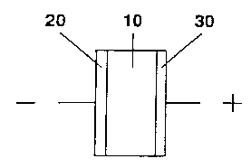
Fig. 1 is a simplified front view illustration of an x-
ray or gamma ray detector constructed and operative in accordance
with one preferred Qmbodiment of the present invention;
Fig. 2 is a simplified front view illustration of an x-
ray or gamma ray detector constructed and operative in accordance
with another preferred embodiment of the present invention;
Fig. 3 is a simplified diagram of a preferred system
for measuring a photocurrent induced by x-rays or gamma rays; and
- Fig. 4 is a simplified block diagram of preferred
spectroscopy apparatus constructed and operative in accordance
with a preferred embodiment of the present invention;
Fig. 5 is a front view illustration of a detector which
is a variation of the detectors of Fig. 1 or Fig. 2 in that the
positive contact is surrounded by a guard ring contact; and
Fig. 6 is a side vlew illustration of the detector of
Fig. 5.
SU5STITUTE SHEET (RULE 26)
~ ._
WO96105521 2 1 97 1 96
DETAILED DESCRIPTION OF PREFERRED EMBOOIMENTS
Reference is now made to Figs. 1 and 2 which are
simplified illustratiDns of an x-ray or gamma ray detector
constructed and operative in accordance with two respective
alternative embodiments of the present invention.
The x-ray or gamma ray detectors of Figs. 1 and 2 may
be constructed by the following method:
a. Provide a CdTe crystal 10, preferably a high-resistance
indium-doped n-type CdTe crystal which may be manufactured in
accordance with conventional methods such as that describe~ in K.
Zanio et al, IEEE Trans. Nucl. Sci., NS21, 31~, 1974
b. Attach contacts to the CdTe crystal, using conventional
methods such as the method described in R. E. Braithwaite et al,
sOlid State Electron., 23, 1091, 1980. According to one preferred
embodiment of the present invention, as ill~strated in Fig. 1,
the contacts comprise a negatively biased contact Z0 which pro-
vides free entrance of electrons into the crystal, anC a posi-
tively biased contact 30 which provides free exit of electrons
from the crystal. The contacts 20 and 30 may, for example, be
formed by deposition of indium on the crystal 10.
According to an alternative embodiment of the present
invention, the CdTe crystal 10 may comprise a high-resistance
chlorine-doped p-type CdTe crystal which is manufactured in
accordance with conventional methods such as that described in B.
Biglari et al, Phys. Stat. Sol . (a)100, pp. 589-~96, 1987. In
this embodiment, the positively biased contact 30 provides free
entrance of holes Lnto the crystal and the negatively biased
contact 20 provides free exit of holes from the crystal. The
16
SUEiSTlTUTE SHEET (RULE 26)
2 1 971 96
WO96105521 I~l/u~ S
contacts 20 and 30 may, in this embodiment, be formed by
deposition of a thin layer of conductive p-type CdTe on the
crystal 10.
An alternative to the detector of Fig 1 is illustrat-
ed in Fig. 2, in which the negatively biased contact 20 provides
free entrance of electrons into a high resistance n-type CdTe
crystal 10 and a positively biasèd contact 40 provides free
entrance of holes into the crystal. The negatively biased contact
may, for example, be formed by deposition of indium on the
crystal 10. The positively biased contact 40 may, for example, be
formed of a thin layer of conductive p-type CdTe deposited on the
crystal 10.
According to an alternative implementation of Fig. 2,
the positively biased contact 40 provides free entrance of holes
into the high resistance p type crystal and the negatively biased
contact 20 provides free entrance of electrons into a p-type
crystal. The positively biased contact 40 may, for example, be
formed by deposition of a thin layer of conductive p-type CdTe on
the crystal 10. The negatively biased contact 20 may, for
example, be formed of indium deposited on the crystal.
Reference is no~ made to Fig. 3 which is a simplified
diagram of a preferred system for measuring a photu~uLL~nL in-
duced by x-rays or gamma rays. The system of Fig. 3 preferably
includes a detector 44 ~hich may be based on the detectors of
Figs. 1 and 2, connected to a voltage bias source ~0 such as a
battery or power supply, an electrical current measurement device
such as an ammeter and a radiation source ~0 which may com-
SUE~STITUTE SHEET (RULE 26)
WO96/05~21 2 1 9 7 t ~ 6 ~ 5~ ~
prise an x-ray tube which irradiates an object to be inspected,
or alternatively a gamma source such as a gamma radioactive
material.
Preferably, the mode of operation of the system of Fig.
3 is as follows:
a. The CdTe crystal is irradiated by a flux of x-ray
photons or gamma ray photons.
b. As each photon is absorbed by the CdTe crystal, it
generates equal numbers of electrons and holes. These electrons
and holes flow in opposite directions, under the influence of the
bias voltage applied to the detector contacts 20 and 30. The
electrons flow toward the positive contact whereas the holes flow
toward the negative contact.
In the detector of Fig. l, if the crystal is an n-type
crystal, an electron reaching the positive contact leaves the
crystal by entering the contact. In the detector of Fig. 2, an
electron reaching the positive contact disappears by recombina-
tion with a hole injected into the crystal by the positive con-
tact.
If the crystal is a p-type crystal, then, in the
detector of Fig. l, a hole reaching the negative contact ~leaves
the crystal by entering the contact. In the detector of Fig. 2, a
hole reaching the negative contact disappears by recombination
with an electron injected into the crystal by the negative con-
tact.
c. This flow of electrons and holes results in an electric
current measured by the ammeter 60. According to the general
theory of photoconductivity, this current continues, as more
~ WO9~05521 2 1 ~ 7 1 9 6 P~ "6~
electrons or holes are free to enter the crystal through the
negative or positive contact, respectively, and leave it through
the positive or negative contact, respectively, until electrons
and holes disappear in pairs within the crystal by electron hole
recombination.
The electron or hole transition time through the crys-
tal is inversely proportional to the bias voltage. Therefore,
application of a sufficiently high bias voltage causes the tran-
sition time to become shorter than the electron or hole recombi-
nation time. The photocurrent includes both electrons and holes
originally generated by the photons, and electrons or holes
entering the crystal through the contacts. Whenever the transi-
tion time is shorter than the recombination time, the photocur-
rent is significantly amplified (current gain) compared to the
current due only to the electrons and holes originally generated
by the photons.
For example, for a detector having a l.5 mm distance
between the contacts, and a bias voltage of 20~0 V, amplification
by a factor of 2~C may be obtained, relative to the signal
obtained with a conventional detector which is similar in every
respect except that the contacts are blocking.
As described above, the contacts allow free charge flow
into and out of the crystal so that the dark curren~ in the
detector shown and described herein is high compared to conven-
tional CdTe detectors eouipped with blocking contacts. ~owever,
since the current gain is also high in the detector shown and
described herein, relative to a conventional detector, the
19
SUBSTITUTE SHEET (RULE 26)
,
W096/0552~ 2 1 ~ 7 1 9 6 F~ ;;J9~ -
signal-to-dark current ratio is comparable to or better than that
of a conventional detector.
A further advantage of the system of Fig. 3 is that the
current is not affected by hole trapping within the crystal, in
contrast to conventional detectors_
Reference is now made to Fig. 4 which is a simplified
block diagram of preferred spectroscopy system constructed and
operative in accordance with a preferred embodiment of the
present invention in which the charge generated by individual x-
ray photons or gamma ray photon-s is measured.
The system of Eig. 4 pre~erably includes the following
components:
a. A source 70 of x-ray or gamma rays. For example, the
source may comprise an x-ray source such as an x-ray tube which
irradiates an object to be inspected. Alternatively, the source
may comprise an object to be inspected which incorporates within
it a radioactive source, such as a patient to whom a drug con-
taining a radioactive source has been administered.
b. An x-ray or gamma ray detector 74 which may be based or,
the detectors of Figs. 1 or 2;
c. A voltage bias source 50 such as a battery or a power
supply:
d. A preamplifier 80 such as an EG&G ORTEC model =number
142A;
e. A spectroscopy amplifier 90, such as an EG&G ORTEC
model number 572;
f. A multi-channel analyzer (MCA) 100 such as an EG&G
ORTEC model number 916; and
gJBSTITUTE SHEET ~Bi~.E ~j
2 t 97 ~ 96
~ WO 961055~ J,,75/G~965
g. A computer llO such as an IBM AT 286.
Units 80, 90, 100 and 110 are commercially available as
a single module, namely the Gamma Spectroscopy System, marketed
by EG&G ORTEC_ ~
Preferably, the mode of operation of the system of Flg.
4 is as follows:
a. The CdTe detector is Lrradiated by a flux of x-ray
photons or gamma ray photons.
b. As a single photon is absorbed by the CdTe crystal, it
generates equal numbers of electrons and holes. These electrons
and holes flow in opposite directions, under the influence of the
bias voltage applied to the detector contacts 20 and 30. The
electrons flow toward the positive contact whereas the holes flow
toward the negative contact.
If the crystal is an n-type crystal, then, in the
detectcr of Fig. 1, an electron reaching the positive contact
leaves the crystal by entering the contact. In the detector of
Fig. 2, an electron reaching the positive contact disappears by
recombination with a hole injected into the crystal by the posi-
tive contact.
Simultaneously with the above-described electron and
hole flow, other electrons enter the crystal from the negative
contact and flow toward the holes.
The flow terminates when all the electrons and holes
- disappear from the crystal either by exiting through the
contacts, or by electron hole recombination within the crystal.
The spectroscopy system of Fig. 4 measures the charge
21
SUBSTIT~ITE SHEET (~ULE 2~)
2 ~ 97 ~ 96 ~
WO96/05521 ~ 55
collected from each single photon absorbed by the detector, and
provides the statistical distribution of charges of all the
photons absorbed by the detector.
In the present invention, holes recombine with
electrons arriving from the negative contact. In contrast, in
conventional CdTe detectors, holes mu5t flow all the way toward
the negative contact. Since electron flow is faster than hole
flow, the time required for complete charge collection in the
detector of Figs. l or 2 is shorter than in conventional CdTe
detectors.
~ ue to the shorter charge collection time provided by
the method of the present invention, spectroscopic measurements
may be carried out by the system of Fig. 4 with a higher signal-
to-noise ratio and/or at higher photon flux rates, compared to
conventional CdTe detectors.
A further advantage of the system of Fig. 4 is that the
detector is not adversely affected by hole trapping within the
crystal.
Suitable materials for use in the spectroscopy system
of Fig. 4 include the following high resistance n-type crystals:
a. cadmium telluride;
b. Alloys thereof in which an additional material such as
zinc replaces a certain percentage of the cadmium (Cdl_xZnxTe
where 0 <=x <= l).
c. Alloys thereof in which an additional material such as
selenium replaces a certain percentage of the tellurium
(CdTel_xSex where 0 ~-x <~
d. Combinations of a, b and c.
SUBSTITUTE SHEET (RULE 26)
-
21 q7 1 q6
1 I/IJ JJ~
WO 96105511
The n-type crystal may be doped with materials such
as: indium, gallium, aluminum, chlorine, bromine or iodine.
Contacts providing frea flow of electrons to and from
the crystals, for use in the spectroscopy system of Fig. 4 may be
formed of indium, cadmium, aluminum, gallium, and alloys includ-
ing these materials. Also, any n-type conductive semiconductor
may be employed such as n-type conductiye CdTe, n-type conductive
CdS, n-type conductive ZnSe, and n-type conductive HgxCdl_xTe (0
=< x =< 1).
Contacts providing free flow of holes to the crystals,
for use in the spectroscopy system of Fig. 4 may, for example, be
formed of gold~ piatinum, copper, osmium, nickel, tellurium,
antimony, carbon, and alloys including these materials, as well
as p-type conductive semiconductors such as p-type conductive
CdTe or p-type conductive HgxCdl_xTe (0 =< x =< 1). or p-type
conductive HgTe.
A preferred method for producing p-type HgTe is de-
scribed in E. Janik and R. Triboulet, "Ohmic contacts to p-type
cadmium telluride and cadmium mercury telluride", J. Phys. D.:
Appl. Phys., 16 (1933), 2333 - 2340.
~ uitable crystals for use in the photocurrent measure-
ment system of Fig. 3 include the crystals described above as
suitable for the embodiment of Fig. 4 and, additionally, similar
crystals which are high-resistant p-type instead of n-type.
The p-type crystal may be doped with materials such as:
chlorine, bromine, iodine, copper, chromium or vanadium.
Contacts providing free flow of electrons to p-type
SUBSTITUTE SHEET (RULE 26)
21 ~71 ~6
WO96105~21
crystals, for use in the photocurrent measurement system of Fig.
3 may be the same as the contacts, described above with refer-
ence to Fig. 4, which provide free flow of electrons to and from
n-type crystals.
Contacts providing free flow of holes to and from p-
type crystals, for use in the photocurrent measurement system of
Fig. 3 may, for example, be the same as the contacts, described
above with reference to Fig. 4, which provide free flow of holes
into n-type crystals.
The operation of detectors made of p-type crystals is
generally the same as the operation of detectors having n-type
crystals, as described above with reference to Fig. 3, except
that the major electric current carriers are holes rather than
electrons.
According to a prefer~red embodiment of the present
invention, as illustrated in Figs. 5 and 6, a guard ring 120 is
provided which ~uLLuu--ds at least one of the contacts, such as
the positive contact 30 (Fig. 1) or 40 (Fig. 2). The guard ring
reduces deterioration of the detector's performance due to the
influence of the detector's side walls 130 The guard ring may be
identical in configuration and as to material to the positive
contact 30. The embodiment of Figs. 5 and 6 is suitable for the
spectroscopy application of Fig. 4.
One preferred method for fabricating the positive
contact and the guard ring is as follows:
a. Fabricate the positive contact;
b. Using photolithographic techniques, separating a guard
ring out of the positive contact.
24
SU~ST~TUTE SHEET (~ULE 26)
~ W096105521 ~1 9 7 1 ~ 6 r~ t . -
In the present speci~ication and claims, the term
''cadmium telluridel' or IlCdTell is used to refer either to
undopedCdTe or, preferably, to doped CdTe.
It is appreciated that various features of the
invention which are, for clarity, described in the contexts of
separate embodiments may also be provided in combination in a
single embodiment. Conversely, various features of the invention
which are, for brevity, described in the context of a single
embodiment may also be provided separately or in any suitable
subcombination.
It will be appreciated by persons s~illed in the art
that the present invention is not limited to what has been
particularly shown and described hereinabove. Rather, the scope
of the present invention is defined only by the claims that
follow:
SUBSTITUTE SHEET(RULE 2~)