Note : Les descriptions sont présentées dans la langue officielle dans laquelle elles ont été soumises.
'_ 2 1 9738 1
TITLE:
Power Resistor
FIELD OF THE INVENTION:
The present invention relates to electrical resistors,
and more particularly to electrical resistors used in high
power applications.
BACKGROUND OF THE INVENTION:
High power electrical resistors are known and used in
many applications. For example, power resistors are used by
heavy industry and electrical utilities as neutral grounding
resistors; damping resistors; in harmonic filters; in speed
controls; for motor starting; and the like.
Known power resistors may take the form of an edgewound
conductor mounted on a insulating core. For example one
such resistor is formed by winding a steel strip about the
edge of a ceramic core. Alternatively, insulated wire
conductor mounted about an insulating core forms a wire
wrapped resistor.
Other power resistors take the form of a solid
conductive ribbon, having a current path from end to end.
The ribbon is bent in an accordion-like shape to reduce the
size of the resistor while maintaining the relatively long
- 1 --
91634-7 MZ/br/tm
2 1 9738 1
current conducting path. Further known resistors are made
-of a plurality of stamped grids connected in series, or of a
helical wire wrapped about a cylindrical core.
As is well known and understood, the resistance of a
resistor is directly proportional to the effective length of
the conductive element used to form the resistor. The
resistance of the known power resistors is thus limited by
the length of conductive material used to form the resistor.
One further known design incorporates a resistive slab
having a plurality of circular holes or slots. These
circular holes create a non-linear current path along the
resistor, and provide for improved heat transfer and
ventilation of the resistor. However, the choice of
arrangements of circular holes does not provide for an
optimum resistance.
It is an object of the present invention to provide an
improved power resistor that overcomes some of the
disadvantages of known devices.
SUMMARY OF THE INVENTION:
In accordance with one aspect of the present invention,
there is provided, a power resistor comprising a first
electrical connection terminal and a second electrical
connection terminal; a resistive element extending between
- 2 --
91634-7 MZ/br/tm
'- 2! ~7381
said first terminal and said second terminal said element
having, a plurality of first insulating regions, extending
generally parallel to each other along said element arranged
in a first row along said element; each of said insulating
regions having a first orientation in said row, and each of
said regions having a first shape, said shape being
asymmetric about an axis transverse to said first row; a
plurality of second insulating regions, having generally
said first shape and an orientation substantially opposite
said first orientation; said second regions extending
generally parallel to each other arranged in a second row,
said second row arranged generally parallel to said first
row along said element, each said second insulating region
extending between two of said first insulating regions;
whereby said first and second insulating regions define a
tortuous current path from said first terminal to said
second terminal.
In accordance with another aspect of the present
invention, there is provided a power resistor comprising a
first electrical connection terminal and a second electrical
connection terminal; a resistive element extending between
said first terminal and said second terminal, said resistive
element having a plurality of first insulating regions, each
first insulating region having a central portion with two
wings, one wing extending from either side of said central
region such that a tip of each wing is more proximate said
first terminal, in a direction extending along said element,
than is said central portion; a plurality of second
-- 3
91634-7 MZ/br/tm
- ' 21 97381
insulating regions, each second insulating region having a
central portion with two wings, one wing extending from
either side of said central region such that a tip of each
wing is more proximate said second terminal, in a direction
extending along said element than is said central portion;
for each first insulating region, one wing of each of two
second insulating regions extends between the wings of the
first insulating region, whereby said first and second
insulating regions define tortuous current paths from said
first terminal to said second terminal.
BRIEF DESCRIPTION OF THE DRAWINGS:
In drawings which illustrate embodiments of the
invention,
Figure 1 is a resistive slab forming part of a power
resistor in accordance with one aspect of the present
invention;
Figure la is an enlarged view of a portion of Figure l;
Figure lb is a cross-sectional plan view of Figure la,
along lb-lb;
Figure lc is a side plan view of a portion of Figure l;
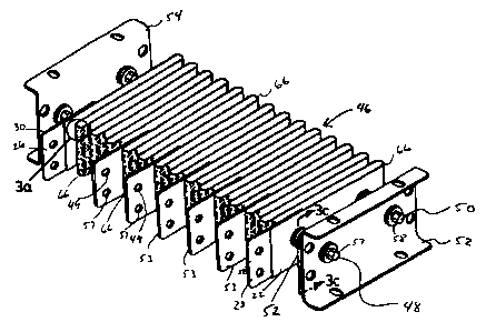
Figure 2 is a ribbon resistor in accordance with
another aspect of the present invention;
-- 4
91634-7 MZ/br/tm
'- 21 97381
Figure 2a is an enlarged view of a portion of Figure 2;
Figure 2b is a top plan view of Figure 2a;
Figure 2c is a cross-sectional view of Figure 2a, taken
along 2c-2c;
Figure 3 is a~bank of power resistors in accordance
with an aspect of the present invention;
Figure 4 is a resistive slab in accordance with a
further aspect of the invention;
Figure 4a is an enlarged view of insulating regions in
accordance with a further aspect of the invention;
Figure 5 is an enlarged view of insulating regions in
accordance with a further aspect of the invention;
Figure 6 is an enlarged view of insulating regions in
accordance with a further aspect of the invention;
Figure 7 is an enlarged view of insulating regions in
accordance with a further aspect of the invention;
25 .
DETAILED DESCRIPTION OF THE PREFERRED EMBODIMENTS:
With reference to Figure 1, a power resistor 20
comprises a resistive element in the nature of resistive
-- 5
91634-7 MZ/br/tm
21 97381
slab 22 having a plurality of insulating regions 24.
Resistive slab 22 is made of a conducting material such as
steel (grey painted, mill galvanized or stainless, for
example), aluminum or other metal; carbon; or a suitable
alloy. The slab has a length (1) and generally uniform
width (w) and thickness (t). Terminal connection points 26
and 28 are located proximate ends 30 and 32 of slab 22.
As best illustrated in Figure la, each insulating
region 24 preferably has a generally chevron shape. Each
chevron shape comprises a central portion 34 with two wings
36 and 38. Insulating regions 24 are formed by cutting or
stamping out portions of the conductive material forming
slab 22. Thus, insulating regions 24 are actually air gaps
in slab 22. The stamping allows for the inexpensive
production of the power resistor 20, from a resistive slab
22 made of a single material.
Insulating regions 24 are arranged in generally
parallel rows extending from proximate one end 30 of slab 22
to the other end 32. Each row comprises a plurality of
chevron shaped regions having a generally parallel
orientation, with wings 36 and 38 of each chevron in a row
either extending from central portion 34 toward end 30 or
extending from central portion 34 toward end 32. The
central portions 34 of all chevron shaped regions in a row
are generally aligned along an axis parallel to the sides
40, 42 of slab 22. Adjacent rows of chevron shaped regions
are also generally parallel. The chevrons of adjacent rows
-- 6
91634-7 MZ/br/tm
21 97381
have opposite orientations and are interleaved so that each
wing of each chevrons in one row extends between two wings
of chevrons in a neighbouring row (Figure la).
Additionally, a row of partial chevrons extends along each
side 40 and 42 of slab 22, thereby making sides 40 and 42
jagged, and interrupting any direct current path from
terminal 26 to terminal 28 along and proximate sides 40, 42.
End 30 of slab 22 is suitable for electrically
connecting slab 22 to an identical slab 22 at its opposite,
complementary end 32. End 30 is kinked slightly as
illustrated in figure lc, in order to receive a
complementary end the further identical slab generally flush
with the surface of of slab 22.
Slab 22 further comprises mounting holes 44, along its
centre between sides 40 and 42 of slab 24 and at regular
intervals along its length.
As illustrated in Figure 2, a plurality of slabs 22 may
be interconnected at their ends (ie. end 30 of one slab to
end 32 of another) and may be folded at regular intervals to
form an accordion-like ribbon resistor assembly 46. The
folded slabs 22 are mounted on rods 48 and 50, with each
mounting hole 44 (Figure 1) engaging a rod 48 or 50. Every
other mounting hole (Figure 1) engages one rod 48, while the
remaining mounting holes engage a second rod 50. This
folded arrangement allows slabs 22 almost thirty feet in
length to be folded into a ribbon resistor assembly 46
-- 7
91634-7 MZ/br/tm
21 97381
slightly longer than two feet. Of course, if a single slab
of thirty feet can be manufactured assuring for proper
alignment of insulating regions 24, several slabs do not
need to be attached end to end.
As shown in Figure 2c, rod 48 has a circular cross-
section and is made of a rigid conducting material. Two
spacer washers 51 and an insulating washer 53 are used to
keep each folded portion of slab 22 at a fixed distance from
each adjacent folded portion. Spacer washers 51 are made of
a conductive material, such as galvanized steel, but are
spaced by thin insulating washer 53. Insulating washer 53
may be made of mica and prevents electrical contact between
adjacent folded portions of slab 22. Proximate an end of
rod 48, washers 80, 81, 82, 83 and 84; mica spacers 86 and
87; and nut 89; all space slab 22 from end plate 52. With
reference to Figures 2 and 2c, rods 48 and 50 are threaded
at their ends and bolted to end plates 52, 54 which act as
mounts. Moreover, end plate 52 is attached to rod 48 by
mica spacer 88; washer 85; and nut 57 (Figure 2c). An
identical arrangement is provided at each end of rod 48, and
for rod 50.
Heavy terminal plates 53 (Figure 2) are mechanically
clamped and welded to slab 22 and feature a two hole 49, 57
industry standard NEMA bolt pattern. Terminal plates 53 act
as electrical connection points to resistor element 46.
Resistor assembly 46 may be formed in standard "Mill Bank"
-- 8
91634-7 MZ/br/tm
2 1 9738 1
dimensions to insure interchangeability with existing power
resistors.
As illustrated in Figure 3, a slab similar to slab 22
may also be rolled lengthwise to form a generally
cylindrical resistive element 56. A plurality of
cylindrical resistive elements 56 may be mounted on two end
plates 58 and 60 to form a tubular resistor bank 62. End
plates 58 and 60 are also formed of an insulating material.
For the purpose of mounting cylindrical resistor elements
56, pins or bolts extending radially through the cylindrical
resistor elements 56 keep the elements 56 mounted to end
plates 58 and 60. These pins or bolts (not shown) may
extend radially through cylindrical elements 56 on one or
both sides of end plates 58 and 60. Similarly, end plates
58 and 60 have appropriate sized holes 64 for mounting a
plurality of cylinders 56. The mounting holes 64, however,
do not electrically connect cylindrical resistive elements
56 to end plates 58 and 60. Of course, these individual
cylindrical resistive elements 56 may be connected in
parallel or series depending on the required application.
Electrical connection to the resistor bank 62 may be
effected at terminals at the ends of cylindrical resistors
56 near end plates 58 and 60.
When an electric potential is applied to the terminals
of resistor 20 of Figure 1, resistor assembly 46 of Figure 2
or resistor bank 62, Figure 3, a current inversely
proportional to the resistance of the resistive element
g
91634-7 MZ/br/tm
2197381
between the terminals will flow between the terminals.
Typically AC voltages from 120 V to 2 kV are applied.
Without insulating regions 24, the resistance of slab
22, for example, between its ends from which each resistive
element is formed could easily be calculated as
R=pxlength of slab/(cross-sectional area of slab)
wherein p= resistivity per unit length of the
conductive material used to form slab 22.
With the addition of insulating regions 24, however,
current can no longer flow directly from one end of the slab
22 to the other. The arrangement of insulating regions 24
on the slab 22 creates a tortuous current path between
terminals 26 and 28. Thus, instead of flowing directly from
one end to the other, current must flow between regions 24
in a generally zig-zag path which, for resistor 20, is
illustrated in Figure la. Thus, the length of the effective
current path between terminals 26 and 28 is significantly
greater than length (l) of the slab 22, as the current will
traverse the insulating regions. As the length of the
current path is increased, so is the effective resistance of
the slab between terminals 26 and 28.
As illustrated in Figure lb, the cross-sectional area
along the tortuous path is reduced from that of the entire
slab to the cross-section of the portions between resistive
- 10 -
91634-7 MZ/br/tm
' 21 ~738 ~
regions 24, thus further increasing the resistance along
this path.
Empirical evidence indicates that the resistance of
resistive slab 22 is between ten and twenty times as great
as the resistance of a known ribbon resistors. Known ribbon
resistors have a resistance of approximately 0.05 ohms,
while resistors of similar dimensions, as disclosed herein,
have resistance measured at approximately 0.72 ohms.
Additionally, as will be appreciated, in typical
applications a power resistor 20 must dissipate several
kilowatts of electrical power, as heat. Thus, the
temperature of the resistive element(s) may reach several
hundred degrees celsius. As resistive regions 24 are air
gaps, they facilitate heat transfer from the resistive
element to the environment. Moreover, experiments shows
that in the embodiment of Figure 3 regions 66 near bends
along the resistive element reach the highest temperatures.
As shown in enlargement in Figures 3a and 3b, the chevron
shaped insulating regions 24 coincidentally stretch and fan
outwardly near these bends, thus providing for further
improved heat transfer and cooling near bend regions 66.
As illustrated in Figure la, the edges of insulating
regions are preferably smoothed or rounded. This smoothing
reduces the existence of eddy currents at or near cusps
along the current paths which may be induced by AC currents
flowing along the tortuous path along slab 22.
- 11 -
91634-7 MZ/br/tm
2 1 9738 1
It will be appreciated that insulating regions 24 do
not need to be chevron shaped nor have rounded edges, but
may take other forms to create a tortuous path between
connection points on the resistive element 22, so that the
current along the path does not flow in one direction from
one connection point to the other on the resistive element,
in accordance with the invention.
For example, Figures 4, 4a and 5 depict embodiments of
the invention in which insulating regions are formed by
chevron shaped cut-outs (68, 70) having minimally rounded
edges (68 in Figure 4a) or having straight edges and corners
(70 in Figure 5). Both these embodiments, employ the
present invention but may not reduce the eddy currents as
well as the embodiments of Figures 1-3.
Similarly, as depicted in Figures 4, 6, and 7, the
present invention does not require chevron shaped insulating
regions. Instead, many different configurations having
insulating regions arranged in generally parallel rows, each
with wings and wings of adjacent rows arranged in an
interleaved relationship will create a tortuous path as
required.
For example, Figures 4a and 6 show another preferred
embodiment of the invention, in which the insulating regions
72 comprise generally U-shaped cut-outs along slab 74. Each
U shaped cut-out comprises a central portion 76 with two
wings 78 and 79. U-shaped regions in one row are arranged
- 12 -
91634-7 MZ/br/tm
21 97381
convexly away from an end of the resistive element, while U-
shaped regions in an adjacent row are arranged convexly
toward that same end. These insulating regions 72 are
arranged so that wings 78, 79 of one row of U-shaped cut-
outs are interleaved between the wings 78, 79 of an adjacent
row of U-shaped cut-outs thus defining a tortuous current
path along the slab, as shown.
Figures 4a and 7 illustrate a further embodiment of the
invention. Insulating regions 90, comprise generally semi-
circular arcs. The semi-circular arcs are arranged in rows
along the length of the slab, with adjacent rows of arcs
having opposite orientation. Arcs in one row are arranged
convexly away from an end of the resistive element, while
arcs in an adjacent row are arranged convexly toward that
same end. The arcs in adjacent rows are further interleaved
so that each wing or tip of one arc rests between the wings
or tips of an arc of an adjacent row of cut-outs.
Moreover, a person skilled in the art will readily
realize that other modifications to the preferred
embodiments are possible. For example, the insulating
regions need not be air gaps but may be formed of other
insulators such as glass or ceramics. The connection points
to the resistor need not be at opposite ends of the
resistor, but may be at points along the sides of resistive
elements, as illustrated in Figure 2.
- 13 -
91634-7 MZ/br/tm
'- 2 1 9738 1
A person skilled in the art will understand that the
invention is not limited to the illustrations described and
shown herein, which are deemed to be merely illustrative of
the best modes of carrying out the invention, and which are
susceptible to modification of form, arrangement of parts
and details of operation. The invention, rather, is
intended to encompass all such modifications which are
within its spirit and scope as defined by the claims.
- 14 -
91634-7 MZ/br/tm