Note : Les descriptions sont présentées dans la langue officielle dans laquelle elles ont été soumises.
Wo 96/07939 2 i ~ 9 3 3 8 PcrlAus5/oo542
DIFFRACTION SURFACES AND METHODS FOR THE
MANUFACTURE THEREOF
Technical Field
The present invention relates to the production of projected images from an optically
5 diffractive surface. These images may be confirrnPd either visually or by m~rhin~ in
order to ~ h~ irate the optical surface or for other purposes such as data storage or
entert~inmlont
Background of the Invention
A current problem is the sale of cou~ reiL goods. C~ullL~lrri~hlg is often inhibited
o by the use of labels and tra~1P~ . However unauthorised use of the labels and
tr~dem~rkc is (~ r~lt to prevent.
The above problems are ~ cllcsed in Ill~ ional Application PCT/AU92/00252.
Object of the Invention
It is the object of the present invention to overcome or substantially ameliorate the
15 above problems.
Summary of the Invention
There is disclosed herein A method of producing a diffraction pattern including a
diffraction grating, the pattern when illl~.--i..~lrd producing a recognisable image on a
surface inl~lcepLing dirr,ac~d light resulting from the illulllh~lion, said method including
20 the steps of:
providing a ~lilllaly data stream h,dicdLive of the image;
processillg the primary data to ~t~ ...;..~ the configuration of said grating and
thelerole said pattern, with a characteristic of the processed primary data coll~s~,onding
to a physical ch~c~ ic of the grating;
providing a plate having a surface to be defolllRd to have a configuration
corresponding to said pattern;
defolllling the plate surface in accordance with the processed primary data so as to
produce said configuration; and wherein
a physical dimension of the grating is deL~ led by said characteristic.
Brief Description of the Drawings
A preferred form of the present invention will now be described by way of example
with lefe~ence to the accolllpallying drawings wherein:
Figure 1 is a schPm~tic illustration of an image and a process for producing a
diffraction grating from an ima~e;
Figure 2 is a schematic illustration of data from which a diffraction grating may be
produced;
SUBSTITUTE SHEET (RULE 26)
wo 96/07939 -2- ~ 1 9 9 ~) 3 ~ PCr/AUg5l00542
Figure 3 is a sc~ ;r l~rcsc~ lion of a dirLa~;lion grating;
Figure 4 is a srh~m~tir illustration of an optical surface comprising a first region, a
second region and a so-called transition region;
Figure 5 is a sch~m~tir illustration of a close-up view of the optical surface of
Figure 4 showing the surface to be made up of cells;
Figure 6 is a sch~ lir illustration of the optical prol,e,Lies of the first and second
regions of Figure 4;
Figure 7 is a sch~m~tir illustration of a portion of a cell of the optical surface of
Figure 4 showing the cell to be made up of so-called blocks;
Figure 8 is a srh~m~tir illustration of a single block of Figure 7;
Figure 9 is a srh~m~tir illustration of an optical surface of a type which produces
projected images from an incident light beam;
Figure 10 is a sch~ lir illustration of an example of a movement animation effect
in the projected images of Figure 9;
Figure 11 is a schPm~tir illustration of an example of an h~Lensily animation effect
in the projected images of Figure 9; and
Figure 12 is a sch~ ir illustration of a close-up view of a prefe,.~d embodimentof a design for the optical surface illustrated in Figure 9.
Detailed Descr;~liGI~ of the Plafe..ad EmbG~ .a,.l
In Figure l(a) there is illustrated an image from which a dirrlacLion grating will be
produced so that if the grating is illu~ ul~d by a suitable light source the diffracted light
will produce the image on a screen. A solid state laser is an example of a suitable ligh~
source. More particularly, the actual grating itself cannot be conveniently directly viewed
for the l~u-~ose of seeing the image. The dirrlacled image can only be seen via
25 a~ (Opliàte i~ in~lion of the grating in which case the image will be seen on a screen
ceivillg the diffracted light from the grating.
It should be noted that the image of Figure l(a) includes shaded (i.e. grey scale)
regions. To Illdllurh-;lule the diffraction grating the image of Figure l(a)j or a rearranged
version of it, as described below, is sc~nn~d so as to produce a stream of data indicative
30 of the image. The stream of data is obtained by dividin~ the irnage into a number of
pixels or elements, and determinin~ a data value or set of data values indicative of each
pixel or element. The density of pixels in the sc~nning process is chosen so as to produce
the required image quality in the diffracted images. For example, the ima_e may be
sc~nn~od into a 128 by 128, or 256 by 128, or 512 by 256 array of pixels. The two
35 dimensional fast Fourier Transform can then be used to compute from the stream of data
the diffraction irna~e from which the diffraction grating is produced. In general the fast
Fourier Transform of an albiLld.y image consists of two non-zero parts: a so-called real
part and a so-called im~gin~ry part.
SUBSTITUTE SHEET tRULE 26)
Wo 96/07939 2 1 9 ~ 0 3 8 Pcr/Aus5/00542
-
-3-
In the present invention the original input image (for example, the image of figure
l(a)) is processed so that the Fourier Lldl~ru,lll of the reslllting processed image has
negligible im~gin~ry component - i.e. so that the Fourier Ll~ro~ is real-only.
Preferred m~thl tlc for geneldling the processed image are described below. The
5 diffracted image geneldted by the reslllting diffraction surface and projecled onto an
illklcepLillg screen then consists of the original image (such as the image of figure l(a))
plus a rotated version of the original image, with such an image pair (original image plus
rotated image) occurring about the speclll~r reflection (zeroth order diffracted beam) from
said diffraction surface and also less strongly about the higher diffraction orders from said
10 diffraction surface.
A ~liffirlllty with the Fourier Tl~r~rolll. technique as used conventionally is that
most of the hlrolllldlion in the Fourier Tldl~r,llll is contained in a small portion of the
Fourier Tlal~rollll data. In the present invention this means that only a small area of the
resulting diffraction pattern will be l~l,onsible for prodllcing the irnage. Concequently
15 much of the incident reading light beam will be diffracted into a conventional diffraction
spot, resulting in relatively little light hll~ily in the diffracted images. A method of
ov~lcolll-ng this disadvantage is to mo~ te the data produced by the Fourier Tral~r(Jllll
through the use of a random phase noise array as described below. In the presentinvention the random phase noise array must preferably be odd S~llllll.LliC in two
20 dimPncions as described below.
A further hlll)ro~ lclll to the dirrldckd images can be made through clipping and
in~ of the data provided by the fast Fourier Tldl~rollll. The fast Fourier
Tldl~rullll data may be clipped to a yelc~llldge7 for example 50%, of the peak c~lcnl~tPd
level. The r~sllltin~ clipped data may then be qn~nti.ced into a discrete number of levels
25 within the clipping range. For example, the data produced by the fast Fourier Tld~ro
after clipping could be qu~nticed into fifly, or ten discrete levels within this clipping
range.
An example of a specific sequenre of functions, inrl~-ling variations, which may be
carried out in order to convert an original image into processed Fourier Transform data
30 from which the diffraction surface can be produced is as follows. This procedure is
illustrated in the sequenre of illustrations of figure 1.
It should be noted that the layouts referred to in the present description are those
which would be g~ dted and observed on a computer screen using a computer graphics
package such as Adobe Photoshop (or a similar package). It should also be appreciated
35 that the Cartesian coordinate system, and hence the X and Y axes, used in the following
descriptions are arbilldly and are included or referred to only for reasons of clarity of
explanation.
1. The original or input image is positioned in a rectangular input image area and
said re~ ëular input ima_e area is positioned in the upper half plane (positive Y values)
SUBSTITUTE SHEET (RULE 26)
Wo 96/07939 2 1 9 9 0 3 8 PCr/AU9S/00542
of a Cartesian coordinate system with the lower edge of said image area on the X axis of
said Cartesian coo~ ldte system, and the Y axis of said Cartesian cooldi"dte system
dividing said image area into two equal halves, as illustrated in figure l(a). The blac~;
area in figure 1(a) is the input image area which includes the input image - in this case the
5 image of an aircraft. It should be appreciated that the smaller the input image as a
opGlLion of said input image area the brighter (i.e. higher illl~nsiLy) the resnltin~
diffracted image. This can be understood in terms of the diffracted optical power from the
fini~h~d optical surface being an approximately fixed proportion of the inrirlent optical
power, so that making the diffracted images a smaller proportion of the total image plane
lO area conc~l,lldtes this approximately fixed l),o~o,lion of the incident power into a smaller
area, thereby inc,c,asing the diffracted image il,L~nsiLy.
2. The input image is ~ieiticerl The input image is divided into a Cartesian array
and each element, or pixel, in the array is acei~n~d a digitised, or qll~ntieerl, value according
to the values (e.g the grev scale level! of the co~ yollding pixel of the input image. The
15 array size is selected to provide the required resolution in the digitised image.
In the present pl~r~llcd embodiment of the processing technique a discrete fast Fourier
Transform is used to determine the diffraction grating data. The number of pixels in the X
and Y directions of the Cartesian tligitiein~ array should therefore preferably be a power of
2; for example the digitising array could be a 128 by 64 element array, or a 256 by 128
20 element array, etc.
The original image should preferably have black (i.e. zero valued) borders of at least
one pixel width all around, although this condition is not m~n~1~tory If non-zero pixels
occur on one or more borders, the im~ein~ry co"lpo~ of the resultant fast Fourier
Transform will tend away from zero, whereas ideally said im~in~ry co",pone,l~ should be
25 zero. However a small non-zero im~ein~ry cG"lponent in the fast Fourier Trdll~rollll output
may still result in a s~tiefActQry diffraction grating.
3. The 'quadrantised' image is produced from the digitised input image. There are
numerous variations on this quadr~ntieine process, all of which may produce satief~ctory
results for all practical purposes. Two such variations are described herein. The first
30 variation is a rigorously correct method which however leads to a minor defect in the image
generated by the resulting diffraction grating. while the second variation is anapproximation which removes the image defect resulting from the first variation.
Quadr~nticing Method: First Variation
(i) The original digitised image is mirrored into the bottom half plane (negative Y
3s values) of the Cartesian coordinate svstem, thereby producing an overall digitised image
twice the size of the original digitised input image, as illustrated in figure I (b).
(ii) The bottom half plane (negative Y values) image is mirrored about the Y axis
(i.e. Ieft to right and right to left)~ as illustrated in figure 1 (c).
SUBSTITUTE SHEET (RULE 26)
W096/07939 2 . 1 1 3 8 PcrlAu95loo542
(iii) The four Cartesian quadrants are diagonally ' ~wal~cd ' - i.e. diagonally
tr~n~l~t~d into the opposite quadrants. In other words, quadrant 1 is tr~n.~l~t~d into
quadrant 3, quadrant 3 is tr~n~l~ted into quadrant 1, quadrant 2 is tran~l~ted into quadrant
4 and quadrant 4 is transl~t~d into quadrant 2, thus producing the image of figure l(d)
5 from the image of figure l(c).
(iv) The left half plane (negative X values) of the resulting image is moved onepixel to the right (in the positive X direction), in the process discarding the right hand
column (at X = -1) of the left half plane and leaving a column of zero value pixels at the
left hand (m~rimllm negative X value) border. The bottom half plane (negative Y values)
10 iS moved one pixel down (in the negative Y direction), in the process discardillg the pixels
in the bottom (m~ximllm negative Y value) row and leaving a row of zero value pixels
immP~ t~ly bel.ow the Y axis (at Y = -1). Figure l(e) illustrates this method as applied
to the image of figure l(d). This method results in a 'black line defect' in the image
~e,~,aled from the rPcllltin~ dirrral-Lion surface, as described below.
Quadrantising Method: Second Variation
This method is an approximate method desi~n~d to remove the 'black line defect'
genel~led by the first variation above.
The second variation involves steps (i), (ii) and (iii) above of the first variation,
followed by the following step (iv).
(iv) The left half plane (negative X values) of the resulting image is moved onepixel to the right (in the positive X direction), in the process disca,~ing the right hand
column (at X = -1) of the left half plane and leaving a column of zero value pixels at the
left hand (m~ximllm negative X value) border. The right hand column (m~ximllm X
value) of the image is then copied into the zero filled left hand colurnn (m~ximllm
25 negative X value) of the image. The bottom half plane (negative Y values) is moved one
pixel down (in the l~e~aliv~ Y direction), in the process discal~ g the pixels in the bottom
(m~ximll~ ega~ive Y value) row and leaving a row of zero value pixels imm~ tely
below the Y axis (at Y = -1). Figure l(f) illustrates the ima~e obtained from this method
as applied to the image of figure l(d). This method results in a diffraction surface which
30 does not generate the abovementioned 'black line defect'.
4. The odd symmetric random phase noise contribution is determined. The
smaller 16 by 16 array of figure l(g) is used herein to illustrate the method for
de~ illg the random phase noise contribution. The X and Y Cartesian axes of figure
l(g) are included for ease and clarity of explanation, as in the other illustrations of figure
35 1. The method of construction of a random phase noise array, such as the 16 by 16 array
of fi~ure 1(g), is as follows.
(i) If the rligiti~ed input image is a 2P (in the X direction) by 2q (in the Y
direction) image, a 2P-1 by 2q array is first general~d and positioned into quadrant 1 of a
SUBSTITUTE SH EET (RULE 26)
- -
Wo 96/07939 PC rlAug5lo0542
2 1 ~ 9 0 38 -6-
Cartesian cooldh~dl~ system. The 2P-1 by 2q array is allocated a random number set, with
each pixel in the array being allocated a random number, except that the leR hand column
(at X = 1) and topmost row (~ ... Y value) are zero filled (i.e. have zero value).
The random ~ ber~ allocated to the pixels in the array are allowed to range between 0
and 359 and represent a random phase angle to be associated with the co"esponding
pixels of the ~igiti~ed and quadrantised input image.
(ii) The first quadrant random number array is mirrored about the Y axis into
quadrant 2 of the Cartesian coo~dindt~ system, and the mirrored quadrant 2 array shiRed
one pixel to the right (in the positive X direction), in the process discarding the zero filled
right hand column (at X = -1) and leaving a zero filled left hand (maximum negative X
value) column.
(iii) The resllltin~ top half plane (positive Y values) array is mirrored about the X
axis and the reslllting bottom half plane (negative Y values) array shiRed one pixel down
(in the negative Y direction), in the process discardillg t~e zçro filled bottom (m~Yimum.
negative Y value) row and leaving a zero filled row imm~Ai~tely below the X axis (i.e. at
Y = -1).
(iv) The bottom half plane values are negated, so that for example 54 becomes
-54 and 180 bceo"Rs -180, etc.
The simple 16 by 16 random phase array of figure l(g) has been constructed as
described above. Figure l(h) illustrates a typical 256 by 256 random phase noise array
which could be used in co"ju"c~ion with the qua.l,a"Lised images of figures l(e) or l(f) to
geneldte a diffraction grating. In figures l(g) and l(h) the phase value at each pixel is
rtp~se,~led by a grey scale shade, with a mPAillm grey shade l~rese..~ g a zero phase
value, lighter grey shade l~l,5ell1 ;.~g pOSiliV~ phase value and darker grey shade
25 l~lJlcSe 11;l~ negative phase value.
It should be noted that the random phase noise data may be varied by using 'seed'
nulllbel~ to g~ at~ dir~lel,l random phase noise data arrays. In other words the phase
noise data may be 'seeded' such that dirr~rel" phase noise data are used in di
diffraction ~rating designs. In another variation a number of different diffraction gratin~
30 designs, resulting from the use of dirr~.e"l 'seeded' phase noise data arrays, may gen~ldte
the same or substantially the same diffracted ima~es. Seedin~ of the random phase noise
data can also be used to reduce or remove any regions of optical noise which may be
discernible in the diffracted image generated by a diffraction grating produced according
to the present method. By varying the 'seed' number of the phase noise data array any
35 optical noise in the resllltino diffracted image can be varied and the image quality thereby
optimised.
5. The 'real' and 'im~gin~ry~ colll~one"ts of the complex fast Fourier Transform(FFT) input data are ~eneldted from the quadrantised image and random phase noise data
array. For each pixel in the array the following col"~,llation is performed:
SU BSTITU TE SH EET (R U LE 26)
Wo 96/07939 Pcr/Aug5/oo542
~ ! f~9333
Real component of FFT input = amplitude x cosine (theta)
Tm~sgin~ry co~ onelll of FFT input = amplitude x sine (theta)
where:
amplitude = value of quadlall~ised image at that pixel
theta = value of random phase noise data array at that pixel.
6. The fast Fourier Tlal~rullll of the above FFT input data is computed. The
objective is to achieve a wholly real FFT result since this is more readily produced in
physical form as a diffraction grating. As a result of the symmetry plup~lLies of the
quadrantised input image and random phase noise data array, the resulting FFT output
1 c should be real-only or approximately real-only.
In practice some non-zero im~gin~ry component will occur in the FFT output, withthe m~gnitl--le of the im~gin~ry coll~onelll dcpe,ldillg, inter alia, on the input image
quadr~ntic~tion method used. In general the abovedescribed first variation of the
quadr~nticing method is an eY.art meth~ which will ~enerate 2 real-only FFT output
15 while the abovedescribed second variation of the quadr~nticing method is an approximate
method which may g~ ate si~,~ir,l,...lly non-zero im~gin~ry values in the FFT output.
For example, it has been found in one specific example that the first variation of the
quadl,.r.licill~ method described above produces a m~;,..,.... im~gin~ry colll~on~ value
of 0.00002 for a maximum real colll~onenl value of 275 (i.e. the im~in~ry component is
zero within collll,u~ional ac~;ula~;y) while the second variation of the quadl~ lici"g
method (which is an approximate method) described above produces a maximum
im~gin~ry component value of 0.64 for a m~ximl-~n real component value of 260.
7. The basic dirrlac~ion grating data are gene,a~d via a complex to real
conversion of the complex FFT output data for- each pixel. For each pixel the im~gin~ry
colll~on~ of the complex FFT output (which should in any case be ap~luAiul a~ly zero)
is discarded and only the real part ~ ed. Figure l(i) shows basic diffraction grating
data obtained from ~e ~luadlalltised image of figure l(f) (i.e. using the second variation
of the quadranticing method). Nooe that in figure l(i) the value of the (real-only) basic
diffraction grating data is in-ljc~t~d for each pixel as a grey scale level.
8. The basic diffraction grating data is clipped and qu~nticed to produce the
processed diffraction grating data. The basic diffraction grating data is restricted to certain
extreme values and any data outside these limits is set at these extreme values. The
resulting clipped data is then qu~nticed within a specified set of quantising levels.
The clipping and quantising processes therefore 'distort', or introduce inaccuracies
into, the basic diffraction grating data and hence in theory degrade the quality of the
diffracted irnages gellelated by the resulting diffraction grating. However in practice the
equipment used to reproduce the physical diffraction surface has certain resolution lirnits
and so if the clipping and q--~nticing plocesses are m~t~h~d in an applop-iate way to the
resolution of the diffraction surface production equipment the res~lting dirr,aclion surface
SUBSTITUTE SH EET (RULE 26)
Wo 96/07939 Pcr/Aus5/00542
2 1 99038
-8-
can actually produce diffracted images of better overall quality (taking into account both
diffracted image resolution and brightn~ss) than would be the case in the absence of the
clipping and qll~nticin~ processes.
The clipped and qll~nti.ceA data is then normalised within two specified limits,5 commonly between 0 and 1, so that after norm~lic~tion a value of 0.5 is approximately
equivalent to a zero value in the basic diffraction grating data, bearing in mind that the
basic diffraction grating data can be positive or negative and will usually be distributed
approximately ~y~ llcLlically about zero.
Whether norm~liced or not, the lower clipped and qnqnticed value represents
o ~lill;llllllll mot~ tion in the final diffraction surface, while the upper clipped and
qnqnticed value represents mqximnm mo~llll~tion in the final diffraction surface. In the
case of a block grating design (as described herein)""i,-i",.l.., mod~llqtion implies no
etching of a block, while m~ximl-m mo~ qtion implies maximum etching of a block.The quanticing levels, ~YhrLllcl distributed linearly or non-linearly over the range of
15 clipped basic diffraction grating data, usually l~ sell~ uniform or linear steps in the
mod~ tion of the final diffraction grating. It should be appreciated, however, that the
qu~nticing levels may in some inctq-nres co,lcspond in a nonlinear manner to themodlllqtion values for the final dirr,dc-ion grating. Figure l(j) illu~LIaLcs processed
dirr,acLion grating data (after clipping and quantising) obtained from the basic diffraction
20 grating data of figure l(i). In this particular case 50 quq-nticing levels have been used. In
figure l(j) the value of the processed dirr,~clion grating data at each pixel is represented
as one of 50 grey scale levels.
Typically it has been found that for an input image which is ~igiticed into a 256 by
128 pixel array, as in the case of the input image of figure l(a), good results are obtained
25 from the final dir~,dclion grating when the clipping and ~ ;c;..g are adjllcted such that
around 2% to 5% of the basic dirr,a~;lion grating data values are clipped and the res~llting
clipped data are 4u~ ed into 50 ~lua.~1;c;n~ levels, ahhr,llgh it should be a~ ,ciâted that
other variations may also produce 5qticfqrtory results.
Clipping of the basic diffraction grating data allows more of the values in the
30 processed diffraction grating data array (i.e. the data after quantising) to be different and
therefore to carry useful h~ollllation. Noise on the diffracted ima~es is minimiced by
adjusting the clipping and quantising of the basic diffraction grating data so the minimllm
number of pixels in the processed diffraction grating data array have the same data value.
Excessive clipping will cause an increase in the number of pixels at the maximum or
35 --il-;----ll-- (i.e. clipped) data values, while too little clipping will cause statistical bnnrhing
of the number of pixels at small data values, with few pixels at the larger values. For
example, with 50 qn~qnticing levels optimal clipping will usually result in the number of
identirql data values in the processed diffraction grating data array not excee~ing a few
percent of the total number of data points. Ideally the average value of the processed
SUBSTITUTE SHEET (RULE 26)
Wo 96/07939 PcrlAussloo542
2!99038 9
diffraction grating data should be approximately half way belw~en the m~imllm and
,-.;~-;.. -- clipped values, so that in a block grating design (as described herein) the
average etched area of the blocks (the average being taken across the grating) will be
approximately 50% of an enclosed area of the mesh pattern. By way of illustration, in one
specific example based on a 256 by 256 data array the peak numerical values of +698
and -738 were clipped to +150 and -150 ~ ,ecLi~ely, thereby clipping approximately 2~
of the total number of data points. With 50 ~ g levels this resulted in the maximum
number of iti~ntir~l values in the processed data array being around 4% of the total
number of points in the array. This clipping and quantising produced clear and stable
images. On the other hand in the same example it was found that clipping the peak values
to + 100 and -100 produced a noticeable increase in the noise on the diffracted image.
The effect of choosing dirr~ l clipping and quantising schPm~os is illustrated in
figures l(k) and l(l). Figure l(k) illustrates the zeroth order diffracted images generated
by a diffraction grating produced using the basic dirr~ ion gr~ting data of figlre l(i)
with only 0.2% of the data values clipped and only 5 quantising levels used, while figure
1(1) illu~L-a~s the diffracted images gelleLated when 4% of the data values are clipped and
50 quantising levels used. Clearly the dirrlac~ed images of figure 1(1) are of higher quality
than those of figure l(k).
An alternative to clipping and 4..~ in~ is to use a non-linear quantising scale to
20 allocate the basic dirrlà-;Li~ll grating data in a non-linear or non-u---r~ ll manner to the
various quantising levels. The ~ ;cing levels may re~l~,sent linear (i.e. uniform) or
non-linear steps in the mocl~ tion of the final dirr.a~;Lion grating. It should be noted that
striking visual effects can be gen~.àL~d in the diffracted images through the use of a non-
linear relationship ~I~.e" the ~I!Izl~ levels and m~~ tion of the final diffraction
25- grating. Use of a nonlinear scale to allocate the FFT data to the various ~ ing levels
may be design~od to have an effect analogous to clipping and y!~ ;..g in that, given a
maximum llu---~el of available ~lv~ levels in the processed diffraction grating data,
the non-linear scale acts to equalise the di~LIi~lLion of data values among these qll~nti~ing
levels - i.e. the non-linear quantising scale may be defined so as to minimi~e the number
30 of identical data values in the processed diffraction grating data array.
A diffraction grating surface formed as described herein if ill--min~tPd by a suitable
reading light beam will provide on a screen or optical sensor a projected diffracted light
pattern. This diffracted pattern will include a zeroth order pattern comprising the specular
reflection of the reading light beam and symmetrically disposed around this specular
35 reflection spot two of the original input images, each of these two irnages being the other
image rotated through 180. For example, a diffraction grating formed from the
processed diffraction grating data of figure l(j) will produce at a viewing screen or optical
sensor a projected zeroth order diffraction image consisting of the specular reflection spot
and a pair of the original input images positioned around the specular reflection spot. as
SUBSTITUTE SHEET (RULE 26)
Wo 96/07939 Pcr/Aug5/00542
2 1 ~ ~ o :~ 8-1o-
illustrated in figure 1(1), which is a simple variation of figure 1(c). (Note that in figure
1(k) and 1(1) the central diffraction spot, which is centrally located be~,e.l the two
images, has been omitted ) In a similar manner, the higher order (first order, second
order, and so on) diffraction images will consist of a diffraction spot surrounded by a pair
5 of the original input images positioned around the higher order diffraction spot.
As described herein, there are IIUlll~ US variations on the methods for
'quadrantising' the input image to gell~.ate a diffraction grating design. In particular two
such variations - a first variation and a second variation - are described above.
The first variation is an exact or rigorously correct method but produces a so called
10 'black line defect' in the resulting diffracted image. If the input image of figure 1(a) is
processed as described in relation to figure 1 and using the first variation of the
quad,d"li~;-,g method, the resulting diffraction grating will generate a zeroth order
diffraction image which has a black line, one pixel wide, running through the centre of
the image along the Y axis. as illustrated in figure 1(m). (The central specular reflection
15 spot is not shown in the illustration of figure 1(m).) In most practical situations, this black
line will be visible on well adjusted ap~a,~lus for viewing such diffracted images.
The 'black line defect' can be removed by using the abovedescribed second
variation of the quad~A~ ing method. This second variation of the quadrantising method
is an approximate method which does not provide an exactly real-only fast Fourier
20 Tld~lsr~"" output data array - i.e. the fast Fourier Transforrn output array has an
im~gin~ry cOlllpOlkllL which is only approximately zero, whereas the abovedescribed first
variation of the quad,~ g method usually produces a fast Fourier Transform output
data array which has a zero im~gin~ry co~ onc~L within the ac~;ulacy of the
con,~u~dtional m~thod However, a diffraction-grating designed using the abovedescribed
25 second variation of the quadia"~ ,g method will ~ene.dLe a zeroth order diffraction
image which does not have the 'black line defect'. Figure 1(1) is an illustration of a zeroth
order diffraction image g~,nc~aled by a dirr,~c~ion grating ~lesign~d from the input image
of figure 1(a) and using the abovedescribed second variation of the quadrantising method.
(The central specular reflection spot is not shown in the illustration of figure 1(1).) The
30 image of figure 1(1) does not show the 'black line defect' and for most practical situations.
where a sufficiently high resolution digitising array (such as a 256 by 128 or larger array)
is used, any other discrepancies between this image and the 'correct' diffraction irnage
(gei1eldted by a rigorously correct diffraction grating) will not be significant.
Consequently, the abovedescribed second variation of the quadraMising method may be
35 plcrcll~d in many practical situations.
As described above, the original rectangular input image area should ideally have
black (zero value) borders of at least one pixel width all the way around the input image
area. However, this condition is not m~n~tory~ and if non-zero pixels do occur on one or
more borders, the im~gin~ry component of the resultin_ fast Fourier Transform output
SUBSTITUTE SH EET (RULE 26)
WO 96/07939 PCI/AU95100542
3 8
-1 1-
data array will tend away from zero. Ideally the im~gin~ry component of the fast Fourier
Tlal~rullll output array should be zero to allow the production of an accurate physical
diffraction grating. However a small non-zero im~gin~ry component may still result in a
diffraction grating design which gene~a~s satisfactory diffracted images. As also
described above, a diffraction grating formed according to the method described herein
will gellela~e diffraction images around each of the diffraction orders. Hence if the input
image and input image area are suitably configured, it is possible to design a diffraction
grating such that the various dirrlacLion orders, and in particular the zeroth and first
diffraction orders, gencldt~d by such a diffraction grating join together to forrn a
contim~Qus or 'se~mlecc' diffraction image. In order to achieve a continuous joining of the
zeroth and first dirrlacLion orders it may be ~Pcess~.y to include non-zero pixels on the
borders of the input image area. Figure 1(n) illustrates sch~m~tir.~lly the zeroth and first
order diffraction images g.,~ aL~d by such a diffraction grating for the case in which the
dirrlacLion grating is a block grating as described herein. In the case of such a block
grating the zeroth order diffraction image is ~ulloullded by four first order diffracted
images. The zeroth and first order dirrlacLion images in figure l(n) are ~elin~t~d by
dotted rectangles which are inrluded only for clarity of presellLdtion. In this example the
dirrla.;Lion grating has been ~esign~ such that the image in each dirrla~;Lion order is a
central diffraction spot ~ull~)ullded by four all.,wlRads with the zeroth and first order
dirrra-;lion ~alL. lllS joining at the edges of the diffraction images to form a 'se~mless'
pattern, as illustrated in figure 1(n). It should be appreciated that using the method
described herein many diffraction grating designs can be produced having the property
that the zeroth and first order diUla~;Lion images join smoothly to form a 'se~ml~ss' or
continuous pattern.
25 The use of a random phase noise data array, as described above, serves to spread
the diffraction image illr~llllaLion more ullif(~l~ly across the dirrlaclion grating surface,
thereby hl~lea~illg the illl~ iLy of the dirLa~led images relative to the hllel~i~y of any
diffraction spots produced by the grating.
Figure 2(a) depicts sch~m~ticAlly one quadrant of a typical diffraction grating data
array derived without the use of an above described random phase noise array, while
Figure 2(b) depicts sçh~m~iç~lly the corresponding quadrant of the diffraction grating
data array derived with use of a random phase noise array. (Figures 2(a) and 2(b) are 64
by 64 data arrays. By collllJalillg Figures 2(a) and 2(b) it is appalel.~ that the use of the
random number phase sequence has overcome the above described disadvantage with
regard to concellLIaLion of the diffraction image h~llllation in the resulting diffraction
grating pattern, since in Figure 2(b) the diffraction image information is not collcellLldted
in any one portion of the grating pattern but is rather distributed across the entire grating
pattern, whereas in Figure 2(a) the dirrlacLion image information is collcellLIaL~d into a
limited region of the grating pattern.
SUBSTITUTE SH EET (RULE 26)
Wo 96/07939 Pcr/Aug5/00542
2 1 q9038
-1 2-
The l,rocessed dirLaclion grating data (derived as described above) is used to
control a device capable of producing the physical diffraction grating. A plerellcd device
for this purpose is an electron beam liLllogl~hy m~rhin~. This ",~ etches a suitably
plcl,aled plate, made from glass or some other suitable material, accolding to the
5 processed diffraction grating data. In other words the processed diffraction grating data is
etched into the plate by mo~ ting the areas, or widths, or some other p~op~lly, of the
pattern recorded on the plate, said modulation at a particular point being dependent on the
processed diffraction grating data value at that point. In this case the processed
diffraction grating data may be rearranged or lefoll,latted in a form suitable for
o in~el~lcLation by the electron beam lithography m~rllin-o. Other palal"cter values - for
example, representing the physical size of the mesh in the mesh pattern of a block grating,
or the number and layout of block glalil~S forming the overall diffractive surface - may
also be input, along with the processed diffraction grating data, in order to enable
production of the etched plate. It should be appleciate-l that t~e grating pattern forTne~ in
15 this way if illu,..;,-,.l~d by a suitable reading light beam will provide on a screen or optical
sensor a zeroth order diffracted image consisting of a central specular reflection spot
s.~ unded by a pair of the original input images, as illustrated in figure ltl). (The
central specular reflection spot is not shown in figure 1(1).) The illl-,..;n~tion would for
example be by way of a laser diode with the output bearn of said laser diode suitably
20 configured using a lens allange~ "lL. It should be applcciated that the electron bearn
lithography ...~hil~ may be used to record either the positive or the negative (i.e. the
inverse) of the l"ocessed dirrlac~ion grating data.
As described above, any input image may be processed so as to produce a real-only
or a~prox;...~t~ly real-only plocessed diffraction grating data array for recording on an
25 etched plate or in some other manner.
The processed dirrlaclion grating data may be recolded either directly on the plate
or may be lccorded as m~ tion of an underlying diffraction grating. This underlying
diffraction grating could be one of a number of grating types and for example could be a
simple straight line grating.
If the ~locessed diffraction grating data is recorded directly on the plate then the
arnplitude of the processed data may be lcl,lescll~ed at each of a number of discrete poiMs
on the plate by the ~lo~elLies of an etched region at that point. In this way the resulting
etched plate when viewed microscopically would consist of an array of colurnns or pits.
where the propel~ies of each column or pit represent the amplitude of the processed
35 diffraction grating data at that point on the etched plate. The propel~ies of the etched
region used to ~ sellt the processed diffraction grating data may include area (parallel
to the plane of the plate surface), shape (as viewed from above the surface of the plate),
position, height or depth, and height or depth profile of each column or pit. In a simple
imple."~ ion the area of each column or pit may represent the arnplitude of the
S~JBSTITUTE ~H EET (RULE 26)
Wo 96/07939 ~ I ~ 9 0 3 8 Pcr/Aus5/00542
-13-
processed diffraction grating data at that point on the etched plate. In this case the
columns or pits may have any cross sectional shape (i.e. the shape when viewed from
above the plate), but for example will commonly be square or rectangular in shape. If the
processed diffraction grating data is recorded directly on the plate in the manner described
s above then the dirrlacLion image formed on ap~lopliate ill~ lh~a~ion of the etched plate
will occur around the specular reflection direction for the illllmin~sing beam as well as
around the higher diffraction orders.
A ~lefcllcd embodiment of a grating produced by recording the processed
diffraction grating data directly onto the etched plate is a so-called block grating. A block
lO grating is produced by genelalillg a mesh pattern on the plate where the mesh pattern is
made up of enclosed areas such as squares, rect~nglPs, triangles or some other shape.
For example, in one prefe.lcd embodiment a block grating may include a mesh pattern of
enclosed squares. Each enclosed area will include an etched region where the plopelLies
of the etched region lc.,lcse-lL the amplitudP of thç nrocçs5Pd ~liffraction grating data at
15 that point. The prop.,l Lies of the etched region used to represent the processed diffraction
grating data may include the area (parallel to the plane of the plate surface), shape (as
viewed from above the plate surface), position, depth, and depth profile. In a simple
imple~ ion each enclosed area in the mesh pattern may include an etched region
where the area of the etched region rc~lcsellL~ the amplitude of the processed diffraction
20 grating data at that point. In the case of such a block grating the diffracted image formed
on approl liaL~ illll...;..~lion of the etched plate will occur around the specular reflection
direction for the ill.-...i..,.l;~-g beam as well as around the higher dirrla~Lion orders
resulting from the mesh pattern incoll,olaLed into the plate.
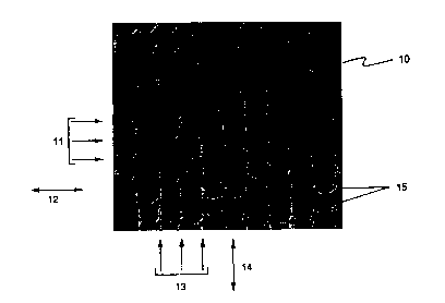
In Figure 3 there is sch~ lly shown a block grating 10. The grating 10
25 includes a series of first ridges 11 e~- .,,l;"g in the direction of the arrow 12 and a series
of second ridges 13 s~ l;ng in the direction of the arrow 14. Ridges 11 and 13 are
generally a,langcd at right angles and provide a mesh pattern of enclosed squares or
rect~ngles. The enclosed squares or l~cl;~ngltos include recesses 15 with the ridges l l and
13 being displaced above the level or levels of the recesses lS. The ridges 11 and 13 in
30 cross section are convex and either or both may have a transverse width less than the
wavelength of the reading light beam. Light striking the ridges 11 and 13 is not reflected
in a conventional manner since the transverse widths of the ridaes 11 and 13 may be less
than the wavelength of the incident light. In this design method, modulation of the block
grating according to the processed diffraction grating data is achieved through modulation
3s of the etched area within each block i.e. within each enclosed area of the mesh pattern.
Hence in Figure 3 each of the recesses 15 has been etched with an area which represents
the processed diffraction grating data value at that point. For example, if the processed
diffraction grating data has been normalised between 0 and 1, then a value of 0.4
in~icat~s that the etched area in the corresponding block should be 40% of the total block
SUBSTITUTE SHEET (RULE 26)
wo 96/07939 . Pcr/Aug5/00542
21 ~9038 14
area. In this block grating design type it is found e~ hicdlly that adjuctrnPnt of the depth
of the etching process can be used to optimise the combination of bri~htnPss andresolution of the resllltin~ dirrlacled images. Increasing the etching depth is found to
produce brighter diffracted irnages ~lthough etching too deeply causes over etching at the
5 top surface of the grating (since the walls of the etched regions are not perfectly
perpen~ir~ r) which results in a loss of resolution in the resulting diffracted images.
Hence there is an op~hllulll etching depth which is deLc,lllined by the plu~cl~ies of the
etching process.
By way of illustration, the spacings b~lwcell ~dj~cPnt ridges in a biock grating of the
10 type illustrated in Figure 3 which is intPn-led for use with red laser light will typically be
in the range 0.5 llliclons to 1 micron, while the ridges 11 and 13 will typically have
widths in at least some portions of tne block grating which are much less than the
wavelength of the light used to view the dirrla~ d images produced by the grating. The
~ro~c.Lies used to replesell~ the processed diffraction grating data within each enclosed
15 area in the mesh pattern of a block grating will typically be de~c.lllilled and etched to an
accuracy of much less than the characteristic (lim~ ion of the block grating - for example
with ~;ullc-llly available technology the positioning accuracy of the features on the grating
is S to 10 nànollh~LI.,s - i.e. around 0.5% to 1% of the side length of an enclosed square
or rect~n~le. However, these figures are illustrative only and should not be regarded as
20 limiting.
An alternative t~chni~e for lccolllillg the processed diffraction grating data is as
modulation on an underlying grating. The underlying grating may for example be aconventional straight line dirrldc-ion grating or may instead be a grating consi~lil1g of
curved lines. In this case the amplitude h~ll,lalion in the processed Fourier Tlah~r(,-ll-
25 can be l~col~ed as the widths of the ulld~.lyhlg grating lines at each point on the etchedplate. The images formed on ill~ ion of the etched plate will occur about the
specular reflection direction for the ill~ beam as well as around each of the
diffraction orders which would normally occur for the umnodulated grating.
It should be appreciated that the present invention does not rely on differences in
30 optical reflectivity or optical transmissivity between the etched and unetched regions of
the optical surface, and that in the plel~l~cd embodiments of the optical surfaces
described herein the surfaces will be uniformly optically reflective or transmissive. For
example in the plcfe..ed embodiment of the surface of Figure 3 the entire optical surface.
including both the ridges 11 and 13 and the recesses 15, will be uniformly optically
35 reflective or llar~lllissi~e. Thus the present invention differs from a number of the
existing methods, such as so-called binary phase holograms, which rely on dirrerences in
reflectivity or transmissivity between treated and u~ eal~d re~ions of the surface.
The etched plate produced using the electron beam lithography m~hinP can be usedsubsequently to produce a commercially viable optically diffractive surface. This surface
SUBSTITUTE SHEET (RULE 26)
WO 96/07939 PCr/AU95/00542
`- 2 1 9933~d -15- . .
may for example be in the form of a thin foil. The process of producing optical foils
from the etched plate preferably involves electroplating of the etched plate to produce a
master shim from which embossing shims are copied. The embossing shims are used to
mPch~nir~lly copy the surface pattern taken from the etched plate into a layer of the foil
5 which is then coated to provide mPch~nir~l protection for the fine embossed structure.
The essenti~l point is that the embossed layer within the foil is ullir(J~ ly optically
reflective or tr~ -ic~i~e, since the embossed surface either begins with the desired
optical reflection or t~ sion chalacl, lisLic or is, after embossing, coated with a layer
of ullirollll optical reflectivity or llal~ll~issi~ity. Suitable illumination of the foil results in
10 production of the diffracted image as from the etched plate. Hence the optical surfaces in
the present invention do not rely on dirr~,el~ces in optical reflectivity or tr~ncmicsivity
bclween the etched and llnPt~hPd regions of the surface. For example in the case of the
crcll~,d embo~imPnt of Figure 3 produced in a silver reflective foil form, the entire
optical dirrlaclion surface, inrln~ing both the ridges 11 and 13 and the recesses 15 are
15 ullirollllly optically reflective. It should be appreciated that other methods, such as an
injection moulding m~tho~, may be used instead for producing commercially viableoptical surfaces from the etched plate.
An advantage of using a block grating design, as illustrated in Figure 3, as opposed
to a mo~lnl~t~d line grating, as described above, is that the block grating enables more
20 llu~r~l;Ci~ Ievels to be iulcol~o,ated into the ploccs~hlg of the Fourier Tlar~ro,lll data and
production of the etched plate. This is because in the case of the block grating the
reflective areas have two variable ~iim~cions rather than only one in the case of the line
gratings. If the electron beam lithography m~rhinP is capable of n quantising levels in the
case of a line grating the same electron beam lithography m~rllinP is capable of n'
2s ~luallliSh~g levels in the case of the equivalent block grating. An increase in the number of
qn~nti.cin~ levels leads to an overall u~ o~,.,lllclll in the quality of the dirrlaclcd image.
Hence, for example, in the case of a block gratin~ it may be possible to use fifty
4..~ levels where less than ten would be possible in the case of the equivalent line
grating. Indeed a typical configuration for a block gratin~ may involve the use of fif~
30 quantising levels to produce clear stable diffracted images.
In the above diccucsed embodiment, the image is described as being projected onto a
screen. In this regard it should be ap~,~.iated that light sensors could be employed to
recognise the image. That is, the image could be specifically tailored (desivned) to be
particularly suitable for machine readability (machine recognisable). This would be
35 particularly advantageous for high security identification and ~llthPntir~tion applications
such as credit cards, personal identification cards and product security.
The above ~liccl~ssed grating could be applied to any article for the purposes of
deterrninin~ the anthPnticity of the article. A gratinC applied to the article would be
..li..AI~d and the image projected on the screen and viewed to determine the
SUBSTITUTE SHEET (RULE 26)
wo 96/07939 Pcr/Auss/00s42
2 1 9903~ -16-
y of the article. ~ltern~tively the image may be pruje~;Led onto an optical
sensor and l"~rhin~ recognised in order to de~ ,~ille the a~lthrntirity of the article. Only
.r~.lir articles would be provided with the grating, as l-n~llthorised reproduction of the
grating would be impossible without access to the above ~liccllcsed method of producing
5 the grating.
In many inct~nres it is beneficial to scale the size of the diffraction image and the
spacing of the diffraction image according to the re~luilellle~ of the application. This
can be done in a straiglllrol~vald manner by scaling the grating pattern produced as
described above. In general reducing the size of the grating pattern will produce larger
10 and more widely spaced images while increasing the size of the grating pattern will
produce smaller more closely spaced images. The relationship belwe~ll the variations in
grating size and the size and spacings of the images are well known according toconventional dirLaclion theory. A particular advantage of reducing the grating size is that
the first order diffraction paLhills can be removed completely. This has the advantage of
OllCellLId~iulg all of the diffracted light into the so-called "zero order" diffracted images
around the specular reflection direction for the illl-,..i.~t;..g beam, thereby making these
images subst~nti~lly brighter. This also has the further advantage of making the image
grating detail considerably more diffir~lt to view via the use of an optical mic~oscope and
Ll-elcrole also conci-l~rably more ~iffirult to copy or COull~-reiL.
Using the techniques described herein it is possible to use a very small gratingpattern to produce totally acceptable and recognisable diffracted images. Typically the
grating paU~ s would occupy a square area having a side length of 0.lmm to 0.5mm in
size, although larger or smaller grating pallcllls may also be used. Also other
configurations may be employed such ac triangular, circular or le.,L~ular. A diffraction
surface as used to ~ a product may be made up of a series of basic grating
pall~lll5 repeated across the surface. Each of these grating l~aLI~lllS rnay be as small as
0.lmm by 0.lmm. If ill.. ;~ rd by a suitably configured and ess~ lly lllonochrolllalic
beam of light the projected diffracted image produced by such a grating pattern is clear
and stable. Such a diffractive surface may be used as described herein to ~..ll,~.,~ir~tr an
30 object.
The optical surfaces described herein are designed to produce specified diffracted
images when suitably illl~lllin~trd, said images being produced around the various
diffraction orders. In particular the diffracted images produced around the specular
reflection direction - the zero order diffraction images - are of interest. In the preferred
35 embodiment illustrated in Figure 3 the optical surface is made up of a regular array of
square or rectangular "cells" defined by the ridges 1 l and 13, with each cell including an
approximately square or rectangular recess 15, where in each cell the widths of the ridges
11 and 13 and the configuration of the recess 15 are delelmilled as described herein.
SUBSTITUTE SHEET (RULE 26)
Wos6/07939 2, 9 9 0 3 8 Pcr/Au95loo542
-17-
The spacings of the ridges 11 and 13, and hence the dimensions of the "cells", in
the surface design of Figure 3 can be specifiPd inrlPpen iPntiy of the angular sizes and
angular positions of the zero order diffraction images produced by the surface of Figure
3. In other words, a number of dirr~"en~ surface designs of the type illustrated in Figure
5 3 could be developed to produce essentially the same zero order diffraction images, with
the various surface designs differing in the spacing~ of the ridges 11 and 13 (and also in
the configurations of the recesses 15).
The angular positions of the higher difflaction orders produced by the surface
design of Figure 3 depend on the spacings of the ridges 11 and 13, with smaller spacings
10 producing larger diffraction angles for the higher diffraction orders.
Hence optical surfaces of the type described herein can be designPd such that the
angular sizes and angular positions of the zero order diffraction images are specified
independently of the angular positions of the higher diffraction orders produced by such
~ulraces.
The present optical surfaces therefore provide a degree of freedom not availablefrom i~ e optical surfaces recorded using conventional holographic tPcl-niqups. In
the case of a holographically recorded surface the angular positions of the various
diffraction orders are specified by the configuration of the recording set-up, and it is not
possible to specify the angular positions of a set of holographic projection images
20 indepen~lently of the angular positions of the higher order images. In the case of the
optical surfaces described herein the ability to specify the angular sizes and angular
positions of the zero order dirrlac~ion images independently of the angular positions of the
higher diffraction orders the,efole provides a means to distinguish the optical surfaces
descli~d herein from illli~ti~e hOlog,aphic surfaces.
Using the techniquPs described herein for ~esigning and ~lod~lc;~-~ diffractive
optical surfaces, and in particular the so-called block grating technique as illustrated in
Figure 3, it is possible to gelle,ale diffracted images which evolve in a specified manner
from one image to another as a specified incident beam of light is moved across an optical
surface. Figure 4 is a scl-Prn~tir illustration of an optical surface 100. The surface 100
30 comprises three regions: the first region 101, the second region 102 and the so-called
transition region 103.
In this yl~r~lled embodiment the optical surface 100, including the regions 101, 102
and 103, is made up of basic units or cells. Figure 5 is a schematic illustration of an area
of the surface 100, showing that the surface 100 is made up of the cells 200. In the
35 present embodiment the cells 200 in the optical surface 100 are all square and all the same
size, although it should be apprecialed that other configurations are possible. Each cell
200 includes an optically diffractive surface design which may preferably be a so-called
block grating design as ~iccu~ed herein. It should be appreciated, however, that optical
surface designs other than a block grating design may be employed in the present
SUBSTITUTE SHEET (RULE 26)
Wo 96/07939 2 1 q 9 0 3 8 Pcr/Auss/00542
-18-
invention. Typically, but not .~PcessA.ily, the cells 200 will have a side length in the
range 0.1 to 0.5mm.
Typically the blocks in the block grating would have a side length (width) of 0.3 to
about 2.0 times the wavelength of the reading light beam. Preferably the width would be
5 0.5 to 1.5 times the wavelength.
Figure 6 illustrates sch~nn~tir~lly the optical propellies of the first and second
regions 101 and 102 of the optical surface 100. The first region 101 is design~d to
produce a first projected image 300 when ill~ d by an appropliate beam of light
301, while the second region 102 is designed to produce a second projected image 302
when similarly illu.. i.-~f~d. The projected images 300 and 302 may be projected onto a
viewing screen for visual verification or onto an optical sensor for m~rllinf verification.
In Figure 6 the images 300 and 302 are shown projected onto a viewing screen 303. The
images 300 and 302 may be any images and will depend on the designs of the optical
su~fares 101 and 102 real,e.Li~ely. The light beam 301 w i!! pre~er..bly be .. Jpecified
15 beam of laser light. At the optical surface the beam will preferably produce a spot of
light having a dimension in the direction of ~,anarolllla~ion of the optical surface - in the
direction of the arrow 304 in Figure 6 - coll.~aldble with the side length of the cells 200.
As the beam of light 301 is moved continuously from the first region 101 across the
transition region 103 to the second region 102, the first projected image 300 will
20 tra~sform into the second projected image 302. Preferably, but not nfcess~-ily, the
.rulllla~ion of the image 300 into the image 302 will be smooth and continuous.
Figure 7 illustrates s~k ..~lir~lly a close-up view of the optical surface 100,
showing a portion of a cell 200. In the present pler~ d embodiment each cell 200inrl~ldec a so-called block grating design (as desclibed herein), wh.~eill the surface of
25 each of the cells 200 is divided into a mesh pattern of enclosed areas or "blocks", which
blocks may preferably be square or l~ ular in shape, or may be some other shape.Each block inrll~des an etched region, resulting in a pit or column, where the plu~e.~ies
(such as area, position and/or depth) of the etched region within the block are specified
according to a prescribed method in order to produce the desired optical effect from the
30 optical surface of the cell, which optical effect in the present invention is the projected
image as shown in Figure 6. For example the specification of the etched region in each
block may be de~ fd using the method described herein. The dimensions of the
features within each block may be less than the wavelength of the incident light beam 301.
For example in the case where each block includes an etched pit, the widths of the ridges
35 ~ulloullding the pit may commonly be less than the wavelength of the light beam 301.
In the ~lcrell~d embodiment illustrated in Figure 7, the block grating within each
cell 200 is made up of a mesh pattern of square enclosed areas or "blocks" 350 with each
block 350 having specified plopellies. In Figure 7 the borders of the blocks 350 are
infljc?~ted by dashed lines which are included for illustrative purposes only - in the design
SUBSTITUTE SHEET (RULE 26)
W096/07939 2 ! ~, 3 3 8 : PcrlAus5/oos42
_19
shown in Figure 7 there is no physical border to each block 350. Each block 350 within a
cell 200 can be specified by its position within the cell, so that for example the (mtn)
block within a particular cell is the mth block from the left and nth block from the bottom
within that cell. To use more precise terminology, each block within a cell can be
5 specified in a Cartesian cooldinate system by its (integer) x and y cooldinates m and n
e.Li~ely within that cell, using the lower left hand corner of the cell as the origin of
the coordinate system. Hence the (m,n) block within one cell has corresponding (m,n)
blocks within all other cells. lt should be a~l reciated that other cell shapes and other
block shapes could be used instead of the square cell and block shapes considered here.
~o In the present embodiment all cells 200 within the first region 101 of the optical
surface 100 are identir~l, and all cells within the second region 102 are identical but
dirrerellt from the cells in the first region 101. The cells in region 101 are design~d to
produce the image 300, while the cells in region 102 are designed to produce the image
302, as illustrated in Figure 6.
The cells 200 in the Iransition region 103 are designed to undergo a prescribed
transformation from the design of the cells in region 101 to the design of the cells in
region 102. Hence as the beam of light 301 is traversed from the first region 101 across
the transition region 103 to the second region 102, the image produced from the beam of
light 301 will transform from the image 300 to the image 302. The image l~allsrollllalion
20 will preferably be smooth, and may be direct (i.e. the image 300 transforms directly into
the image 302) or may involve passing through a number of i..~ te images unliKe
either the image 300 or the image 302.
In the present embodiment the transformation from the cells in region 101 to thecells in region 102 can best be described with the aid of Figures 5 and 7. As illustrated in
Figure 5, in the present embo~limPnt the cells 200 are square and are allanged in a square
layout, altnough it should be a~,piccialed that other configurations are possible. Each of
the cells can be irlPntifil-d by a set of cooldillates (X,Y) where the (X,Y) cell in-lirat~s the
Xth cell from the left and the yth cell from the bottom, as illustrated in Figure S - X and
Y are therefore the (integer) Cartesian coordinates of the cell.
In the transition region 103 all cells with the same X value - i.e. all cells in the same
column - are identical. However, in the transition region 103 cells with different X values
- i.e. cells in dirr~l~nt columns - are different in such a way that the design of a cell
evolves across the transition region from the design of region 101 to the design of re_ion
102.
This can be expressed more precisely as follows.
Consider a particular block (m,n). The y~oy~lies of the (m,n) block will be denoted
P(m,n). These plope.lies may for example include the set of coordinates defining the
"pit" or "column" within the block (m,n) - i.e. the region within the block (m,n) which
has been etched in the process of recording the optical surface 100.
SUBSTITUTE SHEET (RUI E 26)
Wo 96t07939 PcrlAus5loos42
21 99038
-20-
For ;.~ re, Figure 8 is a srh~ "-l;c illustration of a typical block 360 which may
be one of the blocks 350 in Figure 7. In Figure 8 it is ~csumPd that the block 360 includes
an etched region, or "pit", 361, and that both the block 360 and the etched region 361
within the block 360 are square or ~L~n~llar. The block 360 may therefore be specified
5 by the cooldirales [xl,x2,yl,y2,D] which define the re~ion of etching within the block
360, as illustrated, along with the depth of the etched region as r~rescllLcd by the
pclldnlCtel D. In such a configuration the propcl~ies P(m,n) of the (m,n) block may consist
simply of the cOoldillales [xl,x2,yl,y2,D] for the (m,n) block. It should be appreciated,
however, that in some cases additional il~llllaLion, such as the depth profile of the etched
10 region, may also need to be included in specifying the propelLies P(m,n) of the (m,n)
block.
As the X value of the cells increases in traversing the transition region 103, the
plopcllies P(m,n) of the (m,n) blocks within the cells undergo a L~ sr~ll.aLion from the
p~Opcl Lies P1 (~m,n) in the region 101 to ~he properties P2(m,n) in the region 10'
15 accolding to a specified function F. This can be expressed m~l~,r,~lir~lly as:
F {Pl(m,n) ~ P2(m,n)}
In other words, the function F defines the transformation of the ~rope.lies of the
(m,n) block across the tr~mition region 103 from the pro~e.Lies Pl(m,n) in the first
region 101 to the plo~e-lies P2(m,n) in the second region 102.
In the present embo~lim~ntc all cells with the same X value are identir~l and so the
function F is not a function of Y. In other embodim~ntc, however, this may not be the
case.
In the simplest embo~iment, the function F will be a function of the X coordinate of
the cell only, so that all blocks within a cell will undergo the same functional25 Ll~r~llllalion from the plop~ ies of the first region 101 to the propel~ies of the second
region 102.
To take a specific example, the function F may be a linear function of X only,
m~nin~ that the cooldinates [xl,x2,yl,y2,D] for the (m,n) block undergo a lineartlallsro,..-ation as X increases across the transition region 103, starting at the coordinate
30 values for the region 101 and finiching at the coordinate values for the region 102. On the
other hand, the function F may be non-linear. For examplet the function F may be such
that most of the variation in the coordinates [xl,x2,yl,y2,D] for the (m,n) block occurs in
the middle of the transition region 103, or alternatively at either end of the transition
region 103 with little variation in the middle.
In another embodimpnt~ the function F may depend on ~ and also on m and n, so
that dirre.el-l blocks (m,n) within a cell will undergo different functional transformations
from the plop~lies of the region 101 to the propelLies of the region 102. For example.
the blocks in the top right hand corner of the cells may undergo a more strongly non-
linear transformation across the transition region 103 than the blocks in the bottom left
SUBSTlTUTE SHEET (RULE 26)
WO 96/07939 2 i 9 9 0 3 ~ PCI/AU7~ 5~12
-21 -
hand corner of the cells. A depen-lPnre of the function F on the block j-1~ntifi.ors m and n
as well as on the cell column number X may be beneficial in ~en~latillg a particular
optical effect in trar~sro~ g from the image 300 to the image 302.
The function F may either be a continuous function or may be an integer function5 (i.e. for integer values of the variables). However, the variables X, m and n can only take
on discrete values which in the present description are integer values (0, 1, 2, 3, ...).
Hence the function F will be "sampled" only at discrete values of X, m and n.
Whether the function F depends on X only or also on m and n, it should preferably
be chosen so as to produce a smooth looking tlar~follllation from the image 300 to the
image 302 as the beam 301 is traversed from the region 101 across the transition region
103 to the region 102. It may be n~cess~ry to use a non-linear function F to produce a
smooth and continuous looking ~lallsrullllation from the image 300 to the image 302. In
order to ~enelàle smooth image di~ ce and convergence during the image
Llal~rullllation process, it may also be important that the furction F is not strong!y
varying and does not include strong disco,.l;"~ s.
It should be al,prcciated that variations are possible on the plefellcd embodiments of
Figures 4 to 8.
For example, it may be important to provide a projected image which consists of
both a fixed image colllponcll~ and a "llal~rullllillg" image component as described above.
In this case the optical surface 100 could be made up of basic units or cells as described
above, but with each cell Cul~lisillg two separatc sub-cells: a first sub-cell being the
same in all cells and so producing a fixed or co~l~lll projected image from anywhere on
the optical surface; and a second sub-cell being designed acco~ding to the principles
described herein and thc~crule producing an image which kal~ro~ from one specified
image to another as a ~ecified beam of light is traversed across the optical surface.
The image kal~rollllalion process described herein can readily be repeated across a
surface to enable multiple ~.,ccessi~/c ~lu~e~led image L~al~rollllalions as a beam of light is
traversed across the optical surface - i.e. image 1 transforms to image 2, which~lan~rolllls to image 3, and so on.
Similarly, it should be apprcciated that the image 300 and the ima~e 302 above may
actually consist of a number of images, and so the image transformation process described
above may involve multiple first projected irna~es tran~rollllinV into the sarne or a
dirr~lenl number of second projected irnages as a beam of light traverses the optical
surface. (The sim~lt~n~ous production of a number of ima~es from the optical surface 100
can be achieved through applopliate design of the cells 200 as described herein). For
example, the first region 101 in Figure 7 may produce several projected images which
may transform and merge into a single projected image produced by the second region
102.
SUBSTITUTE SHEET (RULE 26)
Wo 96/07939 pcrlAussloos42
21 99038 -22-
Using the Lech~ ues described herein for ~esignino and producing diffractive
optical surfaces, it is possible to ge~ diffracted images which display movementand/or hlL~Ilsily animation effects as a specified incident beam of light is moved across an
optical surface. Figure 9 is a schPm~ti~ illustration of an optical surface 400 desiocned
such that a specified beam of light 401 incident on the surface 400 in a specified manner
results in the production of one or more diffracted beams 402, said diffracted beams 402
producing images 403 when illL~I~;e~L~d by the surfaces 404. The surfaces 404 may be
screens designed to present said images 403 for visual inspection or may be optical
sensors designed to enable m~rhinP recognition of said images 403.
o The surface 400 is designed with varying surface ~ropellies which cause animation
effects in one or more of the images 403 as the incident light beam 401 is moved across
the surface 40Q. The animation effects may for example be movement effects in the
images 403 or illL~nsily animation effects in the images 403. FU1Lh~:1111O1~ the animation
effects may be continuous or disco~inun l5.
Figure 10 illustrates an example 500 of the image 403 of Figure 9, and a movement
animation effect which may be applied to said image 500 through a~ro~,liate design of
the surface 400. In this case the image 500iS an ellipse. The surface 400 may be designed
such that as the light beam 401iS moved across the surface 400 the ellipse 500 rotates in
either a continuous or a discollLilluous manner, as illustrated srhPrn~tir~lly in Figures
10(a) to 10(d). The anim~tion illustrated in the images in Figures lO(a) to lO(d) may
repeat as the light beam 401is moved across the surface 400. It should be appreciated that
the ellipse 500 illustrated in Figure 10 is only one example of an image which may be
produced by the surface 400.
The optical surface 400 could be ~esi~nPd to produce any image or images 403. For
example, the images 403 may be product names or logos which rotate or translate as the
light beam 401 iS moved across the surface 400. In another embo~ the images 403
could be images of people, animals or objects which images move or change shape as the
light beam 401is moved across the surface 400.
Figure 11 illustrates another example 600 of the irnace 403 of Figure 9, and an
illLensily animation effect which may be applied to said image 600. In Figure 11 the image
600 is the word "TEST", although the image 600 could instead be a brand or product
name. The surface 400 may be designed in such a manner that the image 600 is made up
of bright letters (shown in solid shading in Figure 11) and dim letters (shown in outline in
Figure 11), with the combination of bright and dim letters ch~nging as the light beam 401
is moved across the surface 400. For example, Figures 11(a) to 11(d) illustrate a possible
animation effect as the light beam 401 is moved across the surface 400, with a bright
region appea~ g to move through the word TEST in the sequence T, E, S, T as
illustrated. The i,lLensily animation illustrated in the images in Figures 11(a) to 11(d) may
repeat as the light beam 401 is moved across the surface 400.
SUBSTITUTE SH EET (RULE 26)
wo 96/07939 2 1 9 ~ 0 3 8 ~ : PcrlAus5loos42
It should be al)pleciated that more complex h,~ ily animation effects may be
employed. For example, the surface 400 may be designed such that as the beam of light
401 is moved across the surface 400, one or more "waves" of li~ht may move through the
image 403 along a linear, circular or curved path, where the diffracted image 403 could
be any image.
In one l.~efe~led embodiment the surface 400 may be made up of diffractive
elements or cells laid out in a regular manner. Figure 12 illustrates in close-up view a
p,efe.l~d embodiment 700 of the surface 400 illustrated in Figure 9. In Figure 12 the
surface 700 is made up of cells 701 laid out in a square grid as illustrated. It should be
appreciated that other cell shapes and layouts could be used instead. In the embodiment
illustrated in Figure 12 the light beam 401 is configured such that the spot of light 702 at
the surface 400. has approximately the same dimton~ions as a cell 701. Each cell 701 is
designed to produce dirrlaeted beams 402 and diffracted images 403.
The surfase 7Q0 is ~esi~lP~l to produce movement andlor i.lle.~.iLy animation effects
in the images 403 (as descri~ed in relation to Figures 10 and 11) as the light beam 401 is
moved across the surface 700. In the embodiment illustrated in Figure 12 each of the cells
~enelates one "frame" in the animation sequence of the images 403. For example, the
surface 700 may consist of four dirr~e--~ cell types - 703, 704, 705, and 706, with each of
the cell types a.,all~ed in columns as illustrated. It should be al)p.~ciated that other
layouts of the basic cell types 703, 704, 705 and 706 are possible and may be used in
other embo~lim~nt~ to produce additional optical effects.
In one embodiment the surface 700 may be designed to produce the images 500 and
animation effects illustrated in Figure 10, with the cells 703 producing the image
illustrated in Figure lO(a), the cells 704 producing the image illu~ ated in Figure lO(b),
the cells 705 producing the image illustrated in Figure lO(c), and the cells 706 producing
the image illustrated in Figure lO(d). Hence moving the light beam 401 across the surface
in the direction of the arrow 707 will produce the images 500 and animation effects
illustrated in Fi~ure 10. The sequence 703, 704, 705, 706 may be repeated across the
surface 700.
In another embodiment the surface 700 may be desi~ned to produce the images 600
and animation effects illustrated in Figure 11, with the cells 703 producing the imaQe
illustrated in Figure ll(a), the cells 704 producin~ the ima~e illustrated in Fi~ure ll(b).
the cells 705 producin~ the ima_e illustrated in Fi~ure ll(c), and the cells 706 producin~
the image illustrated in Fi~ure ll(d). Hence movin~ the li~ht beam 401 across the surface
700 in the direction of the arrow 707 will produce the images 600 and animation effects
illustrated in Figure 11. The sequence 703, 704, 705, 706 may be repeated across the
surface 700.
In the plefelled embodiment illustrated in Figure 12 where the cell types 703, 704,
705 and 706 are arran_ed in columns, the spot of liCht 70', whether circular or elliptical,
SUBSTITUTE SHEET (RULE 26)
wo 96/07939 2 1 9 ~ 0 3 8 ` PcrlAus5loo542
-24-
will preferably have a dimension p~ ir~ r to the columns (i.e. in the direction of the
arrow 707) which is co~ )alable with or somewhat larger than the tlimon~ion of the cells
in the same direction. The spot of light 702 will preferably have a limonsion in the
direction of the columns - i.e. ~ iru1~r to the direction of the arrow 707 - which is
5 coll,parable with or larger than the dimension of the cells in the same direction. Where
the spot of light 702 is strongly elliptical the long axis of the ellipse will preferably be
parallel to the direction of the columns and said long axis may be .signifir~nt1y longer than
the ~im~onsion of the cells in the same direction. In this way the different diffracted
images from the various cell types will be generated in sequence to produce a smooth
10 animation effect.
Hence the surface 700 incorporates the animation sequence in the form of a series of
diffractive cells recorded across the surface, where each cell produces a "frame" in the
animation sequence. By gel~1a~i"g these "frames" in sequence, the desired animation
effect is pr~duced at the viewing screen 404. In Figure 12 each f:ame is recGrded as a
column of cells, and the animation effect in the diffracted ima~es is produced by moving a
specified beam of light across the surface 700 in a direction approximately p~ ir~ r
to the colurnns of cells, thereby gene,a~ g the animation frames in sequence at the
viewing screen 404. It should be a~ cia~ed, however, that other layouts of cells on the
surface 700 are possible. For example, each frame in the ~nim~tion sequence could be
20 recorded as a single cell, so that a single row of cells produces an animation effect. An
overall anim~tion seql1enre could in this way be recorded in a matrix of cells as a series
of such rows of cells. In this way the overall animation sequence could be played back by
moving the spot of light 702 along one row of cells, then along the adjacent row, and so
on until all cells in the matrix have been sc~nnPd. It should also be appreciated that an
25 ~nim~tion SC.l~le~re could consist of as many frames as desired - for example a 30 frame
sequence, or a 300 frame sequ~nre~ or a 3000 frame sequenre, may be recorded in the
surface 700. It should also be applc. iated that the above described movement and
intensily anim~tion effects may both be illcol~olated into an animation sequenre using the
method described herein. It should be appreciated that the animation techniques described
30 in relation to Figures 9, lO, l l and 12 may also be applied to produce ima~e transformations, or so-called 'morphing', effects.
SUBSTITUTE SHEET (RULE 26)