Note : Les descriptions sont présentées dans la langue officielle dans laquelle elles ont été soumises.
WO 96!07194 PCT/US95109853
- 02199299
1
METHOD OF ELECTROPHOTOGRAPHICALLY
MANUFACTC1R~1G A SCREEN ASSEMBLY
The present invention relates to a method of manufacturing
a luminescent screen assembly for a cathode-ray tube (CRT)
by
. 5 the electrophotographic screening (EPS) process, using
triboelectrically charged screen structure materials, and
more
particularly, to a method for eliminating the misregister
of the
subsequently deposited phosphors caused by the charging
properties of a previously deposited EPS matrix , and for
forming
1 0 a "planarizing" layer that provides a smooth surface for
the screen
assembly.
BACKGROUND OF THE INVENTION
In the electrophotographic screening (EPS) process described
in U.S. Pat. No. 4,921,767, issued to Datta et al., on
May 1, 1990
1 5 and in U.S. Pat. No. 5,229,234, issued to Riddle et al.
on July 20,
1993, dry-powdered, triboelectrically charged, color-emitting
phosphors are deposited, serially, on an electrostatically
chargeable photoreceptor having a dry-powdered, triboelectrically
charged, light-absorbing matrix thereon. The photoreceptor
2 0 comprises an organic photoconductive (OPC) layer overlying,
preferably, an organic conductive (OC) layer, both of which
are
deposited, serially, on an interior surface of a CRT faceplate
panel.
Initially, the OPC layer of the photoreceptor is electrostatically
charged to a positive potential, using a suitable corona
discharge
2 5 apparatus of the type described in U.S. Pat. No. 5,083,959,
issued
to Datta et al. on Jan. 28, 1992. Then, selected areas
of the
photoreceptor are exposed to visible light to discharge
those areas,
without affecting the charge on the unexposed area. Next,
triboelectrically negatively charged, light-absorbing material
is
3 0 deposited, by direct development, onto the charged, unexposed
area of the photoreceptor to form a substantially continuous
pattern of light-absorbing material, hereinafter called
a matrix,
having open areas therein. In order to achieve sufficient
optical
density, oT opacity, of the EPS-deposited matrix, it is
necessary to
3 S build-up a sufficient amount of light-absorbing material.
This,
however, results in a matrix having a relatively rough
surface.
CA 02199299 2002-07-25
-2-
The photoreceptor and the matrix are recharged by the corona discharged
apparatus to impart an electrostatic charge thereon. It is desirable that the
charge
on the photoreceptor be of the same magnitude as that on the previously
deposited matrix; however, it has been determined that the photoreceptor and
the
s matrix do not necessarily charge to the same potential. In fact, the charge
acceptance of the matrix is different from the charge acceptance of the
photoreceptor. Consequently, when different selected areas of the
photoreceptor
are exposed to visible light to discharge those areas, to facilitate reversal
development with triboelectrically positively charged color-emitting phosphor
i o materials, the matrix retains a positive charge of a different magnitude
than the
positive charge on the unexposed area of the photoreceptor. This charge
difference influences the deposition of the positively charged color-emitting
phosphor materials, causing the phosphors to be more strongly repelled by the
charge on the matrix, than by the charge on the unexposed area of the
i5 photoreceptor. This stronger repelling effect of the matrix causes the
color-
emitting phosphors to be slightly displaced from their desired locations on
the
photoreceptor. The repelling effect of the matrix is small, nevertheless, the
effect is sufficient to narrow the width of the color-emitting phosphor lines
so
that the lines do not contact and overlap the edges of the matrix. Thus,
slight
z o gaps occur between the phosphor lines and the surrounding matrix. These
gaps
are unacceptable because they reduce the brightness of the phosphor in each
picture element. Furthermore, the gaps are visible when the screen assembly is
aluminized to provide a reflective backing and anode contact to the screen
assembly.
25 One method of reducing the repulsive effect of the EPS-deposited
matrix is described in U.S. Pat. No. 5,455,132 issued to Ritt et al, on
Oct. 3, 1995. In that application, rather than using an EPS-deposited
matrix, a conventional wet slurry matrix is formed by the process
described in U.S. Pat. No. 3,558,310, issued to Mayaud on Jan. 26, 1971.
3o The conventional matrix is formed directly on the interior surface of
WO 96/07194 PCTIUS95109853
'~ - 02199299
3
the faceplate. The conventional matrix is thin and smooth, and
has the desired opacity so that the OC and OPC layers can be
deposited directly thereon. Additionally, the overlying OC and
OPC layers eliminate the electrostatic interaction between the
matrix and the EPS-deposited phosphors. However, to improve
the efficiency of the screening operation, and to have an entirely
dry screening process, it is desirable also to deposit the matrix by
the EPS process, but without the above-described deleterious
electrostatic interaction.
1 0 A need thus exists to electrically isolate the prior EPS-
deposited matrix so that the matrix is not electrostatically
charged during the EPS deposition of the three color-emitting
phosphors, and to form a planarizing layer that provides a smooth
surface for the subsequent processing of the screen assembly, so
that the phosphors are properly registered with respect to the
matrix.
SUMMARY OF
In accordance with the present invention, a method of
electrophotographically manufacturing a luminescent screen
2 0 assembly on an interior surface of a faceplate panel for a color CRT
comprises the steps of coating the interior surface of the panel
with a volatilizable, organic conductive material to form an organic
conductive (OC) layer, and overcoating the OC layer with a
volatilizable, photoconductive material to form an organic
2 5 photoconductive (OPC) layer. Then, a substantially uniform
voltage is established on the OPC layer, and selected areas of the
OPC layer are exposed to visible light to affect the voltage thereon,
without affecting the voltage on the unexposed area of the OPC
layer. Next, triboelectrically charged, light-absorbing screen
3 0 structure material is deposited onto the unexposed area of the OPC
layer, to form a substantially continuous matrix of light-absorbing
' material having open areas therein. The present method is an
improvement over prior methods in that the present method
includes the additional steps of: forming a planarizing layer on the
3 5 OPC layer; overcoating the planarizing layer with a second coating
of the volatilizable, organic conductive material to form a second
WO 96/07194 PCT/US95109853
-~ 2199299
4
OC layer; and, then, overcoating the OC layer with a second coating
of the volatilizable, organic photoconductive material to form a
second OPC layer.
BRIEF DESCRIPTION OF THE DRAWllVGS
The invention will now be described in greater detail, with
relation to the accompanying drawings, in which:
Fig. 1 is a plan view, partially in axial section, of a color CRT
made according to the present invention;
Fig. 2 is a section as a screen assembly of the tube shown in
1 0 Fig. 1;
Figs. 3 - 8 show a section of a faceplate panel during several
conventional steps in the EPS process;
Fig. 9 is a section of the faceplate panel according to one
embodiment of the novel process; and
Fig. 10 is a section of the faceplate panel made according to a
second embodiment of the novel process.
DETAILED DESCRIPTION OF'~'HE PREFERRED EMBODIMENTS
Fig. 1 shows a color CRT 10 having a glass envelope 11
comprising a rectangular faceplate panel 12 and a tubular neck 14
2 0 connected by a rectangular funnel 15. The funnel 15 has an
internal conductive coating (not shown) that contacts an anode
button 16 and extends into the neck 14. The panel. 12 comprises a
viewing faceplate or substrate 18 and a peripheral flange or
sidewall 20, which is sealed to the funnel 15 by a glass frit 21. A
2 5 three color phosphor screen 22 is carried on the inner surface of
the faceplate 18. The screen 22, shown in Fig. 2, is a line screen
which includes a multiplicity of screen elements comprised of red-
emitting, green-emitting and blue-emitting phosphor stripes R, G,
and B, respectively, arranged in color groups or picture elements
3 0 of three . stripes or triads, in a cyclic order. The stripes extend in a
direction which is generally normal to the plane in which the
electron beams are generated. In the normal viewing position of
the embodiment, the phosphor stripes extend in the vertical
direction. Preferably, at Ieast portions of the phosphor stripes
3 5 overlap a relatively thin, light absorptive matrix 23, as is known
in the art. A dot screen also may be formed by the novel process.
0 21 9 9 2 9 9 pCT~S95/09853
WO 96/07194
A thin conductive layer 24, preferably of aluminum, overlies the
screen 22 and provides means for applying a uniform potential to
the screen, as well as for reflecting light, emitted from the
phosphor elements, through the faceplate 18. The screen 22 and
S the overlying aluminum layer 24 comprise a screen assembly. A
mufti-apertured color selection electrode or shadow mask 25 is
removably mounted, by conventional means, in predetermined
spaced relation to the screen assembly.
An electron gun 26, shown schematically by the dashed lines
in Fig. l, is centrally mounted within the neck 14, to generate and
direct three electron beams 28 along convergent paths, through
the apertures in the mask 25, to the screen 22. The electron gun
is conventional and may be any suitable gun known in the art.
The tube 10 is designed to be used with an external
1 5 magnetic deflection yoke, such as yoke 30, located in the region of
the funnel-to-neck junction. When activated, the yoke 30 subjects
the three beams 28 to magnetic fields which cause the beams to
scan horizontally and vertically, in a rectangular raster, over the
screen 22. The initial plane of deflection (at zero deflection) is
2 0 shown by the line P - P in Fig. 1, at about the middle of the yoke
30. For simplicity, the actual curvatures of the deflection beam
paths, in the deflection zone, are not shown.
The screen is manufactured by the EPS process that is
described in U.S. Pat. No. 4,921,767. Portions of that process are
2 5 shown in Figs. 3 through 8. Initially, the panel 12 is prepared for
the deposition of a light-absorbing matrix 23 by washing the
panel with a caustic solution, rinsing it in water, etching it with
buffered hydrofluoric acid and rinsing it again with water, as is
known in the art. Then, the interior surface of the viewing area
3 0 18 of the faceplate panel 12 is coated with a volatilizable, organic
conductive material to form an organic conductive (OC) layer 32
which provides an electrode for an overlying, volatilizable, organic
photoconductive (OPC) layer 34. The OC layer 32 and the OPC
' layer 34, in combination, form a photoreceptor 36. The faceplate
3 5 structure having the photoreceptor 36 comprising the OC layer 32
with the OPC layer 34 thereon is shown in Fig. 3. Suitable
CA 02199299 2002-07-25
-6-
materials for the OC layer 32 include certain quaternary ammonium
polyelectrolytes recited in U.S. Pat. No. 5,370,952, issued to Datta et al, on
Dec.
6, 1994. The OPC layer 34 is formed of a suitable resin, an electron donor
material, an electron acceptor material, a surfactant and an organic solvent,
s which provide a solution that is overcoated onto the OC layer 32. Examples
of
suitable materials used to form the OPC layer 34 are described in the U.S.
Pat.
No. 5,370,952, issued to Datta et al, on Dec. 6, 1994.
In order to form the matrix 23 by the EPS process, the OPC layer 34 is
electrostatically charged to a suitable potential, within the range of
io approximately +200 to +700 volts, using a corona discharge device 38, of
the
type shown schematically in Fig. 4 and described in U.S. Pat. No. 5,083,959.
Then, the shadow mask 25 is inserted into the faceplate panel 12 and the panel
is
placed onto a three-in-one lighthouse, shown schematically in Fig. 5, as
device
40, that exposes the OPC layer 34 to visible light from a light source 42
which
15 projects light through the openings in the shadow mask. The exposure is
repeated two more times with the light source located to simulate the paths of
the
three electron beams from the electron gun 26 of the tube 10. The light
discharges the exposed areas of the OPC layer 34 where phosphor materials
subsequently will be deposited, but leaves a positive charge on the unexposed
a o area of the OPC layer 34. After the third exposure, the panel is removed
from
the lighthouse and the shadow mask is removed from the panel.
The positively charged area of the OPC layer 34 is directly developed by
depositing thereon triboelectrically negatively charged particles of light-
absorbing material from a developer 44 of the type described in U.S. Pat. No.
25 5,477,285, issued to Riddle et al, on Dec. 19, 1995. Suitable light-
absorbing
material generally contains a black pigment which is stable at a tube
processing
temperature of 450° C. Black pigments suitable for use in making the
light-
absorbing material include: iron manganese oxide; iron cobalt oxide; zinc iron
sulfide; and insulating carbon black. The light-absorbing material is prepared
g g PCT/US95/09853
WO 96/07194
7
by melt-blending the pigment, a polymer and a suitable
charge
control agent that controls the magnitude of the triboelectric
charge imparted to the material, as described in above-referenced
U.S. Pat. No. 4,921,767. A triboelectric gun 46, within
the
S developer 44 provides a negative charge to the light-absorbing
matrix particles. The negatively charged light-absorbing
particles
of matrix material are not attracted to the discharged
areas of the
OPC layer 34, but are attracted to the positively charge
area
surrounding the discharged areas, thereby forming openings
or
windows in the otherwise substantially continuous matrix,
which
the light-emitting phosphors subsequently will overlie.
As
described in the above-cited U.S. Pat. No. 5,229,234, a
second
deposition of matrix material may be made to increase the
opacity
of the matrix. The matrix 23, after development, is shown
in Fig.
1 5 7. For a faceplate panel having a diagonal dimension of
51 cm
(20 inches), the window openings formed in the matrix have
a
width of about 0.13 to 0.18 mm, and the matrix lines have
a width
of about 0.1 to 0.15 mm. As shown in Fig. 8 and described
in the
above-referenced U.S. Pat. No. 4,921,767, the light-absorbing
2 0 material of the matrix 23 is fused to the underlying OPC
layer 34
to prevent movement of the material during subsequent
processing.
In the prior EPS process, described in U.S. Pat. No. 4,921,767,
the matrix-coated faceplate panel is uniformly recharged
to a
2 5 positive potential, re-exposed by passing visible light
through the
apertures in the shadow mask to form a charge image, and
developed with color-emitting phosphors. However, as described
above, the matrix 23, in the prior process, acquires an
electrostatic
potential, during the recharging step, that is different
from, and
3 0 more positive than, the electrostatic potential acquired
by the OPC
layer 34. The higher positive voltage on the matrix 23
repels the
triboelectrically positively charged phosphor particles
so that the
phosphor particles do not completely fill the openings
in the
matrix, but leave small gaps, which are objectionable.
3 5 In order to eliminate these gaps, the matrix 23 must be
electrostatically isolated from the subsequently deposited
WO 96/07194 PCT/US95/09853
-0~'~ 9299
s
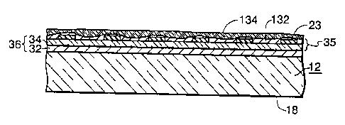
phosphors. This can be achieved by forming a planarizing layer
35 on the OPC layer 34, and then covering the planarizing layer 35
with a second OC layer 132 and a second OPC layer 134. In the
first embodiment of the present method, shown in Fig. 9, the
planarizing layer 35 is not a separate layer, but is formed by the
above-described fusing of the matrix 23 to the OPC layer 34. This
is accomplished by melting the polymer coating on the light-
absorbing matrix material, or by causing the matrix material to be
absorbed into the OPC layer 34 by the fusing operation. Then, the
1 0 planarized layer 35 is overcoated with a second coating of the
same volatilizable, organic conductive coating material, used for OC
layer 32, to form a second OC layer 132. The OC layer 132 is then
overcoated with the same volatilizable, organic photoconductive
coating material, used to form OPC layer 34, to form a second OPC
layer 134. This structure provides sufficient electrical isolation of
the EPS-deposited matrix 23, so that the matrix will not influence
the charge on the second OPC layer 134, during the phosphor
deposition described below.
A second embodiment of the present method is shown in Fig.
2 0 10. The second embodiment is especially useful where the EPS-
deposited matrix 23 has been built-up to provide the required
opacity and has a rough surface that prohibits direct coating of a
continuous OC layer. Then, a separate planarizing layer 135 is
provided over the matrix and the OPC layer 34 by applying a
2 5 filming emulsion of the type marketed under the brand name
RHOPLEX B-74, by the ROHM and HAAS Co., Philadelphia, PA. The
filming emulsion contains a volatilizable resin that can be
removed by baking the screen at a suitable temperature. After
the planarizing layer 135 is formed, the above-described second
3 0 OC layer 132 is overcoated thereon, and then, the OPC layer 134 is
overcoated onto the OC layer 132. The planarizing layer 135
provides a smooth and reasonably level surface on which to form
the second OC layer 132 and the second OPC layer 134 of the
screen assembly, and permits correlation, or register, between the
3 5 matrix 23 and the subsequently deposited color-emitting
phosphors. A possible drawback of the second embodiment is that
CA 02199299 2002-07-25
-9-
an additional quantity of organic filming material is added to the screen
structure
and must be removed during the screen bake step.
Further processing of the of the screen is similar to the prior EPS
practice. The second OPC layer 134 is uniformly electrostatically charged
using
the corona discharge device, described in U.S. Pat. No. 5,083,959, which
charges the second OPC layer 134 to a voltage within the range of
approximately +200 to +700 volts. The shadow mask 25 is then inserted into the
panel 12 and the positively charged second OPC layer 134 is exposed, through
the shadow mask 25, to light from a xenon flash lamp, or other light source of
io sufficient intensity, such as a mercury arc, disposed within the lighthouse
(not
shown). The light which passes through the apertures in the shadow mask 25 at
an angle identical to that of one of the electron beams from the electron gun
of
the tube, discharges the illuminated areas on the second OPC layer 134 on
which it is incident. The shadow mask is removed from the panel 12 and the
i5 panel is placed onto a first phosphor developer (also not shown), but
described
in the above-referenced U.S. Pat. No. 5,477,285. The first color-emitting
phosphor material is positively triboelectrical charged within the developer
and
directed toward the second OPC layer 134. The positively charged first color-
emitting phosphor material is repelled by the positively charged areas on the
a o second OPC layer 134 and deposited onto the discharged areas thereof by
the
process known in the art as "reversal" development. In reversal development,
triboelectrically charged particles of screen structure material are repelled
by
similarly charged areas of the OPC layer 134 and deposited onto the discharged
areas. The size of each of lines of the first color-emitting phosphor is
slightly
25 larger than the size of the openings in the matrix to provide complete
coverage
of each opening, and a slight overlap of the light-absorbing matrix material
surrounding the openings. The panel 12 is then recharged using the above-
described corona discharge apparatus. A positive voltage is established
on the second OPC layer 134 and on the first color-emitting phosphor
CA 02199299 2002-07-25
- 10-
material deposited thereon. The light exposure and phosphor development steps
are repeated for each of the two remaining color-emitting phosphors, with the
light position within the lighthouse, for each exposure, being in accordance
with
the method described in the above-referenced U.S. Pat. No. 5,455,132. The size
s of each of the lines of the other two color-emitting phosphor on the second
OPC
layer 134 also is larger than the size of the matrix openings, to ensure that
no
gaps occur and that a slight overlap of the light-absorbing matrix material
surrounding the openings is provided. The three light-emitting phosphors are
fixed to the second OPC layer 134 in the manner described in U.S. Pat. No.
io 5,474,866 issued to Ritt et al, on Dec. 12, 1995. The screen structure is
then
filmed and aluminized to form the luminescent screen assembly. Due to the high
quantity of organic materials used in the manufacturing of the screen
assembly,
boric acid or ammonium oxalate is sprayed onto the filmed screen structure
before aluminizing, as is known in the art, to provide small openings in the
i s aluminum layer that permit the volatilized organics to escape without
causing
blisters in the aluminum layer. The screen assembly is baked at a temperature
of
about 425°C for about 30 minutes to drive off the volatilizable
constituents of the
screen assembly.