Note : Les descriptions sont présentées dans la langue officielle dans laquelle elles ont été soumises.
SPEClFlCATlOrD 2 1 9 9 89 ~
TITLE
"SOLID-STATE IMAGE SENSING DEVICE, METHOD FOR
DRIVING THEREOF AND CAMERA EMPLOYING THE SAME"
BACKGROUND OF THE INVENTION
Field of the Invention
The present invention relates genera!ly to the field of solid-state image
sensing devices, and more particularly, the present invention relates to an improved
solid-state image sensing device and method of processing image information.
Description of the Related Art
Some solid-state image sensing devices, such as, for example CCD area
sensors, have a structure that includes a drain section 103 for discharging signal
charge and a sweep-out electrode 104 as shown in Fig. 13. These structures are
provided on the side opposite an image section 101 of a horizontal transfer register
102. Application of a sweep out clock ~HOG to the sweep-out electrode 104 for a
given period, sweeps out the signal charges in the horizontal transfer register 102 to
the drain section 103.
On the other hand, some CCD area sensors generally have a horizontal
transfer register 102 with a wide channel width for increasing the capacity for
involved charges because the pitch in the horizontal direction of the horizontaltransfer register 102 is inevitably determined by the number of pixels and the optical
system. In particular, the charge capacity of the horizontal transfer register 102 is
proportional to the area per 1 bit under the condition of constant amplitude of the
transfer clock, and therefore the charge capacity can be increased by increasing the
length and width for one bit. However, the length is limited by the number of pixels
of the image section 101 and only the channel width can therefore be increased.
In a CCD area sensor provided with a horizontal transfer register 102 with a
wide channel width, if the structure for selectively sweeping out the signal charge in
the horizontal transfer register 102 as described herein above is applied, it has been
~2~89~2
difficult to completely sweep out the signal charge within a predetermined time
because the transfer electric field from the horizontal transfer register 102 to the
drain section 103 is weak, particularly the transfer electric field at the middle portion
in the width of the channel is weak when the signal charge in the horizontal transfer
register 102 is intended to be swept out to the drain section 103 through the
sweep-out electrode 104. In order to sweep out the signal charge in the horizontal
transfer register 102, it takes a long time for sweeping out charges, and high speed
sweeping out has been difficult to achieve.
This is true not only for a CCD area sensor having one horizontal transfer
register 102 but also for a CCD area sensor having a structure which includes two or
more horizontal transfer registers such as registers 102a and 102b shown in Fig. 14.
This structure is provided with a transfer electrode 105 between both registers 102a
and 102b in order to independently horizontally transfer and output the signal charge
of two vertical lines for one horizontal period. A drain section 103 and sweep-out
electrode 104 are provided adjacent to the outside horizontal transfer register 102b
in order to selectively sweep out the signal charge in the horizontal transfer registers
~l~a and 102b.
As described herein above, the CCD area sensor having two horizontal
transfer registers 102a and 102b can independently read the signal charge of allpixels of the image section (so-called all pixel reading) by independently reading
signal charge of two vertical lines for one horizontal period. Therefore, the vertical
resolution is improved in comparison with a device that reads signal charges for two
vertical lines which are mixed. For a CCD area sensor of this sort, it is inevitable
that the channel width of each is widened in order to increase the charge capacity of
the horizontal transfer registers 102a and 102b. Thus the residual transfer of signal
charge due to the decrease of the transfer electric field is a problem, as is true for a
CCD area sensor having one horizontal transfer register 102.
This invention is accomplished in view of the above-mentioned problem. One
object of the present invention to provide a solid-state image sensing device capable
of completely sweeping out the signal charge in a horizontal transfer register and for
sweeping out the signal charge to a drain section. Another object of the present
û 2 1 9 9 8 9 i
invention is to provide a device which is capable of high speed sweeping out
operation and a method for driving thereof. Yet another object of the present
invention is to provide a device and method of processing CCD video information
wherein only a portion of the complete image is initially processed at a higher speed
and the remaining portion of the image is stored and later processed or processed
initially at a slower speed. Other objects and advantages of the present invention
will be apparent from the following summary and detailed description of the invention
when viewed in light of the drawings.
SUMMARY OF THE INVENTION
A solid-state image sensing device in accordance with the present invention
has a structure comprising an image section having a plurality of light receivers for
photoelectrically converting incident light to signal charge. A charge transfer section
has a plurality of transfer channels disposed in parallel with each other and a
distribution electrode for distributing the signal charge to each of the plurality of
transfer channels. The device has a multi-channel structure for transferring signal
ch~arge of a full line transferred from the image section. A charge discharging
section is provided adjacent to the side of the charge transfer section opposite to the
image section for selectively sweeping out signal charge in the charge transfer
section.
In the method for driving a solid-state image sensing device in accordance
with the present invention, signal charge is transferred from the image section to the
charge transfer section one line by one line, and the signal charge of one line is
distributed to a plurality of transfer channels in the charge transfer section. Then the
signal charge of one line is transferred in conjunction with the plurality of transfer
channels. Alternatively, the signal charge in the charge transfer section is swept out
to the charge discharging section for a given period.
In the solid-state image sensing device having the structure described herein
above and the method for driving thereof, the channel width of the respective
channels is kept narrow even though the channel width is wide as the whole charge
transfer section. This is regardless of the wide prescription of the channel width for
0 219 9 89 7
the purpose of increasing the charge transfer capacity of the charge transfer section
by providing a plurality of transfer channels to the charge transfer section.
Therefore, the transfer electric field does not decrease when the signal charge is
swept out from the charge transfer section to the charge discharging section, and a
sufficient transfer electric field is obtained. Thus, the signal charge in the charge
transfer section can be swept out to the charge discharging section completely and
quickly.
Additionally, the present invention is directed to providing a solid state imagesensing device which provides video information which is acceptable for use both as
a digital video camera and for providing still images. The present invention satisfies
these demands. The present invention achieves high speed imaging of a selected
portion of an image even without changing the driving speed of the CCD.
BRIEF DESCRIPTION OF THE DRAWINGS
- Fig. 1 is a structural diagram which illustrates one embodiment of the present
invention;
Fig. 2 is a plan pattern diagram of a selected portion of a horizontal transfer
section and charge discharging section;
Fig. 3 is a timing chart illustrating operation of signal charge transfer;.
Fig. 4 is a diagram which illustrates operation of signal charge distribution;
Fig. 5 is a potential diagram during distribution operation of the signal charge;
Fig. 6 is a timing chart during sweep out operation of the signal charge;
Fig. 7 is a diagram for describing the sweep out operation of the signal
charge;
Fig. 8 is a potential diagram during sweep out operation of the signal charge;
Fig. 9 is a set of pick-up image diagram involving the application of the
present invention; (A) is for normal pick-up and (B) is for high speed pick-up;
Fig. 10 is an exemplary image diagram (No. 1) for describing the driving
operation of the application example of the present invention;
Fig. 11 is an exemplary image diagram (No. 2) for describing the driving
operation of the application example of the present invention;
oa-~s~7
Fig. 12 is a structural diagram for illustrating another embodiment of the
present invention;
Fig. 13 is a structural diagram for illustrating one conventional example;
Fig. 14 is a structural diagram for illustrating another conventional example.
Fig. 15 is a diagram which illustrates a camera embodying the presently
claimed invention.
Fig. 16 is a diagram which illustrates a further application of the present
invention.
DETAILED DESCRIPTION OF THE PRESENTLY PREFERRED EMBODIMENTS
Embodiments of the present invention will be described hereinafter in detail
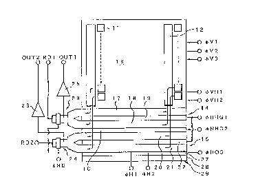
with reference to the drawings. Fig. 1 shows a structural view for illustrating one
embodiment of the present invention. In this embodiment, a CCD area sensor is
provided with, for example, two horizontal transfer registers for improvement of the
vertical resolution.
In Fig. 1, a plurality of light receivers (pixels) 11 comprising, for example,
ph~o-diodes are disposed in the vertical and horizontal directions in matrix
arrangement for converting and storing incident light to signal charge having charge
quantity corresponding to the quantity of light. Vertical transfer registers 12 are
disposed for each vertical line of receiving sections 11. The vertical transfer register
12 comprises a CCD and has, for example, a three layered electrode structure. It is
driven by three-phase vertical transfer clocks ~V1 to ~ V3. Signal charges read
from each receiving section 11 are transferred vertically successively shifting pixels
one by one within a portion of a horizontal blanking period. This is the structure of
the image section.
In the figure, under the image section 13, for example, two horizontal transfer
registers 14 and 15 are provided in parallel. Between the two horizontal transfer
registers 14 and 15, a transfer electrode 16 is located for transferring the signal
charge from the horizontal transfer register 14 to the horizontal transfer register 15.
By applying transfer clock ~ VH1 and UVH2 to the lower two steps (VH1 and VH2)
of each vertical transfer register 12 of the image section 13, signal charge of two
~2~g~897=
vertical lines (two rows) is moved from the image section 13. Two horizontal transfer
registers 14 and 15 comprise CCDs which are two-phase driven using the horizontal
transfer clocks UH1 and UH2. Signal charge for two lines transferred from the
image section 13 is successively transferred in the horizontal direction for a
horizontal scanning period after a horizontal blanking period sharing the signalcharges of one line each.
The horizontal transfer register 14 comprises, for example, two transfer
channels 17 and 18 disposed in parallel and a distribution electrode 19 providedbetween these two transfer channels 17 and 18 for distributing signal charge to each
channel. The device has a multi-channel structure such that the transfer channels
17 and 18 are merged at the output. The horizontal transfer register 14 transfers the
signal charge of the first one line to the horizontal transfer register 15 through the
transfer electrode 16, and transfers the signal charge of the following one line to two
transfer channels 17 and 18 through the distribution electrode 19. The two transfer
channels 17 and 18 transfer horizontally in shared relationship and mix pixels at the
merged output step one by one.
- Similarly, the horizontal transfer register 15 comprises, for example, two
transfer channels 20 and 21 provided in parallel and a distribution electrode 22provided between these two transfer channels 20 and 21 for distributing signal
charge to each channel. It has a multi-channel structure having the two transferchannels 20 and 21 merged at the output. The horizontal transfer register 15
distributes signal charge of one line transferred from the horizontal transfer register
14 through the transfer electrode 16 to two transfer channels 20 and 21 through the
distribution electrode 22, these two transfer channels 20 and 21 transfer horizontally
in sharing relationship and mix pixels at the merged output step one by one.
On the end that is the destination from the horizontal transfer registers 14 and15, for example, charge detectors 23 and 24 having a floating diffusion amplifier
(FDA) structure are provided. The charge detectors 23 and 24 detect the signal
charge transferred horizontally from the horizontal transfer registers 14 and 15 and
convert it to a signal voltage. These signal voltages are output through amplifiers 25
and 26 as CCD outputs OUT 1 and OUT2.
021~9897-
On the opposite side of the outside horizontal transfer register 15 from the
image section 13, a sweep-out electrode 27 and a drain section 28 are provided
adjacent each other along the transfer direction of the horizontal transfer register 15.
The sweep-out electrode 27 and drain section 28 constitute a charge discharging
section 29. By applying a sweep out clock ~ HOG to the sweep-out electrode 27,
the signal charge in the horizontal transfer register 15 and signal charge in the
horizontal transfer register 14 transferred through the transfer electrode 16 and the
horizontal transfer register 15 are swept out to the drain section 28.
In Fig. 2, a plan pattern of a selected portion of the horizontal transfer section
and charge discharging section 29 is shown. In the figure, the transfer electrode 16
and respective distribution electrodes 19 and 22 of the horizontal transfer registers
14 and 15 are respectively formed of the first polysilicon layer (1poly). In thehorizontal transfer registers 14 and 15, a storage electrode 31 is formed of thesecond polysilicon layer (2poly), and a transfer electrode 32 is formed of the third
polysilicon layer (3poly). The storage electrode 31 and transfer electrode 32 which
are disposed adjacent each other in the transferring direction forms a pair. A
c~ bination of two pairs corresponds to one pixel of the image section 13, and
constitutes one bit.
In the horizontal transfer section having such structure, the storage electrode
27 and transfer electrode 28 which form a pair is driven by application of the
horizontal transfer clock ~ H1 and ~ H2 in every other bit. Respective distribution
electrodes 19 and 22 of the horizontal transfer registers 14 and 15 are electrically
connected to each other, and are driven by the same distribution clock ~ HHG1.
The transfer electrode 16 is driven by the transfer clock ~ HHG2. Half-tone dot
meshing zones 33 to 36 in Fig. 2 are channel stop sections.
On the other hand, in the charge discharging section 29, the sweep-out
electrode 27 is also formed of the first polysilicon layer (1 poly) like the transfer
electrode 16 of the horizontal transfer section and respective distribution electrodes
19 and 22 of the horizontal transfer registers 14 and 15. The sweep-out electrode
27 is driven by the sweep out clock ~ HOG. For the sweep out clock ~ HOG, in theexemplary embodiment, a clock with the same phase as of the transfer clock ~
08~Q8~7
HHG2 is used. The storage electrode 27 and transfer electrode 28 of the horizontal
transfer section are formed extending to the portion of the drain section 28 as is
obvious from Fig. 2.
Next, operation of CCD area sensor provided with two horizontal transfer
registers 14 and 15 having multi-channel structure as described herein above is
described. In this CCD area sensor, signal charge of two vertical lines is provided
from the image section 13 to the horizontal transfer registers 14 and 15 for onehorizontal period because two horizontal transfer registers 14 and 15 are provided.
First, the operation for distributing signal charge to each transfer channel of
the horizontal transfer registers 14 and 15 having multi-channel structure is
described based on a timing chart shown in Fig. 3 referring to the operational
description diagram shown in Fig. 4 and the potential diagram in Fig. 5. Fig. 5 is a
potential diagram along the line A-A' in Fig. 4.
As the transfer clock ~ VH2 applied to the gate electrode on the first line rises
to a high level (abbreviated as "H" level hereinafter) during the period from the time
point T1 to the time point T2, the potential under it is deepened. The signal charge
~ marked in Fig. 4) on the first line of the image section 13 is transferred to the
horizontal transfer register 14. Synchronously with this transfer, every signal charge
on lines subsequent to the second line are shifted one line by one line in order, and
thus the signal charge on the second line (o marked in Fig. 4) is transferred to the
pixel train of the first line.
When, the potential of the transfer channels 18 and 21 is shallow because
both horizontal transfer clock ~H2 and distribution clock ~HHG1 are at "H" level, the
potential of the respective transfer channels 17 and 20 of the horizontal transfer
registers 14 and 15 and the potential underthe respective distribution electrodes 19
and 22 is therefore deep. The horizontal transfer clock H1 is in a low level
(abbreviated as "L" level hereinafter). Therefore, the signal charge ~ of the first line
transferred from the image section 13 to the horizontal transfer register 14 is stored
in the transfer channel 17 under distribution electrode 19.
Subsequently, after the transfer clock ~ VH2 changes to "L" level, the
horizontal transfer clock ~H2 changes to "L" level, and the potential of the transfer
0 2 1 99897
channel 17 becomes shallow (time point T3). Then the signal charge in the transfer
channel 17 is transferred under the distribution electrode 19. Thereby, all the signal
charges ~ transferred from the pixel train on the first line of the image section 13 are
stored under the distribution electrode 19. Subsequently, when the transfer clock
~HHG2 becomes "H" level (time point T4), the potential under the transfer electrode
16 becomes deep.
Afterward, the signal charge ~ stored under the distribution electrode 19 is
transferred to the transfer channel 18 under the transfer electrode 16, because when
the horizontal transfer clock ~H1 changes to "H" level, and subsequently the
distribution clock ~ HHG1 changes to "L" level (time point T5), the potential of the
transfer channel 18 becomes deep and the potential under the distribution electrode
19 becomes shallow. Then, when the horizontal transfer clock ~ H1 changes to "L"level and the potential of the transfer channel 18 becomes shallow (time point T6),
the signal charge in the transfer channel 18 is transferred under the transfer
electrode 16, and all the signal charges ~ for a complete one pixel is stored therein.
Next, when the horizontal transfer clock ~H2 changes to "H" level and the
potèntial of the transfer channel 20 of the horizontal transfer register 15 becomes
deep (time point T7), the signal charge ~ stored under the transfer electrode 16disperses from the under transfer electrode 16 to the transfer channel 20. Then,when the transfer clock ~HHG2 becomes "L" level and the potential under the
transfer electrode 16 becomes shallow (time point T8), all the signal charges under
the transfer electrode 16 are transferred to the transfer channel 20, all the signal
charges ~ for full one pixel are stored in the transfer channel 20.
Subsequently, when the distribution clock ~HHG1 changes to "H" level (time
point T9), the potential under the respective distribution electrodes 19 and 22 of the
horizontal transfer registers 14 and 15 becomes deep. Thereby, the signal charge~ stored in the transfer channel 20 of the horizontal transfer register 15 disperses
under the distribution electrode 22. Next, when the transfer clock ~ VH2 applied to
the gate electrode of the first line changes to "H" level and the potential under the
gate electrode becomes deep (time point 10), the signal charge of the first line of the
image section 13 (because this signal charge was the signal charge of the second
02~99897
line, this signal charge is referred to as signal charge of the second line o) is
transferred to the horizontal transfer register 14.
When both the horizontal transfer clock ~ H2 and distribution clock ~ HHG1
are in "H" level, the potential of respective transfer channels 17 and 20 of thehorizontal transfer registers 14 and 15 and the potential underthe respective
distribution electrode 19 and 22 is deep, and the horizontal transfer clock ~ H1 is in
"L" level, the potential of the transfer channels 18 and 21 is therefore shallow. Thus,
the signal charge o of the second line transferred from the image section 13 to the
horizontal transfer register 14 is stored in the transfer channel 17 under the
distribution electrode 19.
Next, after the transfer clock ~ VH2 changes to "L" level and the distribution
clock ~ HH1 changes to the intermediate level (referred to as "M" level hereinafter)
(time pint T11), the potential under the respective distribution electrodes 19 and 22
of the horizontal transfer registers 14 and 15 becomes an intermediate level. The
signal charge which exceeds the storing capacity and overflows is returned to the
transfer channels 17 and 20. Subsequently, the horizontal transfer clock ~ H1
cl~a'~ges to "H" level, and afterward the distribution clock ~ HHG1 changes to "L"
level (time point T12), and the signal charge remaining under the distribution
electrodes 19 and 22 is transferred to the transfer channels 18 and 21.
Through the one series of operations described herein above, the signal
charge ~ o of two vertical full two lines is transferred from the image section 13 to
two horizontal transfer registers 14 and 15. In the respective registers 14 and 15 the
signal charge of each full one line is distributed to the transfer channel 17 and
transfer channel 18, and transfer channel 20 and transfer channel 21 by the
distribution electrodes 19 and 22. Because the horizontal transfer register 14 of the
image section 13 side has a multi-channel structure, if the channel width of thewhole horizontal transfer register 14 for the purpose of increasing the charge
capacity is large, then the width of the respective transfer channels 17 and 18 is still
narrow and the transfer electric field in the channel width direction is sufficient, and
the signal charge of a full one line is transferred from the horizontal transfer register
14 to the horizontal transfer register 15 completely and quickly.
The distributed signal charge is two-phase driven by the horizontal transf~r~
clocks ~ H1 and ~ H2 in the horizontal transfer registers 14 and 15, and horizontally
transferred in sharing with the transfer channels 17 and 18 and transfer channels 20
and 21, and then mixed in a pixel unit at the output step. The signal charge is then
transferred to the charge detectors 25 and 26, converted to a signal voltage therein,
and output as CCD outputs OUT1 and OUT2 for two full lines through the amplifiers
25 and 26.
Next, operation for sweeping outi the signal charge of two full lines of the
image section 13 to the charge discharging section 29 through the horizontal
transfer register 14, transfer electrode 16, and horizontal transfer register 15 is
described based on the timing chart shown in Fig.6. This is done with reference to
the diagram for description of the operation shown in Fig.7 and the potential
diagram shown in Fig. 8. Fig. 8 is the potential diagram along the line B-B' in Fig. 7,
namely the potential diagram from the transfer channel 18 of the horizontal transfer
register 14 to the drain section 28.
The condition at the time point T21 is the same as that of the time point T9
th~t, in the above-mentioned distribution operation of the signal charge. The signal
charge ~ of the first line of the image section 13 is transferred to the horizontal
transfer register 15 through the horizontal transfer register 14 and transfer electrode
16, and stored in the transfer channel 20 under the distribution electrode 22. That
is, up to this point, the signal charge ~ on the first one is transferred to thehorizontal transfer register 15 through the horizontal transfer register 14 and transfer
electrode 16 in the same way as operated in the above-mentioned distribution
operation. The signal charge of the second line is transferred to the horizontaltransfer register 14 and stored in the transfer channel 17 under the distribution
electrode 19.
Next, when the horizontal transfer clock H2 changes to "L" level and the
potential under the transfer channel 20 becomes shallow (time point 22), all thesignal charge ~ of the first line is stored under the distribution electrode 19.Subsequently, when the horizontal transfer clock ~ H1, transfer clock ~
HHG2, and sweep out clock ~ HOG all change to "H" level and the potential of the
transfer channels 18 and 21, the potential under the transfer e~ec~rode 16, and9the
potential under the sweep-out electrode 27 becomes deep (time point T23). Then,
the signal charge ~ of the first line stored under the distribution electrode 19 flows
out to the drain section 28 through the transfer channel 21 under the sweep-out
electrode 27. Then, the signal charge o of the second line stored under the
distribution electrode 19 flows into the transfer channel 18 and under the transfer
electrode 16.
Subsequently, when the distribution clock ~ HHG1 changes to "L" level and
the potential under the distribution electrode 19 becomes shallow (time point T24),
the signal charge ~ of the first line stored under the distribution electrode 22 is
completely swept out to the drain section 28, and the signal charge of the second
line stored under the distribution electrode 19 is completely transferred to thetransfer channel 18 and the transfer electrode 16. Then, when the horizontal
transfer clock ~ H1 changes to "L" level and the potential of the transfer channels 18
and 21 become shallow (time point T25), the signal charge of the second line is
completely stored under the transfer electrode 16.
- Next, when the horizontal transfer clock ~ H2 and distribution clock ~ HHG1
change to "H" level and the potential of the transfer channels 17 and 20 and thepotential under the distribution electrodes 19 and 22 becomes deep (time point T26),
the signal charge o of the second line stored under the transfer electrode 16 flows
into the transfer channel 20 of the horizontal transfer register 15 under the
distribution electrode 22.
Then, when the transfer clock ~ HHG2 and sweep out clock q, HOG change
to "L" level and the potential under the transfer electrode 16 becomes shallow (time
point T27), the signal charge of the second line stored under the transfer electrode
16 flows into the transfer channel 20 of the horizontal transfer register 15 under the
distribution electrode 22. When the horizontal transfer clock ~ H2 changes to "L"
level and the potential of the transfer channels 17 and 20 become shallow (time
point T28), all the signal charge o of the second line is stored under the distribution
electrode 22. This condition is the same as that at the time point T22, and after this
point in time, the signal charge o of the second line is swept out to the drain section
12
~ ~ ~ 9 9 89 ~
by repeating the same operation as that after the time point T22.
By the above-mentioned series of operations, the signal charge of each pixel
of the image section 13 is swept out in a unit of a line to the drain through the
horizontal transfer register 14, transfer electrode 16, horizontal transfer register 15,
and sweep-out electrode 27. Because the horizontal register 14 employs a
multi-channel structure as described hereinbefore, the signal charge for full one line
can be completely transferred from the horizontal transfer register 14 to the
horizontal transfer register 15. Further, because the horizontal register 15 employs
also the multi-channel structure, if the channel width of the whole horizontal transfer
register 15 is designed to be wide for the purpose of increasing the charge capacity,
the channel width of the respective transfer channels 20 and 21 is still narrow and
the transfer electric field in the channel width direction is sufficient. Therefore the
signal charge for a full one line can be transferred completely and speedily from the
horizontal transfer register 15 to the drain section 28.
By driving the sweep-out electrode 27 with the clocks (~ HHG2 and ~HOG)
having the same phase as the transfer electrode 16 between the horizontal transfer
regi~sters 14 and 15, the sweep out operation of the signal charge from the horizontal
transfer register 15 to the drain section 28 and the transfer operation of the signal
charge from the horizontal transfer register 14 to the horizontal transfer register 15
are operated simultaneously. Therefore, time is saved, and the discharging
operation of the signal charge in the unit of a line is possible. Only one driver is
sufficient because the transfer clock ~ HHG2 and sweep out clock ~ HOG are driven
with the same phase.
The operation is described referring to an example in which the signal charge
of each pixel of the image section 13 is swept out to the drain section 28 in the
above-mentioned operation description, however, it may be possible that after the
signal charge is horizontally transferred in a certain period of time for a horizontal
effective period from the horizontal transfer registers 14 and 15, then the residual
signal charge in the horizontal transfer registers 14 and 15 is swept out to the drain
section 28 through the same operation as that described above.
Next, an operative example of the CCD area sensor having the multi-channel
0 2 ~ ~ 9 89 7
structure as described herein above and provided with two horizontal transfer
registers 14 and 15 will be described. This is an example where the left lower half of
the image section 13 (1/4 of effective pixels) is sectioned, and one picture is
obtained within 1/4 the usual time, thereby, driving with four times the picture rate is
possible. Fig. 9 is an image diagram involving this application example, (A) shows a
normal pick-up and (B) shows a high speed pick-up in which 1/4 of the area (o) is
sectioned.
The driving operation in this operative example is described with reference to
the operation image shown in Fig. 10 and Fig. 11. In this operative example, thenumber of vertical lines is 15 is described. Because the pick-up image on the image
section 13 is mirror symmetrical with the actual regenerated image, after the line
number R is added for the lines on the left half of the effective pixel area, L is added
for the lines on the right half.
Assuming that the left lower half of the effective pixel area enclosed with a
thick line in Fig. 10(A) is the area where the lines 1R to 7R are used, first, the signal
charge 1 R, 1 L on the first line is transferred to the horizontal transfer register 14 as
sllown in Fig. 10(B). Subsequently, the signal charge 1 R, 1 L of the first line on the
horizontal transfer register 14 is transferred to the horizontal transfer register 15 as
shown in Fig. 10(C), and simultaneously the signal charge 2R, 2L of the second line
is transferred from the image section 13 to the horizontal transfer register 14.From this condition, the horizontal transfer registers 14 and 15 are driven for
horizontally transfer during a half of the normal interval. Thereby, the signal charge
1 R, 2R of the first line and second line of the left half of the effective pixel area is
output as CCD outputs OUT1 and OUT2. The signal charge 1 L of the first line andthe signal charge 2L of the second line on the right half of the effective pixel area is
residual on the left half of the horizontal transfer registers 15 and 14 as shown in
Fig. 10(D).
Next, the respective signal charges 1 L, 2L of the first line and the second line
remaining residually on the left half of the horizontal transfer registers 14 and 15 are
swept out to the charge discharging section 29. In particular, first the signal charge
1 L of the first line remaining residually on the horizontal transfer register 15 is swept
14
8 ~ ~
out to the charge discharging section 29. Then, as shown in Fig. 11 (A), the signal
charge 2L of the second line remaining residually on the horizontal transfer register
14 is transferred to the horizontal transfer register 15, and the signal charge 3R, 3L
of the third line is transferred from the image section 13 to the horizontal transfer
register 14 .
Subsequently, the signal charge 2L of the second line transferred to the
horizontal transfer register 15 is swept out to the charge discharging section 29.
Then as shown in Fig.11 (B), the signal charge 3R, 3L of the third line of the
horizontal transfer register 14 is transferred to the horizontal transfer register 15, and
simultaneously to the horizontal transfer register 14, the signal charge 4R, 4L of the
fourth line is transferred. Thereafter, the signal charge 3R, 3L of the third line and
the signal charge 4R, 4L of the fourth line are read and swept out. By repeating the
above-operation up to the seventh line that is the uppermost line in the used area,
only the signal charges 1 R to 7R in the used area are output as signals.
After completing respective operations of reading and sweeping out of the
signal charge in the used area, reading from the signal charge 8R, 8L of the eighth
lirré'ls not performed, all the signal charges from the signal charge of 8R, 8L to the
signal charge of 15R,15L of the fifteenth line are swept out to the charge
discharging section 29. The condition in this process is shown in Fig. 11 (C). This
figure shows the condition where the signal charge 8R, 8L of the eighth line is swept
out to the charge discharging section 29, the signal charge 9R, 9L of the ninth line is
transferred to the horizontal transfer register 15, and the signal charge 10R, 10L of
the tenth line is transferred to the horizontal transfer register 14.
When the signal charge 15R,15L of the fifteenth line is swept out to the
charge discharging section 29, reading and sweeping out of the signal charge of all
pixels for full one picture are completed as shown in Fig.11 (D). By performing the
series of operations described above, the transfer operation of a CCD area sensor
can be performed within 1/4 of the normal time interval, and the picture rate can be
increased by four times. This is the operation that can be only realized by using the
horizontal transfer registers 14 and 15 both having the multi-channel structure as
described hereinbefore in order to completely transfer the signal charge to the
charge discharging section 29. a a ~ ~ q ~ ~ ~
In the above-mentioned embodiment, the application of a CCD area sensor
having two horizontal transfer registers 14 and 15 are described, however, the
present invention is by no means limited to this case. The present invention is
applied to a CCD area sensor having one horizontal transfer register and having a
charge discharging section adjacent to it. In the case of this CCD area sensor, by
structuring one horizontal transfer register to 6 multi-channel, if the channel width of
the whole horizontal transfer register is widened for the purpose of increasing the
charge capacity, the signal charge in the horizontal transfer register (including the
signal charge just after the transfer from the image section to the horizontal transfer
register) still can be swept out completely and speedily because each channel width
of respective transfer channels is still narrow and the transfer electric field in the
channel width direction is sufficient.
The present invention is also applied to a CCD area sensor having three or
more of horizontal transfer registers in the same way. Fig. 12 is a structural diagram
which illustrates the application of the present invention to a CCD area sensor
hâ~vlng, for example, three horizontal transfer registers, the same components in the
Fig.12 as in Fig.1 are provided with the same number as in Fig.1. In this
embodiment, the third horizontal transfer register 31 is provided outside the second
horizontal transfer register 15 with interposition of the transfer electrode 30. The
charge discharging section 29 is provided adjacent to the out side of the horizontal
transfer register 31.
The third horizontal transfer register 31 comprises, for example, two transfer
channels 32 and 33 disposed in parallel and a distribution electrode 34 providedbetween these two transfer channels 32 and 33 for distributing the signal charge to
each channel like the horizontal transfer registers 14 and 15. This structure includes
the multi-channel structure having the transfer channels 32 and 33 merged at theoutput. The horizontal transfer register 31 distributes the signal charge for a full one
line transferred from the horizontal transfer register 15 through the transfer electrode
30 to two transfer channels 32 and 33 using the distribution electrode 34. The
charge transfer is horizontally transferred by way of two transfer channels 32 and 33
16
in sharing relationship and charges are mixed at the merged outp!~. 2 ~ ~ ~ fl 9At the destination end of the horizontal transfer register 31, a charge detector35 having, for example, a floating diffusion amplifier structure is provided. The
charge detector 35 detects the signal charge transferred through the horizontal
transfer register 31 and converts it to a signal voltage. The signal voltage is output
as a CCD output OUT3 with two other CCD outputs OUT1 and OUT2 through the
amplifier 36.
In the CCD area sensor provided with three horizontal transfer registers 14,
15, and 31 each of which has the multi-channel structure, the respective distribution
electrodes 19, 22, and 34 of the horizontal transfer registers 14, 15 and 31 areelectrically connected to each other, and driven by the same distribution clock
HHG1. The transfer electrodes 16 and 30 provided between the horizontal transferregisters 14, 15, and 31 are aiso electrically connected each other, and driven by the
same transfer clock ~HHG2.
As described herein above, in the CCD area sensor having three horizontal
transfer registers 14, 15, and 31 provided with the charge discharging section 29
a-djà~cent to the outermost horizontal transfer register 31, by employing the
multi-channel structure for all three horizontal transfer registers 14, 15, and 31, the
channel width of each transfer channel can be still suffficiently narrow and thetransfer electric field in the channel width direction can be suffficient. Therefore the
signal charge in the horizontal transfer registers 14, 15, and 31 (including just after
the transfer from the image section 13 to the horizontal transfer register 14, transfer
to the horizontal transfer register 15 through the horizontal transfer register 14, and
transfer to the horizontal transfer register 31 through the horizontal transfer registers
14 and 15) can be swept out completely and speedily.
The respective distribution electrodes 19, 22, and 34 of the horizontal transferregisters 14, 15, and 31 are driven intentionally by the same distribution clock~HHG1, and it is not necessary to differentiate the distribution clock ~HHG1
between the respective registers regardless of the increase in the number of thehorizontal transfer registers having the multi-channel structure or the number of
channels, and the same structure as the driving system is used as it is. Similarly,
n a~ 9 7
the use of the same transfer clock ~ HHG2 for driving the transfer electrodes 16 and
30 between the horizontal transfer registers 14, 15, and 31 eliminates the necessity
of the transfer clock ~ HHG2 change regardless of the number of the horizontal
transfer registers, and the same structure as the driving system is used.
In this embodiment, the CCD area sensor having three horizontal transfer
registers 14, 15, and 31 is described. However, needless to say, the present
invention can be applied in the same manner to a CCD area sensor having four or
more horizontal transfer registers and provided with a charge discharging section
adjacent to the outermost horizontal transfer register. As described herein above,
by employing the structure that uses the same distribution clock ~HHG1 for driving
all the respective distribution electrodes of the horizontal transfer registers and that
uses the same transfer clock ~HHG2 for driving all the respective transfer electrodes
between the horizontal transfer registers, it is advantageous that there is no need to
change the structure of the driving system regardless of the increase in the number
of horizontal transfer registers.
As described herein above, according to the present invention, a solid-state
,~~
image sensing device is provided with at least one charge transfer section for
transferring signal charge transferred from the image section and a charge
discharging section disposed adjacent to the side of the charge transfer sectionopposite to the image section. The charge transfer section has a multi-channel
structure, thereby each channel of respective transfer channels can be narrow
regardless of the channel width of the whole charge transfer section for the purpose
of the increasing charge capacity. Signal charge can be swept out to the charge
discharging section completely and speedily because the transfer electric field is
sufficient for sweeping out the signal charge from the charge transfer section to the
charge discharging section.
Figure 15 is a block diagram illustration of a camera embodying the present
invention. The camera is shown generally at reference 201. An optical unit 203
receives light and focuses the incident light on an imaging section 205. The imaging
section receives the incident light and a plurality of pixels such as those disclosed
with reference to Figure 1 convert the light to charge. The imaging section is
18
9 7
attached to a processing unit 206 which processes the selected or desired pixels as
described in more detail above. An operator is able to select high speed processing
for a particular portion of the image by depressing a select switch on the camera
unit.
Rather than sweeping away the charges into a discharge unit, it has been
recognized that the charges can be further transferred into an additional horizontal
transfer unit rather than being discharged and lost. Figure 16 illustrates such a
device. In Figure 16, a secondary horizontal transfer unit 220 is placed adjacent and
a transfer electrode which is used to transfer the electric charges from the primary
horizontal transfer registers 222 and 223. In a high speed imaging mode, rather
than simply sweeping out the undesired portion of signal charges, the signal charges
are initially transferred to the secondary horizontal transfer register 220.
It is further recognized that the secondary horizontal transfer register could
actually be comprised of one or more secondary horizontal transfer registers
depending on the particular design. The secondary horizontal transfer registers feed
a further processing unit 227.
,~
- The further processing unit 227 includes a charge voltage converter as is
known in the art for converting pixel charges to voltages. The voltages may then be
either stored in a memory associated with the further processing unit 227 or they
may be immediately processed into additional video information.
Advantageously, the further processing unit may operate at a slower speed in
order to conserve battery power or to allow the primary processor to more quickly
process a desired image portion. Significantly, the image information which is not
processed immediately may be later combined with the initially desired image
information to provide a composite image. The system identifies which portion of the
image has been selected for initial processing and which has been transferred to the
secondary image processing unit 227. Thus, through maintaining this information,the imaging devices are able to later recombine the image information into a
composlte image.
19