Sélection de la langue

Search

Sommaire du brevet 2200122 

Énoncé de désistement de responsabilité concernant l'information provenant de tiers

Une partie des informations de ce site Web a été fournie par des sources externes. Le gouvernement du Canada n'assume aucune responsabilité concernant la précision, l'actualité ou la fiabilité des informations fournies par les sources externes. Les utilisateurs qui désirent employer cette information devraient consulter directement la source des informations. Le contenu fourni par les sources externes n'est pas assujetti aux exigences sur les langues officielles, la protection des renseignements personnels et l'accessibilité.

Disponibilité de l'Abrégé et des Revendications

L'apparition de différences dans le texte et l'image des Revendications et de l'Abrégé dépend du moment auquel le document est publié. Les textes des Revendications et de l'Abrégé sont affichés :

  • lorsque la demande peut être examinée par le public;
  • lorsque le brevet est émis (délivrance).
(12) Brevet: (11) CA 2200122
(54) Titre français: ENSEMBLE A PASTILLE PRINCIPALE POUR COMPOSANTS MONTES EN SURFACE
(54) Titre anglais: UNI-PAD SURFACE MOUNT COMPONENT PACKAGE
Statut: Périmé et au-delà du délai pour l’annulation
Données bibliographiques
(51) Classification internationale des brevets (CIB):
  • H05K 3/32 (2006.01)
  • H05K 1/00 (2006.01)
  • H05K 1/11 (2006.01)
  • H05K 3/34 (2006.01)
(72) Inventeurs :
  • NIKMANESH, KHALIL N. (Etats-Unis d'Amérique)
  • SMITH, DOUGLAS JAY (Etats-Unis d'Amérique)
(73) Titulaires :
  • LUCENT TECHNOLOGIES INC.
(71) Demandeurs :
  • LUCENT TECHNOLOGIES INC. (Etats-Unis d'Amérique)
(74) Agent: KIRBY EADES GALE BAKER
(74) Co-agent:
(45) Délivré: 2001-10-30
(22) Date de dépôt: 1997-03-17
(41) Mise à la disponibilité du public: 1997-10-18
Requête d'examen: 1997-03-17
Licence disponible: S.O.
Cédé au domaine public: S.O.
(25) Langue des documents déposés: Anglais

Traité de coopération en matière de brevets (PCT): Non

(30) Données de priorité de la demande:
Numéro de la demande Pays / territoire Date
634,486 (Etats-Unis d'Amérique) 1996-04-18

Abrégés

Abrégé français

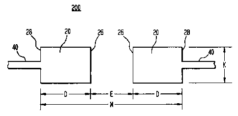
Structure à pastille principale à la surface d'une carte imprimée comprenant une paire de pastilles complémentaires disposées sur un axe, dont les dimensions sont choisies de manière à pouvoir recevoir les bornes de composants montés en surface ayant des dimensions variées. La largeur de chaque pastille est celle du composant monté en surface le plus large prévu qui peut être substitué. Une première distance, marquant la séparation des bords intérieurs de chaque pastille, est choisie comme distance minimale entre les bords intérieurs des bornes des composants montés en surface prévus. Une deuxième distance, marquant la distance entre les bords extérieurs des pastilles complémentaires est choisie comme distance maximale entre les bords extérieurs des bornes des composants montés en surface prévus. Les tolérances de fabrication peuvent être intégrées à chacune de ces dimensions. Il y a aussi une description du procédé de fabrication qui tient compte des dimensions des composants montés en surface qui sont susceptibles d'être substitués à d'autres et des tolérances de fabrication qui peuvent être ajoutées aux dimensions de la pastille principale ou en être retranchées.


Abrégé anglais


A uni-pad structure on the surface of a PWB
comprising a pair of complimentary pads, arranged on an
axis, whose dimensions are selected to support the
terminals of a plurality of surface mount component
sizes. The width of each pad is the width of the widest
anticpated surface mount component which may be
substituted. A first distance, denoting the separation
of the inner edges of each pad, is selectd as the minimum
distance between inner edges of the terminals of the
anticipated surface mount components. A second distance,
denoting the distance between outer edges of the
complimentary pads is selectd as the maximum distance
between outer edges of the terminals of anticipated
surface mount components. A second distance, denoting
the distance between outer edges of the complimentary
pads is selected as the maximum distance btween outer
edges of the terminals of anticipated surface mount
components. Manufacturing tolerances may be incorporated
into each of these dimensions. A design process is
described which considers the dimensions of surface mount
components which are likely to be substituted and
manufacturing tolerance which may be added to or
substracted from the dimensions of the uni-pad.

Revendications

Note : Les revendications sont présentées dans la langue officielle dans laquelle elles ont été soumises.


8
Claims:
1. In a printed circuit board capable of receiving surface
mount devices of different sizes between a minimum and a
maximum, wherein each surface mount device has an electrical
component with a length ranging between a minimum length and a
maximum length and a width ranging between a minimum width and
a maximum width, said electrical component being bounded by
conductive end portions having a minimum length and a maximum
length and sharing the same width as the electrical component,
a bonding pad for bonding the surface mounted device to the
printed circuit board, comprising:
two conductive pads spaced a predetermined distance
apart, each of said pads having a single uniform length and a
single uniform width, wherein a sum of said predetermined
distance plus said length of each of said pads is generally
equal to the sum of the maximum length of the electrical
component plus the maximum length of each of the conductive
end portions, and said width of said pads is generally equal
to the maximum width of the conductive end portions.
2. The bonding pad of claim 1 wherein each of said
conductive pads is solder coated.
3. The bonding pad of claim 1 further comprising at least
one electrical trace emanating from each of said conductive
pads.
4. A method of manufacturing a printed circuit board capable
of receiving surface mount devices of different sizes between
a minimum and a maximum wherein each surface mount device has
an electrical component with a length ranging between a
minimum length and a maximum length and a width ranging

9
between a minimum width and a maximum width, said electrical
component being bounded by conductive end portions having a
minimum length and a maximum length and sharing the same width
as the electrical component, said method comprising the steps
of:
producing a printed circuit board having a plurality of
positions for receiving surface mount devices;
placing two conductive pads at each of said positions,
each of said pads having a single uniform length and a single
uniform width and being spaced a predetermined distance apart
wherein a sum of said predetermined distance plus said length
of said pads is generally equal to the sum of the maximum
length of the electrical component plus the maximum length of
each of the conductive end portions, and said width of said
pads is generally equal to the maximum width of the conductive
end portions.
5. The method of claim 4 further comprising:
adding a manufacturing tolerance to said width of each of
said pads.
6. The method of claim 4 further comprising the steps of
subtracting a manufacturing tolerance from the sum of the
predetermined distance plus the length of each of the
conductive pads.
7. The method of claim 4 further comprising the steps of
adding an amount to said predetermined distance sufficient to
compensate for the surface tension force associated with
molten solder.
8. The bonding pad according to claim 1 wherein the surface
mount device has manufacturing tolerances and said

10
manufacturing tolerances are included in the maximum length
and maximum width of the electrical component.
9. The bonding pad according to claim 1 wherein said
predetermined distance is generally equal to the minimum
length between the conductive end portions.
10. The bonding pad according to claim 1 wherein said
predetermined distance is generally equal to the minimum
length between the conductive end portions plus a constant.
11. The bonding pad according to claim 10 wherein said
constant is an empirically determined amount that is
calculated to prevent the surface mount device from raising
off of the printed circuit board during a soldering process.
12. The bonding pad according to claim 10 wherein said
constant is up to six mils.
13. A printed circuit board assembly capable of receiving
surface mount devices of different sizes between a minimum and
a maximum, wherein each surface mount device has an electrical
component with a length ranging between a minimum length and a
maximum length and a width ranging between a minimum width and
a maximum width, said electrical component being bounded by
conductive end portions having a minimum length and a maximum
length and sharing the same width as the electrical component,
said printed circuit board assembly, comprising:
a printed circuit board having a plurality of positions
dedicated for receiving surface mounted devices;
two conductive pads at each of said positions, each of
said pads having a single uniform length and a uniform width
and being spaced a predetermined distance apart, wherein a sum

11
of said predetermined distance plus said length of each of
said pads is generally equal to the sum of the maximum length
of the electrical component plus the maximum length of each of
the conductive end portions, and said width of said pads is
generally equal to the maximum width of the conductive end
portions.
14. The assembly according to claim 13 wherein the surface
mount device has manufacturing tolerances and said
manufacturing tolerances are included in the maximum length
and minimum length of the electrical component, the maximum
width and minimum width of the electrical component and the
maximum length and the minimum length of the conductive end
portions.
15. The assembly according to claim 13 wherein said
predetermined distance is generally equal to the minimum
length between the conductive end portions.
16. The assembly according to claim 13 wherein said
predetermined distance is generally equal to the minimum
length between the conductive end portions plus a constant.
17. The assembly according to claim 16 wherein said constant
is an empirically determined amount that is calculated to
prevent the surface mount device from raising off of the
printed circuit board during a soldering process.

Description

Note : Les descriptions sont présentées dans la langue officielle dans laquelle elles ont été soumises.


,_ 2200122
UNI-PAD FOR SURFACE MOUNT COMPONENT PACKAGE
Field of the Invention
This invention relates to electrical component
surface mount technology, and in particular to the
bonding pads on printed wiring boards which support the
components.
Descriution of Related Art
The design and use of printed wiring boards, PWBs,
is a well known art because it provides for lower labor
cost, increased standardization, higher reliability, and
greater packing density than hard wired circuitry.
Initially, this was a through-hole technology to
accommodate pig-tailed discrete components such as
resistors, capacitors, inductors, and transistors which
were then prevalent and which were designed for hard
wiring. The leads emanating from each component were
bent, inserted through the holes in the PWB, and soldered
to terminal pads on the other side of the PWB. The
soldering was by hand or by skimming the lower surface of
the PWB over a solder bath. This technology provided
tremendous advantages over point-to-point wiring, but it
still used a relatively large area because the discrete
components were essentially designed for point-to point
wiring assembly.
Surface mount technology provided discrete
components designed for the automated assembly of PWBs.
They were smaller, and, more importantly, their external
contacts were made integral with the body of the
component. They were a rectangular solid rather than
cylindrical, and were specifically made for pick-and-
place assembly and reflow soldering. In the assembly
process, a solder paste is screened by a squeegee through
a stencil, typically stainless steel, which has
photolithographically defined holes which correspond to
pad areas on the PWB. The solder paste is a mixture of

2200122
2
solder particles of predetermined composition and melting
point. The particles are contained in a viscous medium
of soldering flux, solvent, and viscousifiers or other
agents which improve the screening operation and provide
a tacky surface onto which the terminals of the surface
mount component are set. The components are usually
presented in a tape or cartridge and a programmed pick-
and-place machine lifts them from their container with a
vacuum chuck, orients and aligns them over the correct
pads, and places them onto the soldering paste. The
viscous flux holds the components in place over the pads
which are typically solder coated copper. The terminals
on each end of the surface mount component are also
solder coated and the flux in the paste dissolves any
oxide which may be present and ensures that the solder
particles will wet the component terminals and their
corresponding pads. This reflow process is done in an
oven and the solder is usually a tin-lead alloy, near the
eutectic composition, which melts at 183 degrees
centigrade. Other alloy compositions can be used to melt
at different temperatures which are well known in the
art.
Surface mount components are manufactured in a set
of standard sizes, and the pads that support their
terminals are designed for each particular type and size.
Once a design is in production and an inventory of
surface mount PWBs is accumulated, any changes in design
become very costly and time consuming. These changes
occur due to design changes to improve performance or
reliability or the need to change suppliers because of
availability and price. Changes to reduce cost may be
thwarted by the increased cost of redesigning the PWB.
Changes for the sake of availability or performance are
slowed because new PWBs need to be designed and made. In
many cases, the new designs must be re-certified for
U.L., CSA, etc.

zzoo ~ zz
3
Accordingly, there is a need in the art of surface
mount technology for a PWB with pads that accommodate
surface mount components of varying dimensions so that
components may be interchanged to take advantage of
better price/availability or to improve performance and
reliability without the expense, delay and risk to other
design areas of PWB redesign and manufacture.
Summary Of The Invention
The present invention relates to a uni-pad which is
a structure on the surface of a PWB comprising a pair of
complimentary pads, arranged on an axis, whose dimensions
are selected to support the terminals of a plurality of
surface mount component sizes. The width of each pad is
the width of the widest anticipated surface mount
component which may be substituted. A first distance,
denoting the separation of the inner edges of each pad,
is selected as the minimum distance between inner edges
of the terminals of the anticipated surface mount
components. A second distance, denoting the distance
between outer edges of the complimentary pads is selected
as the maximum distance between outer edges of the
terminals of anticipated surface mount components. A
manufacturing tolerance may be incorporated into each of
these dimensions. The most critical of these is the
first distance between the inner edges of complimentary
pads where a manufacturing tolerance may be subtracted
from that distance. For the second distance between the
outer edges of the complimentary pads and the width, a
manufacturing tolerance may be added. A single uni-pad
may thus support surface mount components of varying
sizes.
In one embodiment of the invention, a PWB supports
at least one uni-pad whose structure and dimensions are
described above so that the uni-pad may support varying
sizes of surface mount components. The complimentary
pads are conductors, typically a metal such as copper

CA 02200122 2000-06-09
4
which may be solder coated. The PWB may also support metal
traces which interconnect the uni-pad to other structures on
the PWB.
In another embodiment of the invention, a design process
is described which considers the dimensions of surface mount
components which are likely to be substituted and
manufacturing tolerances which may be added or subtracted from
the dimensions of the uni-pad.
The advantage of the uni-pad structure is that a variety
of surface mount component sizes may be accommodated by one
PWB design to improve the selection of the components for
price, availability, function, or reliability. The cost and
delay of redesigning and manufacturing a new PWB are avoided.
In accordance with one aspect of the present invention
there is provided a printed circuit board assembly capable of
receiving surface mount devices of different sizes between a
minimum and a maximum, wherein each surface mount device has
an electrical component with a length ranging between a
minimum length and a maximum length and a width ranging
between a minimum width and a maximum width, said electrical
component being bound by conductive end portions having a
minimum length and a maximum length and sharing the same width
as the electrical component, said printed circuit board
assembly comprising: a printed circuit board having a
plurality of positions dedicated for receiving surface mounted
devices; two conductive pads at each of said positions, each
of said pads having a single uniform length and a single
uniform width and being spaced a predetermined distance apart,
wherein a sum of said predetermined distance plus said length
of each of said pads is equal to the sum of the maximum length
of the electrical component plus the maximum length of each of

CA 02200122 2000-06-09
4a
the conductive end portions, and said width of said pads is
equal to the maximum width of the conductive end portions.
In accordance with another aspect of the present
invention there is provided a method of manufacturing a
printed circuit board capable of receiving surface mount
devices of different sizes between a minimum and a maximum,
wherein each surface mount device has an electrical component
with a length ranging between a minimum length and a maximum
length and a width ranging between a minimum width and a
maximum width, said electrical component being bounded by
conductive end portions having a minimum length and a maximum
length and sharing the same width as the electrical component,
said method comprising the steps of: producing printed circuit
board having a plurality of positions for receiving surface
mount devices; placing two conductive pads at each of said
positions, each of said pads having a single uniform length
and a single uniform width and being spaced a predetermined
distance apart, wherein a sum of said predetermined distance
plus said length of each of said pads is equal to the sum of
the maximum length of the electrical component plus the
maximum length of each of the conductive end portions, and
said width of said pads is equal to the maximum width of the
conductive end portions.
These and other features and advantages of the invention
will be better understood with consideration of the following
detailed description of the preferred embodiments.
Brief Description of the Drawings
Fig. 1 is an isometric view of a typical surface mount
component, and

CA 02200122 2000-06-09
4b
Fig. 2 is a top view of a uni-pad on the surface of a
PWB.
Detailed Description of the Preferred Embodiments
Referring now to Fig. 1, there is shown a typical surface
mount component, 100, having a width, W, a height, H, and a
length, L. Each end of the surface mount component is
comprised of a terminal 4 having inner edge 6 and an outer
edge 8. The inner and outer edges of each terminal are
separated by a distance, A. The interior of the surface mount
component is body 12 which contains a discrete electrical
component such as a resistor, capacitor, inductor, or diode.
The terminals are metallic conductors and are typically coated
with

2200122
solder, for example a solder of a lead-tin alloy of a
specific ratio and melting point.
Referring now to Fig. 2, there is shown a uni-pad,
200, which is a structure comprising a pair of
5 complimentary pads 20, supported by an upper or a lower
surface of a PWB. Each pad has an inner edge 26 and an
outer edge 28 separated by a distance, D. The inner
edges are separated by a distance, E, which is a first
distance. The distance between the outer edges, shown as
M, is a second distance. The pads function to support a
surface mount component. They are typically made of an
electrical conductor and they are formed by
photolithographic processes which are well known.
The conductor may be a noble metal, or alloy thereof,
such as gold, palladium, silver or their alloys. The
conductor also may be a refractory metal such as titanium
or tungsten or silicides thereof. These metals are
typical where the PWB substrate is made of a ceramic or
silicon. The most common substrate, however, is an
organic material which supports a foil of copper which is
photolithographically defined to form complimentary pads
20 and other structures such as traces 40 which emanate
from each pad 20, and other conductors, pads, terminals,
and the like, which are common to PWBs.
The goal of the uni-pad is to accommodate at least
two standard sizes of surface mount components having
dimensions W, A, and L as shown in Fig. 1. This will
provide the advantage of being able to switch components
for price, availability, or design changes for
performance, upgrades, and reliability without the need
to redesign the PWB. This provides a competitive
advantage in terms of costs saved and design time.
Several conditions must be met to accomplish this: first,
the terminals 4 of each surface mount component size
which is anticipated as a substitute must be sufficiently
supported by the uni-pad to ensure reliable bonding;
second, manufacturing tolerances arising form component

220022
6
size, placement, and pad etching dimensions must be
considered, especially for the smaller components where
the A dimension in Fig. 1 is 15 mils and L is only 60
mils.
S To support a plurality of surface mount components
of different widths W1, W2, ect. the width of the uni-
pad, K, must be at least as wide as the widest of these,
or W = Kmax. Manufacturing tolerances for component
dimension, placement, and pad etching may also be added
to K. A typical tolerance to accommodate these effects
may be 2.5 mils. Similarly, the second distance, M, of
the uni-pad should accommodate the longest of the
discrete surface mount components having lengths L1, L2,
ect. so that M = Lmax. Again, a manufacturing tolerance
may be added to this dimension. The first distance, E,
of the uni-pad should be small enough to support each
inner edge 6 of the anticipated surface mount components,
where the edges are separated by a distance, L-2A. So
the first distance is E = [L-2A]min. In this case the
manufacturing tolerances must be subtracted from the
first distance. For small surface mount components, such
as those which are only 60 mils long, there is another
practical difficulty which is caused by the force of the
surface tension of the molten solder which acts to
minimize the surface area of the solder causing an effect
called "tombstoning" wherein the component is rotated
upward from one pad and lifted away from contact with the
other pad. The solution is to lessen the contact area
below the component, so the dimension E may be increased
by 6 mils. This compensation in the design dimensions
has been experimentally determined to eliminate
"tombstoning" yet provide a reliable bond to the PWB.
The design process for a uni-pad therefore comprises
the steps of: selecting a width which is the maximum
width of anticipated surface mount components, selecting
a first distance which is the minimum of the terminal
inner edge distance of the anticipated surface mount

_ 2200122
components, and selecting a second distance which is the
maximum of the terminal outer edges distance of
anticipated surface mount components. A manufacturing
tolerance to account for dimensional variations in the
components, pick-and-place errors, and pad etching errors
may be used to adjust each dimension. The adjustment is
added to the width and second dimension and subtracted
from the first dimension. Further, a compensation in the
first distance may be added for the case of small surface
mount components to eliminate the effect of
"tombstoning".

Dessin représentatif
Une figure unique qui représente un dessin illustrant l'invention.
États administratifs

2024-08-01 : Dans le cadre de la transition vers les Brevets de nouvelle génération (BNG), la base de données sur les brevets canadiens (BDBC) contient désormais un Historique d'événement plus détaillé, qui reproduit le Journal des événements de notre nouvelle solution interne.

Veuillez noter que les événements débutant par « Inactive : » se réfèrent à des événements qui ne sont plus utilisés dans notre nouvelle solution interne.

Pour une meilleure compréhension de l'état de la demande ou brevet qui figure sur cette page, la rubrique Mise en garde , et les descriptions de Brevet , Historique d'événement , Taxes périodiques et Historique des paiements devraient être consultées.

Historique d'événement

Description Date
Inactive : CIB de MCD 2006-03-12
Le délai pour l'annulation est expiré 2004-03-17
Lettre envoyée 2003-03-17
Accordé par délivrance 2001-10-30
Inactive : Page couverture publiée 2001-10-29
Préoctroi 2001-07-20
Inactive : Taxe finale reçue 2001-07-20
Un avis d'acceptation est envoyé 2001-02-05
Lettre envoyée 2001-02-05
Inactive : Approuvée aux fins d'acceptation (AFA) 2001-01-23
Modification reçue - modification volontaire 2000-12-20
Inactive : Dem. de l'examinateur par.30(2) Règles 2000-08-21
Modification reçue - modification volontaire 2000-06-09
Inactive : Dem. de l'examinateur par.30(2) Règles 2000-02-09
Demande publiée (accessible au public) 1997-10-18
Inactive : CIB en 1re position 1997-08-07
Inactive : CIB attribuée 1997-08-07
Toutes les exigences pour l'examen - jugée conforme 1997-03-17
Exigences pour une requête d'examen - jugée conforme 1997-03-17

Historique d'abandonnement

Il n'y a pas d'historique d'abandonnement

Taxes périodiques

Le dernier paiement a été reçu le 2001-02-19

Avis : Si le paiement en totalité n'a pas été reçu au plus tard à la date indiquée, une taxe supplémentaire peut être imposée, soit une des taxes suivantes :

  • taxe de rétablissement ;
  • taxe pour paiement en souffrance ; ou
  • taxe additionnelle pour le renversement d'une péremption réputée.

Les taxes sur les brevets sont ajustées au 1er janvier de chaque année. Les montants ci-dessus sont les montants actuels s'ils sont reçus au plus tard le 31 décembre de l'année en cours.
Veuillez vous référer à la page web des taxes sur les brevets de l'OPIC pour voir tous les montants actuels des taxes.

Historique des taxes

Type de taxes Anniversaire Échéance Date payée
Requête d'examen - générale 1997-03-17
Enregistrement d'un document 1997-03-17
Taxe pour le dépôt - générale 1997-03-17
TM (demande, 2e anniv.) - générale 02 1999-03-17 1998-12-30
TM (demande, 3e anniv.) - générale 03 2000-03-17 1999-12-21
TM (demande, 4e anniv.) - générale 04 2001-03-19 2001-02-19
Taxe finale - générale 2001-07-20
TM (brevet, 5e anniv.) - générale 2002-03-18 2002-02-18
Titulaires au dossier

Les titulaires actuels et antérieures au dossier sont affichés en ordre alphabétique.

Titulaires actuels au dossier
LUCENT TECHNOLOGIES INC.
Titulaires antérieures au dossier
DOUGLAS JAY SMITH
KHALIL N. NIKMANESH
Les propriétaires antérieurs qui ne figurent pas dans la liste des « Propriétaires au dossier » apparaîtront dans d'autres documents au dossier.
Documents

Pour visionner les fichiers sélectionnés, entrer le code reCAPTCHA :


Pour visualiser une image, cliquer sur un lien dans la colonne description du document. Pour télécharger l'image (les images), cliquer l'une ou plusieurs cases à cocher dans la première colonne et ensuite cliquer sur le bouton "Télécharger sélection en format PDF (archive Zip)" ou le bouton "Télécharger sélection (en un fichier PDF fusionné)".

Liste des documents de brevet publiés et non publiés sur la BDBC .

Si vous avez des difficultés à accéder au contenu, veuillez communiquer avec le Centre de services à la clientèle au 1-866-997-1936, ou envoyer un courriel au Centre de service à la clientèle de l'OPIC.


Description du
Document 
Date
(aaaa-mm-jj) 
Nombre de pages   Taille de l'image (Ko) 
Description 1997-03-16 7 310
Abrégé 1997-03-16 1 35
Revendications 1997-03-16 5 172
Dessins 1997-03-16 1 9
Description 2000-06-08 9 380
Revendications 2000-06-08 3 109
Revendications 2000-12-19 4 162
Dessin représentatif 2001-09-18 1 4
Rappel de taxe de maintien due 1998-11-17 1 110
Avis du commissaire - Demande jugée acceptable 2001-02-04 1 164
Avis concernant la taxe de maintien 2003-04-13 1 174
Correspondance 2001-07-19 1 37