Note : Les descriptions sont présentées dans la langue officielle dans laquelle elles ont été soumises.
Wo 96/10835 PCT/US95/12477
2~2Q0957
Film Recorder Light Source Based on Field Emission Cathode
Background of the Invention
The present invention relates generally to electrophotographic printing and film5 recording appal~lus, such as light ernitting optical p1i"~e1~. More particularly, the
invention relates to apparatus for printing images by exposing a photosensitive
recording medium to light generated by a field emission electron source.
Optical ~lint~1~ make use of a variety of exposure devices such as lasers, lightemitting diodes ("LED" 's), spacial light modulators ("SLM" 's), and cathode raylo tubes ("CRT" 's). All have been applied to expose photographic film as the
photosensitive recording medium.
At slow printing speeds, a single emitter light source, the laser for example, or
light shutter can be used. These exposure devices require two orthogonal
m.oc.h~ni(~l motions to scan and expose the photosensitive recording medium.
5 Increased m~ch~nic~l motions require a control system with a precision to govern
and synchronize the mechanical motions which, in turn, raise complexity and cost of
the optical printer.
For higher printing speeds, two exposure methods are commonly used. The first
method is a line scan method which uses the LED's or the SLM's configured into
20 linear arrays. These are made long enough to span the width of the photosensitive
recording medium so that an entire line is exposed at once. The line scan method is
more compact and faster than the single emitter light source but still requires
mech~nic~l motion to transport the photosensitive recording m~dinm past the linear
array.
wo96/10835 PCrlUss5/12477 ~
~O~ t57
Line arrays using LED's to form an image on the recording media are useful for
high speed printing but are further limited by available colors of the LED's. Blue
LED's, for example, are not made in arrays and are expensive.
The second method uses the CRT; a light spot is generated by focusing an
5 electron beam which excites a cathode luminescent luminophor screen. Deflecting
the beam with either electrostatic or magnetic fields allows sc~nning of the spot
across a CRT face plate coated with a luminophor to translate absorbed electron
beam energy into emitted lllminPscent radiation. The lllminPscent radiation is
focused on the photosensitive recording medium to create an image thereon. In
o optical printing applications, CRT's can be used in two ways: area raster scan and
line scan. Area raster scan is when the beam is deflected in two directions. Line
scan is as previously described where the beam is moved across one line at a time.
Line scan types are more compact but, again, need a mechanical scan motion alongone direction to expose the film. The area raster type elimin~tPs the mechanical scan
5 motion but requires additional complex electronics to control the beam in two
directions.
Another problem encountered in conventional CRT exposures is printer
resolution. Spot rii~mPter formed on the CRT face plate prim~rily determines printer
resolution. A size of the electron beam as well as the face plate ~letPrmine the spot
20 ~ mpter. For a high quality CRT the beam is tightly focused so that the spot size is
essentially dependent on the face plate and an amount of light piping, or ;ntern~l
light reflection introduced by the face plate.
To minimi7e the spot on the face plate requires the luminophor to have particleswhich are small and have a uniform size. In addition, the thickness of the
25 luminophor layer and the particular size distribution in the face plate must be
WO 96/10835 2 ~ 0 0 9 ~ 7 PCT/US95/12477
extremely uniform to minimi7P spot intensity variations. Face plates f~hric~te(l from
polycrystalline thin film fluorescent m~tPrial~ are used to improve spot size and
reduce intensity variations, however this technique results in reduced optical output
due to light piping in the thin film as well as higher m~nllf~hlring costs.
s Additionally, the beam in the CRT is formed by a high ~elro~ ance electron
gun. To m~int~in a small ~ mPtPr beam, the beam must be continuously refocused
to insure that the spot size is kept constant as the beam scans across the screen. This
is achieved by dynamic focusing electronics which add additional expense to the
exposure devlce.
o In order to insure good spot position accuracy on the screen, highly stable
deflection circuits as well as magnetic shielding of the CRT is also needed which
increases the cost of the overall printin~ system.
Recently, a number of structures have been proposed that employ
microlithographically fabricated electron sources for charge pattern formation in
lS various printin~ applications. Representative of this class of electron sources are
U.S. Patent Numbers 4,259,678 and 4,858,062, 4,810,935, and 4,904,895. Such
sources might, for example, be used to write a pattern on a cathode ray tube or on a
liquid crystal display. Typically in proposed constructions of this type, the electrons
must generally be accelerated to an extremely high energy often in the tens of
kilovolts range to actuate the luminophor of the CRT screen or to pass through an
electron tr~n~mi~ive face plate or window. Such high energy levels in an
electrophotographic im~ging a~p~aLus can raise problems of cost, complexity,
reliability, and even safety.
WO 96/10835 PCT/US95/12477 _
2~0a957
SUII~IIIal ~
The aforementioned and other objects are achieved by the invention which
provides a field emission print head for an optical printer. The print head projects
light onto a photosçn~itive recording m~(lium in the optical printer to record an
5 image thereon. The print head comprices a plurality of field emission devices, each
having a first and a second electrode separated by insulation means; illuminçscent
means; and a third electrode.
The plurality of field emission devices are divided into groups where each groupdefines a single spot for printin~ purposes. Each of the groups is addressable to
lo ~ltçrn~tç between an operative mode and an inopeldlive mode. In the opelalivemode, the groups emit electrons thererlulll. In the inoperative mode, the group
remains inactive without emitting electrons.
Each of the field emission devices have the first electrode which is adapted to
have a first electrical potential applied thereto and has a protrusion exten~lin~
5 thelc;rlulll. The first electrode is common to all of the field emission devices in the
group.
The insulation means is secured to a top surface of the first electrode and has a
void overlying the protrusion. The insulation means has a high ~lielectnc strength to
inhibit electrical conduction from the first electrode to the second electrode.
The second electrode is secured to the insulation means in a position opposed tothe first electrode. The second electrode is adapted to have a second electricalpotential applied thereto and is operable to switch the field ernission device between
the Opel~iliVe mode and the inoperative mode. The operative mode is achieved when
a difference between the first electrical potential and the second electrical potential
2s çxeee(lc a threshold voltage thus causing protrusion to emit the electrons due to
electron t~lnneling ~ltçrn~tively, the inoperative mode is achieved when the
threshold voltage is not exceeclç~l
wo 96/10835 PCT/US9~/12477
2~00951
The illuminescent means is separated from the field emission devices along a
plane parallel to the field emission devices. It is laid out in spots corresponding to
the aforementioned groups of field emission devices where the spots are fabricated
from a luminophor which generates light upon exr,it~m~,nt by the electrons.
s The third electrode is also spaced apart from said f1eld emission devicesproviding a platform upon which the illuminescent means is fixed. The third
electrode being light tr~n~mi~ive and adapted to have an electrical potential applied
thereto which is selectable to greatly exceed said second electrical potential thus
attracting said electrons into engagement with the illuminescent means. The
illuminescent means then emits light to project the image onto the photosçn~itive
recording medium.
In further aspects, the invention provides methods in accord with the aLJp~Lld~lls
described above. The aforementioned and other aspects of the invention are evident
in the drawings and in the description that follows.
WO96/10835 2 ~ O 0 9~5 7 PCT/US95/12477 ~
. . .
Brief Description of the Drawings
The foregoing and other objects of this invention, the various features thereof,as well as the invention itself, may be more fully understood from the followingdescription, when read together with the accompanying drawings in which:
Figure 1 shows a printer in accordance with the present invention;
Figure 2 shows a perspective view of a detail of a print head in the system of
Figure 1;
Figure 3A shows a view similar to that of Figure 2 of an electron emission
structure also intlic~ting trajectories and circuit structure;
0 Figure 3B is a graph of a cathode current versus cathode gate voltage for the
print head;
Figure 4 shows a perspective and detail view of a print head in accordance with
the invention as shown in Figure 1;
Figure 5A shows a top view of a portion of a fiber optic phase plate for use with
the invention; and
Figure 5B shows a profile of the face plate of Figure SA for use with the
invention.
~ WO96/10835 ~.2 0 U 9 5 7 PCT/US9!;/12477
Detailed Description
While the present invention retains utility within a wide variety of printing
devices and may be embodied in several different forms, it is advantageousl~
employed in connection with an optical printer for printing on photosensitive print
5 media. Though this is the form of the ~lerell~d embodiment and will be described
as such, this embodiment should be considered illustrative and not restrictive.
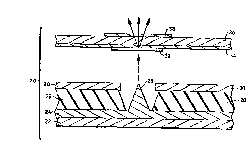
Figure 1 shows an optical printer 10 according to the present invention which isfor l~icordillg electronic images onto a photosensitive recording mP~ m 14. In the
preferred embodiment, the photosensitive recording m~-7illm 14 is an integral film,
lo such as that described in commonly assigned United States Patent No. 4,~63,411
entitled "Copolymeric Mordants and Photographic Products and Processes
ContAinin~ Same" and issued to Irena Y. Bronstein-Bonte on January 7, 1986.
Though this is the preferred embodiment, various other photosensitive recording
media can be substituted without detriment to the invention.
1SThe photosensitive recording medium 14 is fed into the printer 10 by
conveyancing systems well known in the art and is drawn through the printer 10 by
rollers 16 driven by drive motor 18. As the photosensitive recording medium 14 is
pulled through the printer 10, a processor 19 transfers image data to a print head 20.
The print head 20 then projects light (indicated by arrows) onto the photosensitive
20 recording medium 14 such that a coherent image is formed thereon.
The print head 20 is a solid state thin film electron source which generates an
electric field for luminescent excitation of luminophor m~teri~l~ thus producing light. The print head 20 is shown as a line array for im~ging a single line on the
photosensitive recording m~ m 14. An area device lltili7ing a plurality of line
2s arrays can also be used and should be considered an ~ltern~tive embodiment of the
invention.
-
WO96/10835 ~ 2~)~9~7 Pcr/uss5/l2477 ~
The luminophor m~teriAl is one which translates at least a portion of absorbedenergy into emitted lllminescent radiation. In the ~lcfell~d embodiment, the
luminophor is a phosphor based m~tto.ri~l The light is tr~ncmitte-l to the
photosensitive recording m.orlillm 14 by the print head 20. The light then passes
5 through a lens 21. The lens 21 can be a conventional lens or as in the plef~lled
embodiment can be an array of graded index rods, or grinrods. In the case of contact
printin~, the lens 21 would be removed and a light tr~ncmi.ccive faceplate would be
used. Such a faceplate is later herein described.
Figure 2 illustrates a basic construction of a field emission cathode ray tube
lo ("CRT") as applied to the print head 20 of the invention. A cathode tip, or cone 26,
emits electrons as shown by the dashed line which impin~e a face plate 36 coatedwith a luminophor film 34 so as to excite the luminophor film 34 and emit light.The print head 20 is fabricated with an array of the cones 26 deposited on a back
plane 22. These operate at room temperature. Each cone 26 has a sharp radius at its
5 apex such that electron t~lnneling is enabled when a positive voltage is applied to the
gate film.
The back plane 22 is generally a glass substrate upon which the field emission
CRT is f~hric~t.q-l A cathode 24 forms a next layer on the back plane 22 such that
the cathode 24 extends over an entire surface of the back plane 22. The cathode 24
20 has the aforementioned array of cones 26 deposited thereon such that centers of the
cones range in tlict~3n~e from each other from three micrometers to ten micrometers,
and are electric~lly connected at their bases.
The cones 26 are separated from each other by an insulator 28 which is depositedover all surfaces of the cathode 24 which do not have a cone 26 protruding
2s thelc;Loll.. The insulator 28 is fabricated from any of numerous m~teri~lc having a
~ wo 96/10835 2 2 0 0 9 5 ~ PCT/US95/12477
high dielectric strength. In the preferred embo-liment the insulator 28 is silicon
dioxide.
Spaced in a same plane with the apex of the cones 26 is a gate 30 which is
separated from the cathode 24 by the in~ tor 28 and is made of an electrically
conductive metal. The gate 30 is etched with an aperture 40 for each of the cones 26
such that the apex of the cone 26 protrudes through the gate 30.
A positive potential at the gate 30 relative to the cathode 24 produces an intense
electric field at the apex of the cone 26. The field strength is s-lfficie~ to initiate
electron tnnneling from the apex of the cone 26 to a space around the cone 26. Field
strengths of 109 to 101 volts per meter are typical for gate voltages of 80-100 volts
with respect to the cathode 24.
An anode 34 is spaced apart from and above the cones 26 and has a potential
significantly higher than that of the gate 30 such that once electronic tnnn~oling is
initi~te~ electrons are drawn up towards the anode 34 as shown by the dashed line.
A thin film of luminophor 32 is coated on the anode 34 such that as the electrons
impinge upon the luminophor 32, the luminophor 32 is excited and produces a light.
The light can be varied in wavelength dependent upon the choice of luminophor 32and is often one of red, green, or blue depending on a spot color required in the print
head. In this embodiment of the invention, the luminophor film 32 is made of a
broad spectrum phosphor which is used to produce an e~senti~lly white light. Thewhite light is passed through the anode which is tr~ncmi~cive to light and is
tr~n~mitte-l by a face plate 36. Color, in this embodiment, is produced by using a
color filter 38.
Referring now to Figures 3A and 3B, the circuit characteristics of the print head
2s are shown in greater detail. Figure 3A illustrates that as a voltage Vg is placed
across the gate 30 and the cathode 24 through a reci~t~nce Rg, a current .g is produced
W 0~96/10835 ~2 2 0 0 9 5 ~ PCTrUS95/12477 ~
therebetween. Similarly, a voltage Va is placed between the anode 34 and the
cathode 24 through resistance Ra and a current ~,aiS produced. By Kirchhoff's current
law,
+
5 where ~ is current through the cathode 24.
Due to a minim~l attraction of electrons to the gate 30, the resistor Rg is not
actually required. The attraction is minim~l because Vg is small, approxim~t~ly 50
volts, relative to Va which is on the order of 200 volts. In fact, the current i,g is
produced from leakage through the insulator 28 and from stray electrons from theo cathode 24. Therefore, since ~ is minim~l compared to ~a~a can be ignored in the
above equation thus leaving i, - ~a This current flow causes an attraction of electrons
emitted from the cone 26 due to the electron tunneling to be drawn towards the
anode 34 as shown by the dashed lines.
The choice of the gate voltage, Vg, is not albilld y but is instead used to switch
15 sections of cones on and off. If Vg is less than a threshold value, VTH~ tllnn~ling is
not enabled and the electron flow is not created. But as Vg rises, the threshold value
is exceeded and tunneling in the cone 26 causes the ernission of the electrons. This
is graphically seen in Figure 3B where once the threshold voltage, VTH is exceeded
the cathode current increases exponenti~lly with the electron field. This
20 char~cteri~tic allows for easy ~wi~l~ing of individual cones or sections of cones
between on and off, thus multiplexing is enabled. Also indicated on the graph is an
o~ldLillg voltage, VOP~ producing an operating cathode current, 1OP. The opeldti,lg
voltage is chosen to produce sufficient electron flux, to cause sufficient brightness
levels in the phosphor while keeping the cathode current below an amount which
25 will burn out the phosphor.
WO 96/1083~ PCT/US95/12477
~ f~9~1
Groups of these f~eld emitting cones 26 work together to create a single spot for
pnnting purposes. A single spot forrning group is commonly on the order of 104
- cones per square millimeter. This density ensures re(llln~l~ncy and unirull-"ty of
emission.
5Each spot forming group is composed of plural adjacent cones 26 placed
sllfflcie~tly closely together so that outer portions of each electron beam overlap.
This overlap has an additive effect, c~lcing the fields from adjacent cones 26 to form
an electron flux that is relatively uniform. This geometry ensures that multipleparallel beams are efficiently directed substantially along a normal to the anode
loplane and are non-diverging in the dot center region. For example, cones may be
placed appr~ xim~tely five micrometers apart to form an extended array of electron
emiLLel~ which collectively constitute a beam for depositing one charge spot.
Figure 4 shows a print head 20 for multi-color printing that includes mnltirle
arrays of spot forming groups as previously described. In the illustrated
15embodiment, the print head 20 consists of the back plane 22 which carries the gate
30 and the cathode 24 field emission structure. Above that is the face plate 36 with
red, green, and blue luminophor stripes and a common anode 34. The gates are three
electrically independent rows 42 of film which control the red, green, and blue
luminophor stripes. Beneath the gate films running in an orthogonal direction are
20cathodes in columns 42 which are also electrically isolated. The cathodes consist of
field t;llfiLLcl~ which are defined at the intersection of a gate and cathode structure
and are shown in detail in Figure 4. Thus, electron flux is confined exclusively to
the areas at the intersections and are addressable by rectangular coordinates toselectively activate individual areas. The areas define pixels and would be
2sapproximately 100 square micrometers per a 200 dot per inch printer. Each pixel
consists of 600 or more cones 26. The pixels are addressed sequentially one row at a
11
W O96110835 PcTruss5/12477
9 ~ 7 ~
time using pulse width modulation. The gate-to-anode spacing is on the order of 200
to 2000 micrometers providing good proximity focusing of the electrons. This is
accomplished in the preferred embodiment by ~ltili7in~ thin film technology.
The print head can be used as shown for im~gin~ one line at a time or may be runs together with additional single line pAnt head structures to form an area printing
device which conveys an entire image at once.
Figure 5 shows a print head 20 for multi-color printing where like numbers
represent like objects. In this embodiment, time delay multiplexing is utilized to
increase print speeds.
o The print head 20', as before, consists of the back plane 22' which carries the
gate 30' and the cathode 24' field emission structure. Above that is the face plate
36' with red, green, and blue luminophor stripes and a common anode 34'.
The gates are three sets of electrically independent rows of film which control
the red, green, and blue luminophor stripes.
Beneath the gate films running in an orthogonal direction are cathodes in
columns 42 which are also electrically isolated. The cathodes consist of field
emitters which are defined at the intersection of a gate and cathode structure as
previously described. Thus, electron flux is confined exclusively to the areas at the
intersections and are addressable by rectangular coordinates to selectively activate
individual areas.
Unlike the previous embodiment, this embodiment repeats rows of colors such
that there are two rows 50 for im~ging red, two rows 52 for green, and two rows 54
for blue.
A signal sent to the a first row of a single color would then be repeated in the2s second row at a time delayed in accordance with a speed that the photosensitive
recording medium is being moved thereby intensifying the color associated with that
12
~ Wo 9~/10835 2 2 0 a 9 ~ 7 PCTIUS95/12477
row. In this way a faster transport system could be utili7e-1 since a single color need
only be exposed for one half of the exposure time n~cecs~ry for a single row of
- colors. Therefore, the print speed has been a~pruxilllately doubled.
In practice, a photosensitive recording mr~ m is introduced into the optical
s printer where a first row of red is exposed. Since there are two consecutive rows 50
of red the exposure time as colll~a~d to a single row is decreased by one half. The
second row having received the same print data as the first row, only delayed intime, then exposes the same line again for the color red. The photosensitive
recording medium by its nature integrates the two exposures to form one line fully
lo exposed in red. The same process is repeated for the rows of green 52 and blue 54
thus producing a fully exposed line.
As a line is being exposed for green, a next line is being exposed in red to for a
complete image upon the photosensitive recording mr~ lm
The number of rows of color may again be increased to three rows or more each
15 time increasing possible print speed as colllpart;d to the single row embodiment. In
the case of three rows the print speed is increased by a factor of three.
Referring now to Figures 6A and 6B, in order to increase light intensity on the
photosensibve recording medium 14, commonly referred to as the film plane, a fiber
optic face plate is used instead of clear glass for the face plate 36. The fiber optic
20 face plate is particularly useful for direct contact printin~ on low ASA film. Fibers
which have high nl1mrric aperture are used to capture a large fraction of the light
emitted by a top surface of the luminophor 32.
Pixels 46 are defined by spots of luminophor 32 which are deposited on the
faceplate 36 as a thin film m~teri~l secured by a lithographic process. In the
25 prc;felled embodiment, the pixels 46 are offset with respect to each other to increase
sp~ring between the pixels 46 thereby red~cing crosstalk between the pixels 46.
WO 96/1083S ~ PCT/US95/12477
~2 0~r~ 5 7~ --
An optical reflector 48 is then secured over the pixels 46 to prevent light piping.
The optical reflector 48 is commonly a thin film layer of a reflective metal such as
0.25 micrometers of alllminllm which is used in the preferred embo-lim~nt The
optical reflector 48 ensures that the light is directed to the top surface of the
s luminophor and coupled into the fibers. The alllminl~m must be thin enough so that
energetic electrons reach the luminophor, yet it must be of sufficient thiçkne~ so
that it acts as an efficient reflector of light.
The invention may be embodied in other specific forms without departing from
the spirit or e~sential characteristics thereof. The present embo-liment~ are,
0 therefore, to be considered in all respects as illustrative and not restrictive, the scope
of the invention being inclic~te-l by the appended claims rather than by the foregoing
description, and all changes which come within the mP~ning and range of
equivalency of the claims are therefore intended to be embraced therein.