Note : Les descriptions sont présentées dans la langue officielle dans laquelle elles ont été soumises.
CA 02201653 1997-06-27
A NOVEL CIRCUIT FOR POWER FACTOR AND LAMP EFFICIENCY
BACKGROUND OF THE INVENTION
The disclosed invention is generally directed to power
supplies for switching ballasts for gas discharge lamps
such as fluorescent lamps, and more particularly to a power
supply that provides for improved power factor and lamp
efficiency.
Fluorescent lighting systems are utilized for illumi
nation in a wide variety of localized and general area
lighting applications. These include residential, office,
and factory lighting as well as work lights, back lights,
display illumination and emergency lights.
Known fluorescent lighting systems typically~comprise
a fluorescent lamp, an AC to DC power supply, and a
switching ballast responsive to the power supply for
driving the fluorescent lamp. Considerations with
fluorescent lighting systems include the desire for high
power factor whereby the time varying AC current input to
the power supply tracks the time varying AC voltage input
to the power supply, the desire for lamp efficiency wherein
the amount of time the lamp is deionized is kept at a
minimum, and the desire for low crest factor of the lamp
current for maximum lamp life, wherein crest factor is the
ratio of peak lamp current to RMS lamp current.
With known fluorescent light systems that include an
AC to DC power supply and a switching ballast-, low crest
CA 02201653 1997-06-27
2 PD 91416
factor is readily achieved by including a smoothing filter
capacitor on the DC side of the AC to DC power supply which
holds the rectified DC voltage at or near the peak of the
AC input such that the rectified DC voltage has only a
small amount ripple. However, the power factor of such a
system would be poor since the smoothing capacitor is
charged only at the peaks of the input AC voltage is near
or at it, and thus the AC input current flows only for a
short time intervals at relative large amplitudes. In
other words, the AC input current waveform comprises
current spikes if a filter capacitor is utilized to provide
a smooth rectified DC voltage having only a small amount of
ripple. At the other extreme, omission of a smoothing
filter capacitor on the DC side of the AC to DC power
supply results in high power factor, but unacceptably high
crest factor in the lamp current of switching ballasts as
well as reduced efficiency.
SUMMARY OF THE INVENTION
It would therefore be an advantage to provide an
improved gas discharge lamp electronic ballast circuit that
provides for improved power factor, low crest factor, and
high lamp efficiency.
Another advantage would be to provide an improved gas
discharge lamp electronic ballast circuit that provides for
improved power factor, low crest factor, and high lamp
efficiency at relatively low cost and a lower parts count.
The foregoing and other advantages are provided by the
invention in a gas discharge lamp electronic ballast
circuit that includes a gas discharge lamp; a rectifier
circuit responsive to AC power for providing a full wave
rectified sinewave voltage across output terminals of the
rectifier circuit; a transformer having a primary winding
and a secondary winding; a switching circuit for
CA 02201653 1999-04-12
~ 3 PD 91416
repetitively connecting the rectii'ying circuit full wave
rectified sinewave voltage to the primary winding; a
driving circuit responsive to the: secondary winding for
driving the lamp with a sinusoidal voltage having a
predetermined frequency; a current sensing circuit for
sensing an average of peaks of current flowing in the
driving circuit; and a pulse width modulation circuit
responsive to the full wave rectified sinewave voltage and
the current sensing circuit for pulse width modulating the
switching circuit at the predetermined frequency such that
the rectifier circuit provides a current having a flattened
full wave rectified sinewave waveform.
BRIEF DESCRIPTION OF THE DRAWINGS
The advantages and features of: the disclosed invention
will readily be appreciated by persons skilled in the art
from the following detailed de:acription when read in
conjunction with the drawing wherein:
'_'0 FIG. 1 is a schematic diagram of a gas discharge lamp
electronic ballast circuit in accordance with the
invention.
FIG. 2 illustrates waveforms of selected voltages in
the gas discharge lamp electronic ballast circuit of FIG.
1.
FIG. 3 is a schematic diagram of an illustrative
example of a waveshaping network of the gas discharge lamp
electronic ballast circuit of FIG. 1.
DETAILED DESCRIPTION OF THE DISCLOSURE
In the following detailed description and in the
several figures of the drawing, like elements are
identified with like reference numerals.
CA 02201653 1997-06-27
4 PD 91416
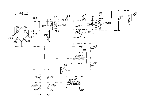
Referring now to FIG. 1, set forth therein is a
schematic diagram of a gas discharge lamp electronic
ballast circuit in accordance with the invention which
includes a full wave rectifier bridge 11 comprised of
diodes lla, llb, llc, lld arranged as a conventional
rectifier circuit wherein the anode of the diode lla is
connected to the anode of the diode llc at a node 101 which
is connected to a ground reference potential, the cathode
of the diode lla is connected to the anode of the diode llb
at a node 102, the cathode of the diode llc is connected to
the anode of the diode lld at a node 103, and the cathode
of the diode llb is connected to the cathode of the diode
lld at a node 104. Standard 60 Hz AC power is connected
across the nodes 102 and 103, and a full wave rectified DC
power output is provided across the nodes 101 and 104. A
relatively small high frequency bypass filter capacitor 13
is connected across the nodes 102 and 104. The high
frequency bypass capacitor is configured to present a
relatively high impedance at 120 Hz and a relatively low
impedance at the switching frequency of pulse width
modulation control circuit discussed further herein. For
the illustrative example of a pulse width modulation
switching frequency of 25 KHz, a bypass capacitance of 0.5
microfarads would provide an impedance of 2500 ohms at 120
Hz and 10 ohms at 25 KHz. In view of the relatively high
impedance of the high frequency bypass capacitor 13 at 120
Hz, the voltage across the nodes 101 and 104 is a full wave
rectified sinewave having a frequency of 120 Hz. There
will of course be a small amount of 25 KHz ripple across
the bypass capacitor 13, but for typical operation this has
no effect and does change the operation.
First and second voltage divider resistors 15, 17 are
serially connected at a node 105 between the node 104 and
the ground reference potential. Third and fourth voltage
divider resistors 19, 21 are serially connected at a node
CA 02201653 1997-06-27
PD 91416
106 between the node 101 and 104. The resistors 15 and 19
are of identical value, and the resistors 17 and 21 are of
identical value. The node 106 is further connected to a
waveshaping network 20 that controls the voltage at the
5 node 106 to be a full wave rectified sinewave having a
flattened top. As discussed further herein, the
waveshaping network 20 can comprise a diode-resistor ladder
that incrementally connects resistive paths to the node 106
as the voltage at the node 106 increases, such that the
voltage waveform at the node 106 is a flattened full wave
rectified sinewave. The voltage at the node 105 follows
the waveform of the full wave rectified sinewave at the
node 104 but at a lower amplitude, and comprises a
reference full wave rectified sinewave that is
representative of the full wave rectified sinewave at the
node 104.
Referring in particular to FIG. 2, schematically
illustrated therein are a waveform V105 of the voltage at
the node 105 and a waveform V106 of the voltage at the node
106 for a one-half of a half sinewave, and for the
illustrative example wherein the rate of increase of the
voltage V106 at the node 106 is decreased in three steps.
During a subinterval X that begins at the start of a half
sinewave, the waveshaping network 20 provides no
attenuation and the voltage V106 at the node 106 follows
the voltage V105 at the node 105. During a subinterval A
that begins at the end of the subinterval X, the
waveshaping network 20 provides a predetermined amount of
attenuation, and the voltage V106 at the node 106 increases
at a slower rate than the rate at which the voltage V105 at
the node 105 increases. During a subinterval B that begins
at the end of the subinterval A, the attenuation provided
by the waveshaping network 20 is increased relative to the
attenuation provided during the subinterval A, and the
voltage V106 at the node 106 increases at a slower rate
CA 02201653 1997-06-27
6 PD 91416
than during the subinterval A. During a subinterval C that
begins at the end of the subinterval B, the attenuation
provided by the waveshaping network 20 is increased
relative to the attenuation provided during the subinterval
B, and the voltage V106 at the node 106 increases at a
slower rate than during the subinterval B. Thus, the
voltage V106 at the node 106 comprises a waveform that
increases at progressively slower rates as the amplitude of
the voltage V105 at the node increases in a sinusoidal
manner.
The node 105 is connected to the non-inverting input
of a differential amplifier 23 having its non-inverting
input connected to the node 105. The output of the
differential amplifier 23 therefore comprises the
difference between the reference full wave rectified
sinewave at the node 105 and the flattened full wave
rectified sinewave at the node 106. In particular, for a
full wave rectified sinewave having a period T, wherein T
is the time interval from the start of a half sinewave to
the start of the next half sinewave, the difference is zero
at the start of a period, increases as the half sinewave
increases in amplitude, reaches a maximum at T/2, and then
decreases as the half sinewave decreases in amplitude.
FIG. 2 illustrates a waveform V23 of the voltage output of
the differential amplifier 23 for one half of a half
sinewave.
The output of the differential amplifier 23 is coupled
to via a resistor 27 to a DC feedback input of a pulse
width modulation (PWM) control circuit 25 that for example
operates at a switching frequency of 25 KHz. By way of
illustrative example, the pulse width modulator control
circuit 25 comprises a Unitrode Corporation UC3524B
integrated circuit. An FET gate control output of the PWM
control circuit 25 is connected to the gate of an N-channel
transistor 29. The source of the N-channel transistor 29
CA 02201653 1997-06-27
7 PD 91416
is connected to the ground reference potential, and the
drain of the N-channel transistor 29 is connected to one
terminal of a primary winding T1A of a transformer T1. The
other terminal of the primary winding T1A of the
transformer T1 is connected to the node 104.
A secondary winding T1B of the transformer is
connected to a matching network that includes an inductor
33, a capacitor 35 and an inductor 37.. One terminal of the
inductor 33 is connected to one terminal of the secondary
winding T1B, and the other terminal of the secondary
winding T1B is connected to the ground reference potential.
The other terminal of the inductor 33 is connected to one
terminal of the capacitor 35 and one terminal of the
inductor 37. The other terminal of the capacitor 35 is
connected to the ground reference potential, while the
other terminal of the inductor 37 is connected to a primary
winding T2A of a transformer T2.
The other terminal of the primary winding T2A of the
transformer T2 is connected to one terminal of a sense
resistor 39 which has its other terminal connected to the
ground reference potential. The non-grounded terminal of
the sense resistor 39 is further connected to the anode of
a diode 41 which has its cathode coupled to the DC feedback
input of the PWM control circuit 25 via a resistor 43. A
resistor 45 and a capacitor 47 are connected in parallel
between the cathode of the diode 41 and the ground
reference potential.
A capacitor 49 and a fluorescent lamp 51 are connected
in parallel across a secondary winding T2A of the
transformer T2. The secondary winding T2A and the
capacitor 49 are tuned to the switching frequency of the
pulse width modulation control circuit 25.
In operation, the voltage across the primary winding
T1A of the transformer comprises a series of pulses having
an amplitude that is modulated by the amplitude of the full
CA 02201653 1997-06-27
g PD 91416
wave rectified sinewave across the nodes 104 and 101. The
width of the voltage pulses is controlled by (a) voltage at
the cathode of the diode 41 which represents the long term
average of the peaks of the lamp current as sensed by the
sense resistor 39, the diode 41, the resistor 45 and the
capacitor 47, as described more fully herein, and (b) the
difference between the reference full wave rectified
sinewave voltage at the node 105 and the full wave
rectified flattened sinewave voltage at the node 106. The
current through the N-channel transistor 29 and the primary
winding T1A comprises a series of spaced apart ramps, each
ramp starting when the N-channel transistor 29 is turned on
and ending when the N-channel transistor 29 is subsequently
turned off, and each ramp having a slope that proportional
to voltage. In other words, during each pulse applied to
the gate of the N-channel transistor- 29, the current
through the N-channel transistor 29 and the primary winding
T1A comprises a ramp having a slope that is determined by
the voltage at the node 104. As described further herein,
the width of the voltage pulses across the primary winding
T1A is modulated such that the envelope of the current
ramp peaks comprises a flattened full wave rectified
sinusoid.
The output of the secondary winding T1B of the
transformer T1 comprises a series of pulses that vary in
amplitude with the input AC voltage waveform and vary in
width as determined by the widths of the current ramps in
the primary winding T1A. The matching network comprised of
the inductor 33, the capacitor 35 and the inductor 3'~
provides across the primary winding T2A of the transformer
winding T2 a near sinusoidal voltage having a frequency
that is equal to the pulse width modulation switching
frequency of 25 KHz. The secondary winding T2B of the
transformer T2, the capacitor 49, and the lamp form a
resonant lamp circuit such that the lamp 51 is driven with
CA 02201653 1997-06-27
g PD 91416
a sinusoidal voltage having a frequency that is equal to
the pulse width modulation switching frequency of 25 KHz.
The K or coupling factor from the primary winding T2A to
the second winding T2B allows the lamp current to have a
good sinusoidal waveform. The voltage across the primary
winding T2A will typically have some distortion due to the
pulses from the matching network comprised of inductor 33,
capacitor 35 and inductor 37, but with a loose coupling
factor such as .9 and good Q factor for the resonant lamp
circuit, the lamp current will have low distortion at 25
KHz and some amount of 120 Hz amplitude modulation from the
flattened current envelope in the secondary winding T1B of
the transformer T1.
- More particularly as to the pulse width modulation of
the voltage pulses applied to the primary winding T1A of
the transformer, the width of the pulses is controlled by
the sum of (a) the voltage at the cathode of the diode 41
which represents the long term average of the peaks of the
lamp current as sensed by the sense resistor 39, the diode
41, the resistor 45 and the capacitor 47, and (b) the
difference between the full wave rectified sinewave voltage
at the node 105 and the full wave rectified flattened
sinewave voltage at the node 106, wherein the sum of the
voltages is represented by the sum of the currents at the
DC feedback input of the PWM control circuit as provided by
the resistors 27 and 43. In particular, pulse width
changes inversely with the current sum provided by the
resistors 27 and 43. Thus, the pulse width of the pulses
provided to the gate of the N-channel transistor 29 is
determined by modulation of a desired long term average
current level, as defined by the value of the resistor 43,
with the output of the differential amplifier 23 which
varies with the amplitude of the full wave rectified
sinewave at the node 104.
CA 02201653 1997-06-27
PD 91416
Considering now the operation of the pulse width
modulation of the N-channel transistor switch 29 for
situation wherein the average of the peaks of. the current
to the lamp resonant circuit (comprised of the secondary
5 winding T2B, the capacitor 49 and the lamp 51) is
substantially constant, the widths of the pulses provided
to the gate of the N-channel transistor 29 therefore
decrease with increasing amplitude of the full wave
rectified sinewave voltage, and the intervals during which
10 the N-channel transistor 29 is conductive decrease with
increasing amplitude of the full wave rectified sinewave.
The slopes of the current ramps through the N-channel
transistor 47 and the primary winding T1A increase with
increasing amplitude of the full wave rectified sinewave
voltage, and in accordance with the invention the
waveshaping network 20 and the resistor 27 are configured
such that the peaks of the current ramps that flow through
the N-channel transistor 29 and the primary winding T1A
follow a flattened full wave rectified sinewave. In other
words, the envelope of the peaks of the current ramps
follows a flattened full wave rectified sinewave. As a
result of the high frequency filtering provided by the
bypass capacitor 13 which presents a relatively low
impedance at the 25 KHz pulse width modulation switching
frequency, the waveform of the current flowing out of the
rectifier bridge 11 comprises a flattened full wave
rectified sinewave having the same frequency of 120 Hz and
the same phase as the full wave rectified sinewave voltage
at the node 104 , with a peak amplitude that is less than
the peak amplitude of the envelope of the peaks of the
current ramps through the N-channel transistor 29 and the
primary winding T1A.
Considering further the effect of variation in the
average of the peaks of the current to the lamp resonant
circuit as represented by the current through the resistor
CA 02201653 1997-06-27
11 PD 91416
43, change in the average of the peaks of the current to
the lamp resonant circuit will change the peak amplitude of
the flattened full wave rectified sinewave current flowing
from the bridge rectifier 11. However, in .view of the
output of the differential amplifier 29, such peak
amplitude will always be less than a full wave rectified
sinewave current that would otherwise flow from the
rectifier bridge 11 if the pulse width of the gate control
output of the pulse width modulation circuit 25 were
constant.
Thus, since the current flowing from the bridge
rectifier 11 comprises a flattened full wave rectified
sinewave that follows the full wave rectified sinewave
voltage at the node 104, the circuit of FIG. 1 achieves an
improved power factor. The peaks of current to the bypass
capacitor 13 are not as great as would otherwise occur if
the capacitor were large enough to hold the voltage to near
the maximum amplitude from one cycle to the next. The
crest factor without shaping of the input current as
described above would be high since the lamp 51 tends to be
a constant voltage device, and the unflattened current
peaks would cause very large current to flow in the lamp.
But with the shaping of the input current as described
above, the flattened current envelope into the matching
network, and the loose coupling to the resonant lamp
circuit, the crest factor is greatly improved with minimum
parts and cost.
Referring now to FIG. 3, set forth therein is a
schematic diagram of a waveshaping network that can be
implemented as the waveshaping network of 20 of FIG. 1.
The waveshaping network of FIG. 3 includes a plurality of
diodes D1 through DN, each having its respective anode
coupled to the node 106 of FIG. 1 via respective resistors
R1 through RN. The cathodes of the diodes D1 through DN
are respectively connected '-o respective voltages V1
CA 02201653 1997-06-27
12 PD 91416
through VN. By way of illustrative example, the resistors
R1 through RN are of identical value. The voltages V1
through VN are of increasing voltages that are less than
the maximum amplitude of the reference full wave rectified
sinewave voltage at the node 105. Thus, for example, the
voltage V1 is the lowest voltage and is greater than the
minimum amplitude of the reference full wave rectified
sinewave voltage at the node 105. , The voltage V2 is
greater than the voltage V1, and so forth to the voltage
VN.
The waveshaping network of FIG. 3 operates as follows
for a cycle or half sinewave of the full wave rectif ied
sinewave on the node 104. As the half sine wave voltage on
the node 104 increases, the diode resistor circuits D1, R1
through DN, RN successively become conductive, and the rate
of increase of the voltage on the node 106 is successively
reduced as the voltage at the node 106 successively reaches
the respective voltages of V1 plus a diode drop, V2 plus a
diode drop, and so forth to VN plus a diode drop. As the
half sinewave at the node 104 decreases, the diode resistor
circuits DN, RN through D1, R1 successively become non-
conductive, and the rate of decrease of the voltage at the
node 106 is successively increased as the voltage at the
node 106 reaches the voltages of VN plus a diode drop, VN-1
plus a diode drop, and so forth to V1 plus a diode drop.
Thus, the foregoing has been a disclosure of a unique
gas discharge lamp electronic ballast circuit that provides
for improved power factor, reduced crest factor, and high
lamp efficiency with a reduced parts count
Although the foregoing has been a description and
illustration of specific embodiments of the invention,
various modifications and changes thereto can be made by
persons skilled in the art without departing from the scope
and spirit of the invention as defined by the following
claims.