Note : Les descriptions sont présentées dans la langue officielle dans laquelle elles ont été soumises.
CA 02202311 1997-04-10
SELF-~IO~ nING LINE INTERFACE CIRCUIT
This application claims the benefit of U. S.
Provisional Application No. 60/017372.
FIELD OF THE lNV~L.l lON
This invention relates to the maintenance and
reliability of telephone service provided to subscribers'
lines (loops) and, more particularly, to the interface
circuits (SLICs) serving such lines.
R~CKGROUND OF THE lNv~:NllON
A telephone line circuit, traditionally located at
the telephone central office, provides a number of
functions for the customer loop it serves. "BORSCHT" iS
the mnemonic frequently used to identify the principal
ones of such functions: battery feed, over-voltage
protection, ringing, supervision of the loop,
coding/decoding, hybrid function, i.e., connection of
two-wire subscriber line to the four-wire network, and
testing.
The growing trend to the concentration of customer
lines remote from the central office requires that BORSCHT
functions be provided by line cards remotely located from
the central office switch - with the result that the
automatic testing equipment of the central office is no
longer locally available to the line circuit.
Accordingly, it would be desirable to provide a line
interface circuit which could accomplish, in a self-
contained manner, many of the testing functions priorly
requiring the local availability of central office
switching equipment. Additionally, it would be
advantageous to reduce the cost and size of the line
interface circuit without sacrificing reliability. In
particular, it would be advantageous to eliminate the need
CA 02202311 1997-04-10
for the line transformers and electromechanical loop
isolation relay that has previously been required to
disconnect the Tip and Ring conductors of the customer
loop from the line circuit so the line circuit could be
tested without being affected by, or affecting, conditions
on the loop.
It has heretofore been recognized that one of the
conventional electromechanical relays, namely, the ringing
relay, whose transfer contacts connect the ring conductor
of the loop either to the line circuit or to the ringing
generator, may be replaced by a transistor switch. US
patent 4,652,701 issued March 24, 1987 to R. J. Cubbison,
Jr. teaches that when the relay is replaced by a
transistor switch it is necessary to provide a feedback
path to prevent the finite resistance of the cutoff
transistor from coupling the ringing signal into the line
circuit and-to compensate for the transistor's finite
forward resistance to prevent longitudinal unbalance.
It has also been appreciated, as for example in US
patent 5,341,416 issued August 23, 1994 to J. C. Gammel,
that the rapid detection of the off-hook condition when
the ringing signal is applied to the loop, i.e., high-
speed ring trip, can be achieved by monitoring the ringing
signal polarity and cutting off the ringing current when
it rises above a certain threshold amplitude during a
particular polarity of the ringing voltage.
It would be advantageous if a line circuit could be
provided which was capable, without need for an
electromechanical loop isolating relay, of determining
whether there are false crosses or grounds on the tip and
ring conductors and of verifying the condition of the line
circuit~s fuses, DC feed and voice frequency terminating
impedances, codec and tip and ring driving amplifiers as
well as the ring trip and loop closure detectors. It
would be advantageous to be able to ascertain the
CA 02202311 1997-04-10
condition of these circuits under different battery supply
voltages.
SUMMARY OF THE lNV~L~ lON
The foregoing and other objects and features of my
invention are realized in an illustrative embodiment of a
four-wire line circuit whose circuit components are
selectively controllable by a microprocessor/DSP to
provide normal BORSCHT functions or to be selectively
tested without need for an electromechanical relay to
isolate the line circuit from the loop conductors. The
conventional line transformer is advantageously replaced
by a loop current feed resistor network and either a high
voltage or a lower voltage battery may be connected to
provide loop current to the resistor network through a
current regulator circuit and battery switch circuit. In
normal operation, an ac feedback path, which includes the
line receive amplifier, increases the terminating
impedance above the DC value of the feed resistors so the
loop termination resistor network may match the
characteristic impedance of the loop at the audio
frequencies employed. A level shifting circuit between
the codec analog output and the input to the line driving
amplifiers establishes a DC level for the signal applied
to the loop so as to preserve the dynamic range of the
codec signal irrespective of which battery is connected to
supply the loop. The line receive amplifier, which is
directly coupled to the resistor network, reports on-hook
and off-hook loop status to the microprocessor/DSP through
a comparator which is biased by whichever battery is
supplying the loop. Different discharge paths for the
Miller capacitor, which shunts the current limiter to
provide a low impedance path for the audio frequency
analog signals transmitted over the loop, are selected by
the microprocessor/DSP depending on whether the ringing or
CA 02202311 1997-04-10
the disconnect forward state is to follow the
disconnection of the battery supplying loop. The Miller
capacltor is rapidly discharged prior to ringing so that
it does not loading the ringing signal but slowly
discharged prior to disconnect forward to avoid
introducing a noise spike on the loop.
In the testing mode, the microprocessor/DSP
selectively applies or denies power to the line driving
and receive amplifiers as well as the level shifting
circuit interposed between the codec analog output and the
input to isolate or include these components in the
circuit. The condition of the feed resistors and
protective fuses and of the loop closure detector is
reported to the microprocessor/DSP over the same terminal
normally used for reporting the on-hook and off-hook
status of the loop.
A number of tests are performed, as follows:
1. a loop back test in which the tip and ring driving
and receive amplifiers and their interface to the codec
are turned off to place them in a high impedance state so
as to isolate the codec's input and output from the tip
and ring conductors of the loop, the microprocessor/DSP
applies a digital tone code to the codec's digital input,
the codec's analog output is connected to its analog input
and the codec's digital output is connected to the
microprocessor/DSP for analysis;
2. a tip side transmission test in which the tip side
driving amplifier and the receiving amplifier are enabled
but the ring side driving amplifier is turned off and
placed in a high impedance state; the microprocessor/DSP
issues a digital tone code to the codec's digital input,
the codec's analog output supplies a test tone to the tip
driving amplifier and the tone's reflection from the
CA 02202311 1997-04-10
resistor network as sensed by the receive amplifier is
applied to the codec's analog input and the codec's
digital output is analyzed by the microprocessor/DSP to
determine if the enabled amplifiers, loop terminating
resistors and coupling capacitors are functional;
3. a ring side transmission test which performs
counterpart functions for the ring side transmission path;
4. a test (which uses part of the loop closure detector
circuitry) to report the state of the DC feed resistors
and fuses with high battery applied;
5. a test of the DC feed resistors and fuses with low
battery applied through the current limiter biased for
linear operation with no loop current (as for on-hook
transmission);
6. a test of the loop closure detector forced on-hook,
the receive amplifier being turned off and the input of
the loop closure detector being connected to a voltage
that is a fraction of normal battery;
7. a test of the loop closure detector forced off-hook,
the receive amplifier being turned off and the input to
the loop closure detector being connected to ground;
8. a test of the ringing generator, performed prior to
applying ringing to the phone, in which the 20 Hz clock is
internally forced to + 5V, the ringing generator is turned
on and its output ramped from VBATl to ground;
9. a ring trip test, which follows the test of the
ringing generator, in which the ringing generator is
turned off, an SCR in the over-voltage protection circuit
is turned on and the loop current is limited by the
CA 022023ll l997-04-l0
current limiter. If NRDET reports ring trip to the
microprocessor/DSP too soon or too late after the ring
trip detector is enabled, the condition indicates that
ringing should not be applied to the loop;
10. a ring trip reset state in which the ring trip filter
capacitor is discharged prior to applying ringing to the
loop; and
11. a noise test in which all amplifiers and the receive
interface are powered down but the battery switch is
turned on and the idle channel noise from the loop that
appears at the analog input of the codec is measured.
BRIEF DESCRIPTION OF THE DRAWING
The foregoing objects and features may be come more
apparent when the ensuing description is read together
with the drawing in which:
Fig. 1 is a block diagram of the illustrative
embodiment of a four-wire line interface circuit providing
BORSCHT functions and self-testing under the control of a
microprocessor/DSP.
Figs. 2A and 2B show details of the receive interface
(RI) circuit intermediate the codec and the loop driving
amplifiers and a portion of the loop closure detector of
Fig. l;
Figs. 3A and 3B show details of the current limiter
(CL) and protection (PROT) circuits of Fig. l; and
Figs. 4A and 4B show details of the fuse and DC feed
resistor detector (FDET) and the loop closure comparator
(CMPl) of Fig. 1 as well as the loop closure detector test
CA 02202311 1997-04-10
(LCT) circuitry.
~,T.'~T ~T. DESCRIPTION
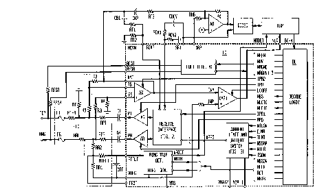
Fig. 1 is a block diagram showing the principal
components of the customer loop interface circuit of the
present invention. At the left-hand side of Fig. 1,
enclosed within the dashed lines, a thick film subassembly
FIC incorporates the DC feed resistors and fuses in one
package having terminals TIP and RNG to which the tip and
ring conductors of the loop circuit are respectively
connected. Subassembly FIC includes fuses FT and FR for
over-current protection of the tip and ring leads,
respectively, and a plurality of resistors for feeding the
DC current or applying the ringing signal to the loop, as
well as for providing basic impedance matching for audio
frequency coupling to the loop. The thick film resistors
of subassembly FIC are advantageously designed to fail
open rather than short-circuited under power cross
conditions and, should a sufficiently heavy power cross
occur to cause the FIC to crack, the opening of the DC
feed resistors would remove battery and ground feed from
the loop.
A second subassembly, IC, contains the major
electronic amplifying and testing components of the line
interface circuit on an integrated circuit chips and an
external codec and microprocessor digital signal processor
DSP complete the arrangement of line interface components
for providing the BORSCHT functions to the loop.
The battery switch of the line interface circuit is
capable of connecting a current limited higher voltage
battery (VBATl) to the loop when the line is on-hook to
increase signaling range and a lower voltage battery
(VBAT2) when the line is off-hook to reduce power
consumption. The line interface subassembly IC includes a
current limiter and battery switch sub-circuit for
CA 02202311 1997-04-10
providing a voltage-regulated, limited current to the loop
from either of the battery supplies as well as for
selecting the battery supply to be used. When the loop is
idling, the battery switch is turned on to employ the
VBATl supply, typically -48V, and regulated current is
applied by the current limiter to the ring conductor at
terminal VREG to provide sufficient open circuit voltage
between tip and ring to allow various customer premises
equipment to work properly at maximum range. When the
subscriber goes off hook, the battery switch is turned off
and the VBAT2 supply, typically -24V, is connected to the
ring lead via the current limiter to minimize power
dissipation. The current limiter provides a maximum of 23
mA current to a maximum loop resistance of 430Q through
480Q of feed resistance. The regulated current is
applied from terminal VREG of the current limiter to the
ring lead via battery feed resistors (typical values) RRl
(75Q), RR2 (125Q), RRF (40Q) and fuse FR. Ground is
supplied to the tip conductor over resistors RT (200Q)
and RTF3 (40Q), and fuse FT. Resistors RFST and RFSR
(each, illustratively 1 megohm) are connected between the
tip and ring leads and the fuse and feed resistance
detector circuit, to be hereinafter described.
Subassembly IC also includes the line driving
amplifiers for the tip and ring of the customer loop AT
and AR respectively and the audio frequency receive
amplifier AX which is directly coupled to the loop
conductors. The audio frequency output signal provided by
amplifier AT at terminal PT is coupled to the tip lead via
capacitor CT and resistors RPT and RTF3, while the audio
frequency output signal provided by amplifier AR at
terminal PR is coupled to the ring lead via capacitor CR
and resistors RPR and RRF. Resistors RPT and RPR are,
typically, 2400Q each. Resistors Rl and R3 directly
couple the tip and ring conductors to input terminals TS
CA 02202311 1997-04-10
and RS of amplifier AX which, at its output terminal XMT,
reports the on-hook and off-hook loop state to input INM
of loop closure comparator CMPl. The ac signal appearing
between tip and ring conductors is sensed by amplifier AX
and applied to the junction of capacitors CBl and CB2.
Capacitor CBl together with resistor divider RTl, RT2
couple a portion of the ac signal to terminal RCVN of the
receive interface RI and capacitor CB2 and resistor RT3
couples the ac signal to amplifier AO at the analog input
of the CODEC, shown at the top right-hand side of Fig. 1.
The current limited DC voltage at the VREG terminal of the
current limiter and battery switch is applied to terminal
INP of loop closure comparator CMPl so that comparator
CMPl monitors the DC state of the loop regardless of the
voltage applied to the loop. Comparator CMPl reports the
loop closure state to the microprocessor/DSP at terminal
NLC.
The various components of subassembly IC operate
under the control of logic level signals delivered by
decode logic DL. Decode logic DL receives logic level
control signals from microprocessor/digital signal
processor DSP over leads BO-B4. In turn, subassembly IC
provides status information to microprocessor/DSP at
output terminals NRDET and NLC. Microprocessor DSP also
sends and receives signals from the codec. Decode logic
DL provides individual control signals to the various
amplifier and testing sub-circuits of subassembly IC
according to the pattern of signals delivered over leads
BO-B4, a detailed list of which appears in Tables 1 and 2.
The integrity of the battery feed resistors and the
fuses as well as the battery potential applied to the loop
is monitored by fuse and DC feed resistor detector FDET
via high resistance resistors RFST and RFSR (each,
illustratively 1 megohm). If one or both of the fuses or
feed resistors fails, the output of the detector will
CA 02202311 1997-04-10
indicate a fault when the loop is on-hook, the output of
the fuse and feed resistor detector being reported to
terminal NLC signal where it is applied to the
microprocessor/ DSP.
When ringing is called for, the battery switch is
turned off and the ringing generator applies ringing
voltage superimposed upon the highly negative battery
supply (typically -180 V) connected at terminal VRS to
terminal VREG. Amplifier AR is placed in the high
impedance state so as not to load the ringing voltage
supplied by the ringing generator. The presence of the
high negative voltage on the ring lead is verified during
ringing by the fuse and DC feed resistor detector circuit
FDET which contains a threshold monitoring circuit that
receives enabling signals NRHVl through NRGHV3 from the
decode logic DL. When the voltage on the ring lead
crosses a predetermined negative threshold, circuit FDET
reports this fact to terminal NLC.
The DC current flowing in the loop during ringing is
monitored by the ring trip detector at terminal RTFLT and
reported to terminal NRDET to indicate to the
microprocessor/DSP when to trip ringing. The phase of the
ringing generator is synchronized to a 20 Hz ringing
clock. If off-hook is reported at terminal NRDET within
25mS from the trailing edge of the 20 Hz clock, ringing
should be tripped with less than one period delay. If
off-hook is detected within 25mS to 50mS from the trailing
edge of the 20 Hz clock, ringing should be turned off
immediately, with no delay. After the ring trip test is
~ 30 concluded, the ring trip reset state is entered and the
external filter capacitor CRT is discharged so that it
will not fault trip the off-hook detector when ringing
signal is applied to the loop. To discharge this
capacitor, the logic circuit supplies the NRTR signal (see
Table I), to turn on an N-channel FET during ring trip
CA 02202311 1997-04-10
reset to provide a short circuit discharge path across
capacitor CRT.
During normal operation of the line interface circuit
the audio frequency signals from the left-hand (analog)
output of the codec are coupled through capacitor CRCV and
resistor RCVl to terminal RCVP of receive interface RI
from which they are applied to differential amplifiers AT
and AR and then capacitively coupled onto the tip and ring
conductors via capacitors CT and CR, respectively. The
voltage across the tip and ring is sensed at terminals TS,
RS by amplifier AX via voltage divider resistors Rl, R3
and R4. The voltage divider resistors apply a fraction,
illustratively one-fifth, of the tip and ring voltage to
amplifier AX. A portion of the output of amplifier AX
appearing at terminal XMT is fed back via capacitor CBl
and resistor divider RTl and RT2 to terminal RCVN to
increase the audio frequency terminating impedance
exhibited to the loop tip and ring conductors. Without
this audio frequency feedback, the terminating impedance
would be determined solely by the DC resistance of
resistors RTF3, RT, and RPT associated with the tip
conductor, and resistors RRF, RR and RPR associated with
the ring conductor. In the illustrative embodiment, this
DC resistance would establish a terminating impedance of
approximately 450Q which is less than the desired loop
terminating impedance of 600 ohms. With the aid of
receive amplifier AX and the feedback path, hereinafter to
be described in connection with Fig. 2B, the terminating
impedance for ac signals is increased to the desired
level.
The signal at terminal XMT is also applied over
capacitor CB2 and resistor RT3 to the inverting input of
codec input amplifier AO. When activated by the channel
test signal HBS from decode logic DL, transistor switch
HBl (Fig. 2A) connects together terminals SBl and SB2 so
CA 02202311 1997-04-10
that the signal at terminal XMT may be summed in resistor
RHB with the signal from the codec analog output. In the
illustrative embodiment, the codec accepts an input analog
signal having a 5 volt dynamic range. To translate this
swing so that it referenced about zero volts, a bias
voltage of 2.5 volts DC is applied to the non-inverting
input of codec amplifier AO so that the signal applied to
the codec would swing between ground and plus 5 volts.
The output of receive amplifier AX is also applied to
the INM input of loop closure comparator CMP1. Resistor
divider RLC1, RLC2 (best shown in Fig. 2A) applies a
fraction of the voltage at terminal VREG to the INP input
of comparator CMP1 so that the threshold for loop closure
detection will be proportional to the voltage at terminal
VREG. Since the loop closure detection threshold varies
with the VREG voltage, the output of comparator CMP1 at
terminal NLC correctly reports loop closure independently
of the battery voltage applied to the loop. In the
normal power-up talk state (see Tables I and II, line 1),
amplifiers AT and AR are powered up, the battery switch is
turned on connecting VBAT1 to the ring lead and terminal
NLC indicates logic high if the loop is open, i.e., on-
hook. When the line goes off-hook (see Tables I and II,
line 2), the battery switch is turned off and VBAT2 is
connected via the current limiter.
During ringing (see Tables I and II, line 3),
amplifiers AT, AR and the receive interface RI are powered
down to conserve power, the battery switch is turned off,
the ringing generator is turned on and the high voltage
detector, Fig. 4B, is enabled. The fuse detector senses
when the ring lead voltage crosses the predetermined
negative threshold and reports a logic level high signal
to terminal NLC to indicate the presence of high ringing
voltage.
CA 02202311 1997-04-10
AC IMPEDANCE MODIFICATION, FIG. 2B
It was mentioned above that the value of the DC feed
resistors would establish a terminating impedance of
approximately 450Q, i.e., less than the desired loop
terminating impedance of 600 ohms for the ac signals
transmitted over the loop. The amount of DC feed
resistance is constrained by the requirement to minimize
off-hook power dissipation while providing a minimum
current, illustratively 23.5 ma., into a maximum loop
resistance of 430 ohms from the lower voltage battery,
VBAT2. This determines that the maximum DC resistance of
the feed resistors cannot exceed about 450 ohms. This is
less than the 600 ohm ac characteristic impedance of the
loop. To make the ac driving point impedance of the line
interface circuit match the 600 ohm characteristic
impedance of the loop, despite the lower DC resistance of
the feed resistors, a feedback path comprising amplifier
AX and the level shifting receive interface RI is
employed.
For purposes of analyzing how the ac feedback path
increases the effective ac impedance looking into the
loop, reference may be made to Fig. 2B where the
differential amplifiers AT and AR have been replaced by a
simplified, composite amplifier G=A and the feedback path
amplifier AX has been replaced by the box
"-k". In Fig. 2B, RL represents the 600 ohm
characteristic impedance of the loop while the total tip
side DC feed resistance (Fig. 1: RT + RTF3 = 240 ohms) and
the total ring side DC feed resistance (Fig 1: RRF + RR2
+RRl = 240 ohms) have been replaced by a single resistor
Rf . When the interface circuit presents a terminating
impedance of 600 ohms to the loop, the combination of Rf
in parallel with the impedance presented by the amplifier
and feedback path must be 600 ohms. The composite
CA 022023ll l997-04-lO
14
amplifier has a gain of A from its inverting input (-) and
a gain ~f ARCVP from its non-inverting input (RCV) .
Let the parallel combination Of RL and Rf be
represented by RL ' . Let us assume a unit driving point
current, I, into point v1 with VRCVN zero:
A R 4700 16 (1)
RT 300
A R 4700 16
RT 300 (2)
A R 4700 16 (3)
RT 300
Dividing equation (3 ) by vO yields the driving point
admittance, 1/RT
A, _ . 3 .16 (4)
which, assuming the 600 ohm line will be terminated in 600
ohms by the line interface circuit, makes RT=300 ohms.
Now, solving equation (4) for kA:
A - - ~ - - 16
RT 300 (5)
CA 02202311 1997-04-10
R 4700
A . _ . - 16 (6)
RT 300
R 4700
R T 300 ( )
A R 4700 16 (8)
RT 300
From equation (4),
R 4700
A - -- - 16
RT 300 (9)
and substituting into (8):
A . _ . _ - 16 ( 10 )
RT 300
Accordingly, for RT = 300 ohms and using a receive
gain ARCV Of 1, R~ = 480, R = 4700 ohms, and RLI = 266
ohms and substitRutin~7~0hese values into equation (5):
A . -- . - 16
RT 300 (11)
and, from equation (10):
R 4700
A - - - 300 -16 (12)
Substituting the value found in equation ( 12 ) into
equation (11) yields k = 3/16 = 0.188. If the gain of the
CA 02202311 1997-04-10
16
AX amplifier is 0.2, then the values of resistors RT1 and
RT2 of Fig. 1 should be in the ratio of 0.188/0.2 or 0.94.
RECEIVE INTERFACE "RI" and LOOP CLOSURE DETECTOR (FIG. 2A)
The receive interface RI receives the "single-ended~'
output of the codec and supplies differential analog
signals to the line driving amplifiers for the tip and
ring, AT and AR, respectively. In addition, the receive
interface establishes the DC level of the analog signal
which the line driving amplifiers apply to the tip and
ring conductors so as to accommodate the maximum dynamic
range of that signal as provided by the codec analog
output. It will be recalled that the tip conductor is
normally at or close to ground potential while the ring
conductor is at a negative voltage. The receive interface
establishes the DC level of the analog output midway
between ground and VBAT1 to prevent clipping of the
codec's analog signal by the potential appearing on the
loop conductors. More particularly, the "single-ended"
analog output of the codec is connected to terminal RCVP
of the receive interface at the base of transistor B15
whose collector emitter path is situated between a right-
hand pair of constant current sources each denominated
IRef both of which are controlled by the IPR1 signal
issuing from decode logic DL. When the IPR1 signal is in
the "0" state, the constant current sources are powered
up. The upper-most source may be thought of as a source
while the lower-most source may be thought of as a
constant current sink of the same current value,
illustratively 200 microamperes. The emitter collector
path of another transistor, B16, is similarly connected
between a corresponding pair of constant current sources.
The base of transistor B16 is connected to the junction of
resistor divider RT1, RT2 at terminal RCVN. Both pairs of
constant current sources are controlled by the IPR1 logic
CA 02202311 1997-04-10
level signal from decode logic DL. If the analog signal
output of the codec applied to the base of transistor B15
would tend to increase the conductivity of this
transistor, the increased emitter current cannot come from
the upper right-hand constant current source but must be
supplied by resistor R12 diverting some of the current
supplied by the upper left-hand constant current source
that would normally flow through transistor B16. But
since the lower left-hand constant current source must
continue to sink the same amount of constant current that
it did before the codec drove the base of transistor B15,
the diverted current must be returned to it. The
increased current through the collector of transistor B15
flows from point ARP through serially-connected resistors
R13 and R14 to point ATP where it returns to the lower
left-hand current sink. The increased current through
resistors R13 and R14 makes point ARP more positive with
respect to point ATP. Accordingly, point ATP in the
collector circuit of transistor B16 is driven 180~ out of
phase with the drive applied to point ARP in the collector
path of transistor B15 so that amplifiers are provided
with the required differential analog signals albeit the
codec only provided a single-ended output. The analog
drive at point ATP is applied to the non-inverting input
of amplifier AT while the drive at point ARP is applied
the non-inverting input of amplifier AR. When the IPRl
signal is in the "1" state, the constant current sources
are powered down and the output of the codec is isolated
from the input to line driving amplifier AT and AR.
Equal value resistors LCl and LC2 at the input of
buffer amplifier Xl establish the DC level of the analog
voltage developed at points ATP and ARP so that it lies
midway between ground and VBATl. This provides a maximum
dynamic range for the analog signal applied to the tip
and ring conductors. Resistor R22 in series with the
CA 022023ll l997-04-lO
18
inverting input of amplifier AT and feedback resistor R23
across amplifier AT establish the gain of amplifier AT
from its non-inverting input to terminal PT at an
illustrative value of 6. Similar considerations apply to
resistors R24 and R25 associated with amplifier AR.
A noise cancellation arrangement is provided by the
transconductance stage gm, capacitor CBN and VREG so that
any ac noise present at point VREG is applied to point ARP
in a manner to cancel out the noise in the analog signal
applied at RCVP. Briefly, however, any noise voltage
appearing at terminal CBN is converted to a current by the
transconductance stage which current produces a voltage at
point ARP of magnitude and polarity sufficient to cancel
the noise voltage from affecting transmission on the tip
and ring conductors. Further details of the noise
cancellation circuit may be found in the co-pending
application of Ian. A. Schorr, serial number 08/ 359,164,
filed on December 19, 1994.
Referring briefly now to Fig. 1 it will be seen that
the line receiving amplifier AX has its input directly
coupled to the tip and ring conductors of the loop. The
output of the AX amplifier is connected to the inverting
input INM of loop closure comparator CMP1, as shown in
greater detail in the upper right-hand side of Fig. 4A.
The non-inverting input INP of comparator CMP1, as shown
in Fig. 2A, is connected to the junction of resistors RLC1
and RLC2 which form a resistor divider to ground from
terminal VREG that supplies the loop with DC current. The
ratio of RLC1 and RLC2 determines the threshold of loop
closure resistance detectible by CMP1. The NLC output of
comparator CMP1 is reported to the microprocessor/DSP.
Comparator CMP1 thus reports the actual condition of the
loop as determined by the DC state reported by line
receive amplifier AX. When amplifier AX is placed in the
high impedance state, the loop closure threshold may be
CA 02202311 1997-04-10
checked by circuit LCT, Fig. 4A. Circuit LCT can force
the INM input of comparator CMPl to ground (decode logic
DL signals NLCTO=0, NLCTC=0) or to a fraction of VBATl
(decode logic signals NLCTO=0, NLCTC=l).
CHANNEL TEST
Channel test is to be carried out when the loop is
on-hook, as determined by microprocessor/DSP monitoring
terminal NLC for the logic high state. Should the loop go
off-hook during the test program, the test program is
aborted. The logic level signals provided by decode logic
DL to the various components of subassembly IC during the
various tests are set forth in Table I appearing at the
end of the specification.
1. LOOPBACK TEST
In this state, the microprocessor/DSP commands decode
logic DL to issue the signals shown in line 7 of Tables I
and II. The "PD" abbreviations in the "Condition/Test"
column of these tables indicate a power down of the loop
driving amplifiers AT and AR, the loop receive amplifier
AX and the receive interface RI, except as otherwise
noted. The output of the AX amplifier is held at ground
and the current limiter is turned off. With the loop
driving amplifiers and receive amplifiers powered down,
the amplifiers are placed in the high impedance state and
the loop is isolated from the analog input and output of
the codec. With the codec thus isolated from the loop,
decode logic DL applies the HBS signal (Fig. 2A) to turn
on transistors HBl to establish a loop back connection.
In the loop back connection, hybrid resistor RHB is
connected between the output of the codec and its input,
which path may be traced from the codec's output to
terminal SBl through either the P-channel or N-channel
transistors HBl to terminal SB2 and resistor RHB to the
CA 02202311 1997-04-10
inverting input of codec amplifier AO. The microprocessor
DSP may then apply a digital tone signal to the digital
side of the codec which the codec converts to the
counterpart analog signal that is applied through
transistor switch HBl to the inverting input of amplifier
AO and returned to the analog input of the codec,
converted by the codec to the counterpart digital signal
and analyzed by the DSP.
2. TRANSMISSION TEST - TIP SIDE ONLY WITHOUT HYBRID
In this state, summarized at line 9 of Tables I and
II, all circuits are powered up ("PU"), except that the
ring lead drive amplifier AR is turned off ("powered
down") by decode logic DL signal RPD = 1. Switch HBl
located between terminals SBl and SB2 (Fig. 2A) is open so
that terminal RCVP is not connected through to hybrid
resistor RHB (decode logic DL output HBSW =0). The codec,
at its digital input, is instructed by DSP to inject a
test tone, illustratively, -10 dBm at 1 kHz, into the
analog receive port RCVP. Amplifier AT being active and
amplifier AR being powered down, the signal is applied
only to the tip lead. The reflection is sensed by
amplifier AX and appears at transmit port XMT from which
it is applied to the inverting input of amplifier AO and
thence to the analog input of the codec. Should the tip
lead be open, the reflection would be about 6 dB below the
test tone. If, however, the tip and ring are properly
terminated by 600 ohm or 900 ohm impedances, the
reflection will be about 11 dB below the tone. If the tip
lead is shorted to ground, the reflection decreases
significantly to about 23 dB below the test tone. If
there is any failure on the tip side of the interface,
such as an inoperable AT amplifier, an open coupling
capacitor CT and/or resistor RPT, no reflection will
appear at the 4-wire port. If the DC feed resistors (RT,
CA 02202311 1997-04-10
RTF3, RRF, or RR) have failed open while all other
resistors within the dashed lines of FIC remain intact,
there will be massive overload at the 4-wire port. Idle
channel noise received by amplifier AX appears at terminal
XMT and is similarly measured.
3. TRANSMISSION TEST - RING SIDE ONLY; High Battery Fuse ;
Test
In this state, summarized at line 8 of Tables I and
II, all circuits are powered up with the exception of
amplifier AT (decode logic DL signal TPD =1). Hybrid
resistor RHB is disconnected from terminal RCVP by opening
switch HB1 (Fig. 2A). A test tone, -lOdBm at 1 kHz, is
injected by the codec at receive port RCVP. The
reflection appears at the transmit port XMT. Should the
ring lead be open, the reflection would be about 6 dB
below the test tone. If, however, the tip and ring are
properly terminated by 600 ohm or 900 ohm impedances, the
reflection will be about 11 dB below the tone. However,
if for some reason, the ring lead is shorted to ground,
the reflection decreases significantly to about 23 dB
below the test tone. If there is any failure on the ring
side of the interface, such as an inoperable AR amplifier,
an open coupling capacitor CR and/or resistor RPR, no
reflection will appear at the 4-wire port. If the DC feed
resistors (RT, RTF3, RRF, or RR) have failed open while
all other resistors within the dashed lines of FIC remain
intact, there will be massive overload at the 4-wire port.
Idle channel noise is similarly measurable at the 4-wire
port.
4. FUSE TEST - HIGH BATTERY
In this state, summarized at line 10 of Tables I and
II, the line driving and receive amplifiers AT, AR, AX and
receive interface ~I are powered down but the battery
CA 02202311 1997-04-10
switch is turned on (decode logic DL signals NHV = 0,
NBSON = 0). The fuse detector circuit FDET (Figs. 4A and
4B) applies to the NLC terminal output of comparator CMPl
a signal that indicates the condition of the feed
resistors and fuses. The tip lead is connected to ground
and the fuse detector threshold for lead RFST is set to -
27 V. The ring lead is connected to VBATl and the fuse
detector threshold for lead RFSR is set to -35 V. The
fuse & feed resistor detector FDET circuit is enabled by
decode logic DL outputs NFEN = 0, NHV = 0. If the fuses
and DC feed resistors are intact, and the tip lead and the
ring lead are at ground and VBATl, respectively, the FDET
circuit will report a pass condition signal as a logic
high at terminal NLC. If one or both fuses, or one or
both feed resistors (i.e., RT and/or RR) fail open, a
logic low will be reported to terminal NLC. It may be
noted that if the loop goes off-hook during the test, the
FDET circuit will indicate a fault, however,
microprocessor/DSP verifies whether this is a fault
condition by changing to the normal power-up state to look
at the loop closure output on lead NLC. If loop closure
is detected (NLC at logic low), the fault indication is
disregarded.
5. FUSE TEST - LOW BATTERY
This state, summarized at line 11 of Tables I and II,
is the same as fuse test - high battery, except that the
battery switch is turned off (decode logic DL signals
NBSON = 1, NHV = 1). Proper operation of the current
limiter when the loop is in the on-hook condition, i.e.,
when no actual loop current is flowing, requires that a
linearizing bias current be supplied to the current mirror
portion of the battery switch and current limiter circuit.
This bias current (illustratively, 12 mA DC.), may
advantageously be obtained from the ringing generator over
CA 02202311 1997-04-10
lead IBSON which receives the ISON signal from the decode
logic DL. The tip lead is connected to ground and its
fuse detector threshold is set to -27 V. The ring lead is
connected to VBAT2 and its fuse detector threshold is set
to -10 V. If the fuses and DC feed resistors are intact,
and the tip lead and the ring lead are at ground and
VBAT2, respectively, the Fuse & Feed Resistor Detector
will be enabled (decode logic DL outputs NFEN, NHV low)
and indicate a pass condition signal which appears as a
logic high on lead NLC. If one or both fuses, or one or
both feed resistors (i.e., RT and/or RR) fail open, lead
NLC will indicate a logic low.
6. LOOP CLOSURE TEST - NLC FORCED ON-HOOK
In this state, summarized at line 12 of Tables I and
II, all circuits and the battery switch are powered up,
except the receive and transmit paths (amplifiers AT, AR,
AX and the receive interface RI) are powered down to
conserve power. The output of amplifier AX at the INM
input to loop closure comparator CMPl is connected to
voltage that is about 1/5 VBATl to test the loop closure
detection. This checks both the input voltage at terminal
LCTH as well as the operation of loop closure comparator
CMPl. If the loop goes off-hook during the test, this
test will still pass even if the battery switch goes into
current limit. The assumption is made in this test that
since the AX amplifier has passed the above transmission
tests, its DC offset voltage is within specification.
Even if the AX amplifier has drifted away from its
specification, the on-hook and off-hook will still
properly be detected since it is highly improbable that
the AX amplifier could pass the transmission test while
causing the loop closure detection to fail.
CA 02202311 1997-04-10
24
7. LOOP CLOSURE TEST - NLC FORCED OFF-HOOK
This test, summarized at line 13 of Tables I and II,
is the same as above, except that the output of amplifier
AX is connected to ground. The loop closure comparator
CMPl should indicate off-hook. If the loop goes off-hook
during the test, the test will not be affected since the
voltage at terminal VREG should not go to 0 volts.
8. RINGING GENERATOR TEST - OUTPUT AT GROUND
This test, summarized at line 14 of Tables I and II,
is performed prior to applying ringing to the phone and in
preparation for the ring trip test. The receive
transmission path (AT, AR and receive interface RI) is
powered down to conserve power. The 20 Hz clock is
internally forced to +5V, the ringing generator is turned
on and its output is ramped from VBATl to ground. The
VREG detector is enabled and its threshold is set to
detect -15V at terminal VREG. Terminal NLC reports a
logic low (indicating test pass) if the voltage at VREG is
more positive than -15V.
9. RING TRIP TEST
In this test, summarized at line 15 of Tables I and
II, the ringing generator is turned off but the SCR in
the protection circuit, Fig. 3A, is forced on (decode
logic DL signal NSCRON =0) thereby connecting terminal
VREG to ground in series with resistor RRl. The current
limiter is turned on and its output is increased to 55mA.
The ring trip detector output NRDET should indicate a ring
trip condition at approximately 100mS after the circuit is
put into this state. If NRDET indica-tes ring trip sooner
than 70mS, or does not indicate ring trip after 130mS, the
ring trip detector test fails, indicating that ringing
should not be applied to the phone. This test should
always follow the ringing generator, output at ground test
CA 02202311 1997-04-10
and should be performed before ringing is applied to the
phone.
10. RING TRIP RESET
This state, summarized at line 16 of Tables I and II,
5 is the same as Talk State - High Battery, except that
terminals RTFLT and VREG are shorted together to discharge
the ring trip filter capacitor CRT. This test should
always follow the Ring Trip Test and should be performed
before applying ringing to the phone.
11. NOISE TEST
In this test, the receive interface RI as well as the
AT and AR amplifiers are powered down, and the battery
switch is turned on. Idle channel noise is measured by
the microprocessor from the digital signal reported to it
by the codec. The results of this test, along with the
noise test results from the above transmission tests can
be used to determine the source of the noise. If this
test is passed while the transmission tests are noisy,
then the receive interface circuit and/or the AT and/or AR
amplifiers are noisy. If this test is noisy, the noise
probably comes from the customer loop. While there is
some possibility that the noise may be caused by the AX
amplifier, experience indicates that failure of devices of
this kind are in the range of a few parts per million.
CURRENT LIMITER, FIGS . 3A and 3B:
The selection of whether battery VBAT1 or VBAT2 is
connected to the loop is made by turning transistor DM1 on
or off. The higher voltage source, VBAT1, is selected by
transistor DM1 being turned on. The decode logic DL
issues the ISON signal to the current limiter and battery
switch, Figs. 1 and 3, which turns on current source, IRef
putting a reference current into point "11". The
CA 02202311 1997-04-lo
reference current drives the base of transistor Q3A,
turning it on and Q3A then turns on Q3B. The IBSON signal
from the ringing generator circuitry provides 10 ,uA
current to the gate of transistor DMl, turning it on.
Transistor DMl in the turned on state applies VBATl to the
anode of diode D2 whose cathode is connected to VBAT2.
Diode D2 becomes reverse biased since VBATl is more
negative than VBAT2. With diode D2 reverse-biased, the
current limiter output terminal VREG is isolated from
battery VBAT2 and transistor DMl provides a current path
from VBATl to terminal VREG. On the other hand, battery
VBAT2 is connected to supply current to terminal VREG by
turning off transistor DMl and allowing diode D2 to become
forward biased. To turn off transistor DMl, the ringing
generator circuitry is controlled by the NBSON signal
issued from decode logic DL to remove the bias current
applied on lead IBSON and also to supply the IBSOFF signal
to turn on transistors Q8 and Q9 and thereby lower the
voltage at the gate of DMl, turning it off. Capacitor
CBS, at the right hand side of Fig. 3A, is a fairly large
capacitor, illustratively 0.1 ,uf, which provides a
smooth transition in switching between VBATl and VBAT2 by
delaying the turnoff of transistor DMl. Capacitor CLIM,
at the top center of Fig. 3A, which is also illustratively
of 0.1 uf, is connected to the reference current source
in series with resistor R9 and charges toward the
potential of VBATl through the collector emitter path of
transistor Q2 and the source drain path of transistor
DMl. Capacitor CLIM, by functioning as a Miller
capacitor, effectively provides 20 ,uf of capacitance from
terminal VREG to ground at transistors Q3A and Q3B,
thereby lowering the ac impedance to ground offered at
terminal VREG.
The current limiting function is provided by
transistors Ql and Q2 functioning as a current mirror with
CA 02202311 1997-04-10
respect to the reference bias current injected at point
"11". The bases of the current mirror transistors Ql and
Q2 are driven by the Darlington-connected transistors Q3A
and Q3B which function as transistor helpers to augment
the reference current injected at point 11 into the base
of transistor Q3A. The emitter size of transistor Ql is
scaled to have a small fraction, illustratively 1/72, of
the current through Q2 while R2, in the emitter path of
Q2, is a small fraction of Rl in the emitter path of Ql.
With current mirror transistors Ql and Q2 operating in
series with transistor DMl, regulated current is supplied
from source VBATl to terminal VREG. On the other hand,
with transistors Ql and Q2 operating and transistor DMl
cutoff, regulated current is supplied from source VBAT2 to
terminal VREG. The limit to the current supplied out of
terminal VREG is determined by the level of reference
current supplied into point "11". The level of reference
current so supplied is determined by decode logic DL
issuing the ISON or N55MA signals. The N55MA signal, as
shown in Table 1, is in the "0" state to provide a higher
value of reference current into point "11" for on-hook
transmission as well as for the transmission tests, fuse
tests and a loop closure detector test and ring trip test.
Resistor R4 between the emitter of the Darlington
transistors and the bases of the current mirror
transistors, together with capacitor Cl, provide feedback
to stabilize the current mirror-helper transistor
arrangement by inserting a dominant pole in the feedback
loop from the base of Ql, through R12 to the base of Q3A
to provide an adequate phase and gain margin.
To turn off the current limiter, the reference
current supply IRef into point "11" is cut off by decode
logic supplying the NILMON high signal (control path to
IRef not shown). With the removal of the reference
current, the Darlington-connected current-regulating
CA 02202311 1997-04-10
transistors Q3A and Q3B would turn off. However,
capacitor CLIM, which has charged over the path previously
mentioned, will continue to supply a reference current to
the base of Darlington-connected transistors Q3A, Q3B for
some time after the reference current into point 11 is cut
off. If the ringing state (see Tables I and II, line 3)
is to follow the on-hook transmission state, it is
desirable to turn off the current limiter rapidly to
discharge capacitor CLIM so that it does not shunt the
ringing generator. To turn off the current limiter
rapidly, decode logic DL makes the ILMR signal high,
turning on the Darlington-connected transistors Q6A and
Q6B to provide a discharge path for capacitor CLIM from
VREG.
If, on the other hand, the disconnect forward state
(see Tables I and II, line 5) is to ensue, it is desirable
to turn off the current limiter softly so as not to send a
noise impulse down the loop. To turn off the current
limiter softly, ILMT is made high to turn on Q25 and Q26.
These transistors then provide a path for the discharge of
the capacitor in series with resistor Rl9 so that
capacitor CLIM can continue to provide a temporary
reference current into the current mirror.
CA 02202311 1997-04-10
29
CURRENT LIMITER REFERENCE SOURCE, FIG. 3B
Fig. 3B includes a current mirror circuit that, under
the control of microprocessor/DSP issuing control signals
to the decode logic DL, provides different reference
currents to point "11" of the current limiter circuit of
Fig. 3A. In addition, the circuitry at the right-hand
side of Fig. 3B provides drive currents to terminals ILMR
and ILMT at the righthand side of Fig. 3A to turn off the
current limiter before ringing is applied to the loop and
incident to disconnect forward, respectively.
Transistor M10 is the principal input transistor and
transistor Mll is the principal output transistor of a
current mirror circuit for providing controlled current to
point "11" shown at the bottom of Fig. 3B and at the
righthand side of Fig. 3A. In the illustrative
embodiment, transistors M10 and Mll are field effect
transistors. Their channel width-to-length ratios are
relatively scaled, illustratively by the factors of (93)
and (240), respectively, so that output transistor Mll
20 Wi11 deliver to point "11" about 2.5 times the input
reference current IREF to transistor M10. (It should be
apparent, however that if bipolar transistors were to be
used, the relative areas of their emitters rather than
channel width-to-length ratio would be the relevant
factor.) Transistor M10 is normally conducting in series
with diode-connected transistor Q20 whose collector, as
well as the base of transistor Q21, are drained by the 90
microampere reference source IREF SO long as the decode
logic DL provides control signal ISON=0. The bases of
transistors Q20 and Q21 are connected together so that
both have the same base to emitter voltage. Because of
the channel width-to-length scaling factors of transistors
M10 and Mll, the output current delivered to point "11" by
transistor Mll is larger than the reference current
CA 022023ll l997-04-lO
supplied into transistor M10. In addition, however, the
output current delivered to point "11" may advantageously
be supplemented by current from one or more of paralleled
transistors M12 through M15, as will hereinafter be
described. For convenience, however, the operation of
the circuit will first be described ignoring transistors
M12 through M15.
The drive current provided to point "11", shown at
the bottom of Fig. 3B and also at the righthand side of
Fig. 3A, by transistor Mll (through transistor Q21) is
varied by switching transistor M21 into or out of parallel
with transistor M10. This varies the channel width-to-
length ratios of output transistor Mll relative to that of
the either the combined input transistors M10 and M21
connected in parallel or to that of input transistor M10
alone.
During the normal high or low battery talk state when
the loop current is to be limited to approximately 23 ma.,
decode logic DL maintains the N55MA=1 signal thereby
keeping transistor M20 off and allowing inverter G2 to
turn on transistor Ml9. Turning on transistor Ml9 turns
on transistor M21 and effectively connects it in parallel
with current mirror transistor M10 thereby lowering the
channel width-to-length ratio between output transistor
Mll and input transistors M10 and M21 in parallel. The
channel width-to-length ratio of transistor M21 is 120
thereby providing an increased ratio above that provided
by transistor M10 alone. When it is desired to increase
the amount of current that the loop can draw, transistor
M21 is switched out of parallel with transistor M10
thereby raising the ratio between output transistor Mll
and input transistor M10. For the on-hook transmission
state, current is limited to 55 ma. by the decoder logic
DL issuing the N55MA = 0 signal. This signal turns on
transistor M20 which turns off transistor M21, removing
CA 02202311 1997-04-10
transistor M21 from being in parallel with current mirror
input transistor M10 and increasing the channel width-to-
length ratio between the input and output transistors of
the current mirror because the current ratio is determined
by the relative size of output transistor Mll and input
transistor M10 alone rather than by the relative size of
output transistor Mll and input transistors M10 and M21 in
parallel.
At the righthand side of Fig. 3B two other switching
circuits are shown in dotted outline boxes. These
switching circuits are similar to the above-described
switching circuit that includes transistors Ml9 through
M20 but, instead of varying the ratio between the emitter
areas of input transistor M10 and output transistor Mll,
provide alternative output transistors M18 and M24. In
the right-most dotted outline box, the gate of output
transistor M18 can be connected to the gate of input
transistor M10 by transistor M16 so that transistor M18
and transistor Q22 in series can function as the output
transistors of a current mirror to terminal ILMR just as
transistors Mll in series with transistor Q21 functioned
as output transistors to point "11". The emitter area
(215) of current mirror output transistor M18 is larger
than the emitter area (93) of current mirror input
transistor M10. During the normal talk state, decode
logic DL issues control signals NILR=0 and NILT=0, thereby
preventing transistors M18 and M24 from turning on because
both transistors M17 and M23 are turned on. Transistor
M23 shunts the gate and source of transistor M24 while
transistor M17 shunts the gate and source of transistor
M18, thereby preventing transistors M24 and M18 from
turning on. With transistor M24 off, there is no current
path for transistor Q24 to terminal ILMT and with
transistor M18 off there is no current path for transistor
Q22 to terminal ILMR. Accordingly, the circuit of Fig. 3B
CA 02202311 1997-04-10
continues to supply a reference current to point "11" to
current limiter circuit of Fig. 3A so that it functions
normally to supply current regulated voltage to terminal
VREG.
On the other hand, when decode logic DL issues the
command NILR=l, which is issued to define the state
preceding the application of ringing to the loop,
transistor M17 is turned off but inverter Gl turns on
transistor M16 which turns on current mirror output
transistor M18, thereby completing a current path through
transistor Q22 to terminal ILMR shown at the righthand
side of both Figs. 3B and 3A. The current to terminal
ILMR turns on transistor Q6A of Fig. 3A which provides a
rapid discharge path for capacitor CLIM, as described
above. It should be noted that transistor M18 is
advantageously made with an effective channel width-to-
length ratio (215) several times larger than that (93) of
transistor M10, illustratively two and a half times
larger, so that transistor M18, when turned on, provides a
larger current drive to terminal ILMR than is provided to
current mirror input transistor M10.
Similarly, when decode logic DL issues the NILT =l
signal, which is the state preceding disconnect forward,
transistor M23 is turned of and transistor M22 is turned
on thereby turning on transistor M24 which completes a
current path to terminal ILMT shown at the righthand side
of Figs. 3B and 3A. Likewise, transistor M24 is
advantageously made with a channel width-to-length ratio
several times larger than the emitter of transistor M10,
illustratively two and a half times larger, so that
transistor M24 when turned on provides a larger current
drive to terminal ILMT than is provided to current mirror
input transistor M10.
It was mentioned above that transistor Mll is part of
the output current half of the current mirror circuit
CA 022023ll l997-04-l0
driving point "11". Actually, the width-to-length ratio
of transistor Mll may be augmented by one or more of the
P-channel transistors M12 through M15. Any of these
transistors may be connected (prior to installing the line
circuit unit), by converting one or more of the array of
zener diodes Z13, Z12, Zll, Z10 (connected between the
drain terminal of each of transistors M10 - M15 and the
emitter of transistor Q21), into a resistor. The
breakdown voltage of the zener diodes (illustratively 14
volts for Vcc of 5 volts) is such that, under normal
circuit conditions, none of them would be conducting.
During manufacture, one or more of the zeners may be
converted into a resistor in a process known as binary-
weighted melt-back, or "Zener zap" adjustment. The
number of zener diodes so converted is determined by the
total output current required to be supplied to point
"11" .
PROTECTION CIRCUIT, PROT, FIG. 3A:
The lower left-hand portion of Fig. 3A shows the
lightning protection circuit whose terminal PROT is
connected to the DC feed resistor network at the junction
of resistors RR2 and RRl. Should some external event
apply an abnormally high negative potential to the loop,
that potential applied to terminal PROT, is conducted
through resistor R2 to cause zener diode array ZlP to
break down, turning on transistor Q2P. When the current
drawn through resistor R2 causes a voltage drop across the
resistor that exceeds about 0.7 volts, SCRl will be turned
on, temporarily grounding the overly negative voltage. On
the other hand, if an external voltage causes terminal
PROT to rise above its normal potential, diode Dl will
become forward biased and ground the over-voltage.
In addition to functioning as an over-voltage
protector for the loop, the protection circuit also
CA 02202311 1997-04-10
34
functions in a test mode to test the ring trip circuit
that is connected to resistor RTFLT, Fig. 1. This test is
performed in response to the decode logic DL issuing the
NSCRON = "0" signal which turns on transistor QlP.
Transistor QlP turned on, in turn, turns on transistor
Q3P. Transistor Q3P turned on, turns on transistor Q2P
which triggers the SCRs. The conducting SCRs draw
sufficient current from the ring generator to simulate an
off-hook condition of the customer loop.
FUSE and FEED RESISTOR TEST CIRCUIT (FDET), FIGS. 4A and
4B:
The DC feed resistor and fuse detector circuit
informs the microprocessor/DSP at terminal NLC as to the
condition of the fuses and DC feed resistors of Fig. 1,
whether VBATl or VBAT2 is being fed to the loop. In
addition, that part of the FDET circuit shown in Fig. 4B
reports to terminal NLC whether high voltage is being
applied to the ring lead during ringing. Terminal NLC
will remain high during test to indicate the components
are intact. The condition of the feed resistors and fuses
is ascertained through resistors RFST and RFSR which have
a fairly high value, illustratively, one megohm.
To test the DC feed resistors and fuses when VBAT2 is
feeding the loop, decode logic DL issues the NFEN = "0"
and NHV="l" signals. The NFEN =0 signal turns on
transistor B15a while the NHV=l signal turns off
transistor B17. Current drive is provided at terminal
VPR3 to the bases of transistors B12 and B14. Transistor
B15a, when turned on, provides an emitter current,
illustratively 20 ~A, through resistor RlE to transistor
B12 and an emitter current, illustratively 10,uA, through
resistor R7B to transistor B14.
To test the DC feed resistors and fuses when VBATl is
feeding the loop, decode logic DL issues the NHV = "0"
CA 02202311 1997-04-10
signal, turning on transistor B17 making available to
transistor B14 through resistor R7A, an additional emitter
current, illustratively 20 ,uA, thereby supplying
transistor B14 with a total of 30 ,uA. The different
current supplies made available to transistors B23 and B24
make these transistors sensitive to different threshold
conditions at terminals RFSR and RFST to permit testing of
the DC feed resistors and fuses of Fig. 1 whether VBAT1 or
VBAT2 is supplying current to terminal VREG and, in fact,
to verify whether the expected battery supply is in fact
connected.
When so enabled by the NFEN and/or NHV signals from
decode logic DL, transistors B12 and B14 make available
different value reference currents to the collectors of
transistors B23 and B24 whose emitter circuits are
connected, respectively, to terminals VBAT1 and RFSR.
When VBAT1 feeds the ring lead and when the fuse RF and DC
feed resistors of Fig. 1 are intact, transistor B24 should
draw approximately 40 microamperes causing its collector,
and the base of the left OR gate transistor B5, to go low.
The OR gate transistors B5 supply drive to the base of
transistor BlY whose collector is connected to terminal
NLC. When the left OR gate transistor B5 is off, terminal
NLC remains high. If, for any reason, one of the
aforementioned Fig. 1 DC feed resistors or fuse FR is
open-circuited, transistor B24 will not conduct any of the
current made available by transistor B14. The collector
of transistor B24 will therefore be at a logic high,
turning on the left OR gate transistors B5 which, in turn,
turns on transistor BlY causing its collector, which is
connected to terminal NLC, to go low. Referring to Fig.
1, it is seen that the low signal at terminal NLC is
reported to the microprocessor/DSP as a trouble condition
occurring during the feed resistor and fuse test.
CA 02202311 1997-04-10
36
With respect to terminal RFST, the normal ground
potential which should be reflected there from the tip
lead of Fig. 1 will cause current mirror transistor B33
to turn on, turning on transistor B34 and causing
transistor B23 to draw the current made available through
transistor B23. Current through transistor B23 causes its
collector to go low, turning off transistor B22 and
removing the base drive for the right-hand one of OR gate
transistors B5. If neither of the B5 transistors is
turned on, transistor BlY will not be turned on, and
terminal NLC will remain high informing the
microprocessor/DSP that the fuses and DC feed resistors of
Fig.l are operating correctly. Accordingly, it is seen
that for a logic high to be reported to terminal NLC,
transistor BlY should not be turned on and this will be
the case so long as both transistors B23 and B24 are
conducting and their current exceeds the current through
transistors B12 and B14. It will be appreciated that when
the decode logic issues the NHV = "0" signal the threshold
of the feed resistor and fuse detector circuit is set to
indicate the condition of the feed resistors and fuses
where VBATl is feeding the ring lead. If, however, VBATl
is not so connected, the current through transistor B24
will not exceed the current through transistor B14 and the
high signal at the collector of transistor B24 will turn
on the OR gate B5 and terminal NLC will report a low to
the microprocessor/DSP. Accordingly, the feed resistor
and fuse detector circuit functions to test that the
expected battery VBATl is in fact connected when expected.
Transistors B10 and B27 provide clamping to prevent
saturation of the collectors of transistors B12, B14, B23
or B24 under the different working potentials that may be
reflected at terminals RFSR and RFST in practice.
CA 02202311 1997-04-10
LOOP CLOSURE TEST CIRCUIT (LCT), FIG. 4A:
Two tests of the loop detector are performed, first
with terminal NLC forced on-hook and then with terminal
NLC forced off-hook. For both tests the current supply to
the AX amplifier (IPR2 = 1) is removed, thereby placing
the output of the AX amplifier, which is connected to
terminal INM of comparator CMPl, in the high impedance
state.
For the forced on-hook test, a voltage 1/5 of VBATl
is applied to terminal INM by the LCT circuitry shown in
the lower right-hand portion of Fig. 4. This potential is
obtained from the tap of resistor divider Rx, Ry which is
connected between VBATl and ground. The tap of divider
Rx, Ry is connected to the base of transistor B3F. At
this time, as shown in line 12 of Tables I and II, decode
logic DL issues the NLCTO = 0, NLCTC = 1 signals, the
former turning on transistor BlB and the latter turning
transistor B5Y off. Transistor BlB provides a current for
transistors B3E, diode Y2 and current mirror transistors
B35F and B2Y2. (In this path, base bias current for
transistor B3E is provided by the same base rail VPR3 as
supplied the base of transistor B12 of the FDET circuit,
described above.) The current into transistor B35F is
reflected as a current in current mirror transistor B2Y2.
The current through transistor B2Y2 pulls down a current
through diode Y3 and emitter-follower BlY. The emitter
follower clamps the potential at terminal INM to
approximate the same voltage that is presented at the tap
of divider Rx, Ry which may be appreciated by observing
that the path from the tap to terminal INM passes through
four conducting diode drops, two involving potential rises
and two involving potential drops. Since the potential at
the tap of divider Rx, Ry is approximately 12 v DC, that
is the potential to which terminal INM is clamped. It
will be recalled from the description of the loop closure
CA 022023ll l997-04-lO
38
detector that the other terminal of comparator CMP1,
terminal INP, Fig. 2A, is connected to the tap of resistor
divider RLC1, RLC2 to vary the loop closure detector
threshold in accordance with the actual voltage present at
terminal VREG. It will be recalled that amplifier AX, in
normal operation, applies to terminal INM the actual on-
hook and off-hook potentials existing between the loop
conductors and this potential may vary significantly.
Accordingly, when amplifier AX is in normal operation and
circuit LCT is not activated to check the operation of
the loop detector, circuit LCT must present a high
impedance to terminal INM.
For the forced off-hook test of the loop detector,
described at line 13 of Tables I and II, conditions are
the same except that the logic detector DL issues signals
to circuit LCT so that terminal INM of comparator CMP1 is
forced to ground. The NLCTC = 0, ISON = 1 and N55MA = 0
signals from decode logic DL turn off the normal reference
current drive to the current limiter and, instead, provide
a reference current drive that will limit the loop current
to 55 mA. The NLCTC = 0 signal turns on transistor B5Y at
the upper right-hand corner of the LCT circuit. Turning
on transistor B5Y applies Vcc to the emitter of transistor
B4F causing it to conduct heavily. This produces
sufficient voltage across the base biasing resistor for
transistor BlY to draw the base of transistor BlY upward
to ground. This forces terminal INM to ground.
HIGH VOLTAGE DETECTION, FIG. 4B:
During ringing, the high negative battery applied at
30 terminal VRS (Fig. 1) is applied to the ring lead through
the ringing generator. The fuse and DC feed resistor
detector circuit FDET is enabled by decode logic DL
signals NRHV1 through NRGHV3 low, while signal LCOFF high
(Fig. 4A), turns off transistor B5 in loop closure
CA 02202311 1997-04-10
39
comparator CMP1 thereby preventing the loop closure state
from affecting terminal NLC. Resistor R4, Fig. 4A, thus
keeps terminal NLC high unless it is dragged down by
transistor BlY2, Fig. 4B. When the circuit is not in the
5 ringing test states (terminals NRGHV1 through NRGHV3 all
high), transistors BX2L, resistor R2E and transistor B4Y1
disable transistor BlY2 so that it does not falsely drag
down terminal NLC. Separate drives are provided by decode
logic DL to transistors BXlL to accommodate both the
10 ringing generator at ground test and the ringing generator
high voltage test. During the ringing generator at ground
test, terminal NRGND is placed in the logic low state by
decode logic DL while during the ringing generator high
voltage test, terminals NRGND and NRGHV1 are both low.
15 Terminal VREG, Figs. 1 and 4B, is connected to the emitter
of transistor B2EX, Fig. 4B, through series-connected
resistors RLC1 and RLC2. The emitter of transistor B2EX
and terminal IREG are kept at ground by transistors B32F,
B3lF, B19F and the drive at terminal VCL. Transistor B19F
20 supplies current to bias transistors B31F and B32F which
set up a reference voltage for transistor B2EX. With
transistor B32F conducting, its emitter is at ground
thereby placing the base of transistor B2EX at ground.
The collector current of transistor B2EX is provided by
25 the enabled transistors B18F, the series combination of
transistors B30F and BXlLB and the series combination of
transistors B29F and B5Y.
In the illustrative embodiment the combined
resistance of resistors RLC1 and RLC2 is 0.6 megohms so
30 that when terminal VREG is at -130V and the emitter of
transistor B2EX is at ground the current through
transistor B2EX will be approximately 215 ,uA. When the
potential at terminal VREG is closer to ground than
-130V, there will be less than 215 ,uA through transistor
35 B2EX and the potential at its collector (point "52") will
CA 02202311 1997-04-10
be high enough to keep the Darlington connected
transistors B3Y2 and B4Y2 on. When the Darlington
transistors are on they turn transistor BlY2 on.
Transistor BlY2 in the on state keeps terminal NLC dragged
down to a logic low level. When the potential at terminal
VREG goes through the -130V threshold in the negative
direction, the Darlington transistors and transistor BlY2
are turned off, allowing terminal NLC to reflect a high to
the microprocessor/DSP.
It will be recalled that, in the non-ringing
generator test states, the loop closure comparator CMP1
functions as a loop resistance detector since the
threshold for loop closure detection is varied in
accordance with the voltage at VREG. When the absolute
value of VREG drops too low for accurate loop state
detection, there will not be enough current for the loop
to operate and terminal NLC should report the on-hook
condition to the microprocessor/DSP. Accordingly, when
VREG is too small to draw enough current to keep the
Darlington transistors B3Y2, Fig. 4B, off, transistor
B18F, supplies a current to terminal IREG to turn on
transistor B2Y3. The collector of transistor B2Y3 is
connected to terminal NLCOFF which is connected to diode-
connected transistor B3 of comparator CMP1, Fig. 4A.
Transistors B3 and B4 of the comparator form a current
mirror. When transistor B2Y3 draws current from terminal
NLCOFF through transistor B3, a similar current will be
drawn through transistor B4, or transistor B4 will go into
saturation. When transistor B4 saturates, transistor B5
cannot be turned on so resistor R4 forces terminal NLC
high.
What has been described is a line interface circuit
which is configured to permit an assortment of tests to be
performed in a self-contained manner at a location remote
from the central office without the use of an
CA 022023ll l997-04-lO
41
electromechanical relay to isolate the line interface
circuit from the loop. It will be readily apparent to
those having ordinarily skill in the art that numerous
modifications may be made thereto without departing from
the spirit and scope of the subject invention as defined
by the appended claims.