Note : Les descriptions sont présentées dans la langue officielle dans laquelle elles ont été soumises.
f CA 022030~0 1997-04-18
,.
-1-
SOLID STATE AC SWITCH WITH SELF-SYNCHRONIZING MEANS
FOR STEALING OPERATING POWER
BACKGROUND OF THE I~VE~NTION
The present invention relates generally to solid state switching apparatus for
controlling the supply of alternating electric current to a load, and more particularly to a
method and a~ lus for diverting from the supplied alternating current in a self-synchronizing manner the power required for operation of the switching apparatus.
With advances in solid state power switching technology, it has become
0 increasingly common to replace mechanical power control switches with the solid state
switches to achieve long life, quiet operation, and other advantages. However, solid
state switches and the associated control circuitry require electric power for operation,
which is a disadvantage in certain applications. For example, an important application
for the present invention is in replacement of a conventional thermostat having a bi-
metal sensor. In conventional bi-metal thermostats, it has not been necessary to provide
external operating power for achieving on-off action of the switch. In replacing such a
control with one l~tili~in~ solid state power switching components, it is
disadvantageous, and may be difficult to wire in additional power required for circuit
operation. There are also obvious disadvantages to employing a battery for providing
the operating power. A solution which has become p.efelled is to "steal" the necessary
operating power from the power which is being switched.
One of the solid state switching components which is most adaptable for
altern~ting current applications is a power field effect transistor (FET) This component
requires very little power for performing its control function. While single FET's are
available which can switch alternating current, they typically have been expensive or
have marginal capability to provide reasonably high blocking voltages in the off-state
and low impedance in the on-state. These disadvantages can be overcome by employing
two unidirectional low cost power FET's connected in a series back-to-back
configuration. In this manner, good voltage blocking capability is provided for both
polarities of supplied ~lt~rn~ting current, one providing blocking during half cycles of
one polarity and the other providing blocking during half cycles of the opposite polarity.
CA 022030~0 1997-04-18
During periods in which the switching device is in a high impedance "open
switch" state, it is relatively easy to steal the required operating power, since there is
ample voltage across the device. However, during periods in which the device is in a
low impedance "closed switch" state, essentially no voltage is available across the
5 device, and stealing operating power becomes much more difficult.
One known approach to stealing power during periods in which the switching
device is in a low impedance state involves the use of an in-line current transformer.
Such an approach requires provisions for implementing two separate power stealing
techniques, one for intervals during which the switching device is in its high impedance
10 state, and another for intervals during which it is in its low impedance state.
Another approach involves controlling the switching device to its high
impedance state for short intervals during periods that the load is otherwise to be
powered, and diverting power during such short intervals to a storage capacitor. Where
the power is supplied in the form of altern~ting current, it is preferable to synchronize
15 the short power diversion intervals with the ~lt~ ting current waveform.
Synchronization may be accomplished by means of ~;h~;uiLLy including a zero crossing
detector. However, zero crossing detectors typically require sensitive analog
components which both add expense to the control circuit, and require space which may
not be available.
~o The applicants have devised a method and apparatus for accomplishing power
stealing from conductors carrying alternating current both when a switching device
between the conductors is in conducting and non-conducting states in a manner which is
self-synchronized with the alternating current, thereby avoiding the disadvantages of
prior power stealing techniques. Self-synchronized power stealing according to the
2s applicants' method may be readily accomplished with apparatus which is simple,
involves minimum circuitry and is inexpensive to implement.
SIIMMARY OF THE INVENTION
The present invention is a method and apparatus for controlling the supply of
30 alternating current to a load by means of a solid state switching circuit incorporating
cil~;uiLly for stealing operating power from the switched current in a manner which is
' ~ CA 022030~0 1997-04-18
self-synchronized with alternation of the current. During periods in which powering of
the load is commanded, the switching circuit is controlled to its high impedance state for
brief power stealing intervals, successive intervals occurring during separate equally
spaced half cycles of alternating polarity of the alternating current. If the magnitude of
s the diverted current is less than a predetermined threshold, a succeeding power stealing
interval is shifted in time toward the current peak of its associated supply current half
cycle. If the magnitude of the diverted current exceeds the threshold, a succeeding
power stealing interval is shifted in time away from the current peak of its associated
supply current half cycle. The arnounts by which power stealing intervals are shifted in
0 time are preferably unequal for diverted current magnitudes of less than and greater than
the predetermined threshold, one being twice the duration of the other, whereby
balanced power stealing from opposite phases of the supplied alt~ ting current can be
achieved.
The diverted current is used to charge a power storage device which supplies
operating power for the circuit. A current limiter may be provided to limit the current
furnished to the power storage device during periods in which no power to the load is
cornrnanded.
BRIEF DESCRIPTION OF THE DRAWINGS
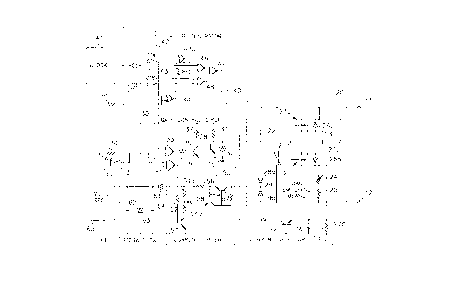
~0 Figure 1 is a schematic diagram of a ~ d circuit for implementin~ the
applicants' invention; and
Figure 2 is a representation of operating waveforrns which occur at selected
points in the circuit of Figure 1, illustrating the manner in which power stealing
intervals are shifted in response to magnitude of the diverted current.
DESCRIPTION OF THE INVENTION
In the schematic diagram of Figure 1, reference numerals 11 and 12 identify a
pair of terminals to which an alternating current electrical load (not shown) may be
connected for control in response to a load control signal provided by an input device
generally identified by reference numeral 13. Input device 13 is schem~tically
represented as including a switch 14, of which the pole is connected to a source of
reference potential or ground 15. In a representative application, and for convenience in
CA 022030~0 1997-04-18
describing the applicants' invention, input device 13 may be considered a thermostat in
which switch 14 is responsive to the difference between a setpoint temperature provided
by an operator and a measured temperature in a space whose temperature is to be
controlled. In such an application the load connected between terminals 11 and 1 7
5 might be the winding of a cooling relay connected in series with the secondary winding
of a 120/24 volt transformer.
Switch 14 is open when there is no ~lem~ncl for cooling in the space. Upon a call
for cooling, switch 14 closes to provide a corresponding control signal to a solid state
load switch generally identified by reference numeral 20. The control signal is
0 produced by a gate control circuit 30 connected between input device 13 and load
switch 20. Gate control circuit 30 also receives a train of pulses from a pulse generator
40, which the gate control circuit logically combines with the load control signal from
input device 13 to produce the control signal for load switch 20.
Gate control circuit 30 and pulse generator 40, as well as certain other functional
15 components require electrical power at a specified voltage, typically five volts DC, for
operation. In addition, as discussed hereinafter, gate control circuit 30 requires a supply
of typically 12 volts DC to produce the control signal required for proper operation of
the power switching elements pl~felled for use in load switch 20. Operating power at
these voltages is diverted from the switched current at power terminals 11 and 1 2, and
~o supplied through a current limiter 50 to a storage circuit 60 which supplies the higher
operating voltage required by gate control circuit 30. Storage circuit 60 also serves as
the supply for a voltage regulator 61, preferably implemented as a switching power
supply circuit, which furnishes the required lower operating voltage.
For several reasons it is important to minimi7~ the power diverted from the
~5 switched current to the control circuitry. One reason is that any power diverted from the
switched current increases the effective voltage drop across load switch 20 when the
load switch is in its low impedance state, and increases effective bleed current (leakage)
when the load switch is in its high impedance state. The less the diverted power, the
greater the range of load ~;ulle~ which can be effectively switched without affecting
30 operation of the controlled load. Conversely, power diverted to operation of the control
circuit is dissipated in the form of heat. This contributes to an offset temperature error
- CA 022030~0 1997-04-18
-5--
which is particularly disadvantageous in thermostat applications. Minimi7ing the power
diverted to control circuit operation minimi7-?s heat dissipation requirements, thereby
permitting a control package of minimum size.
The present invention advantageously employs a current detector 70 in
5 combination with pulse generator 40 to ensure that during periods in which power to the
load is comm~nded, the stolen power is m~int:~ined at a consistent predetermined level.
As will be described hereinafter, this combination generates a train of pulses used to
produce corresponding short power stealing intervals, the timing of individual pulses
and power stealing intervals relative to the supply current waveform being varied to
lO provide for diversion of just sufficient power to permit proper operation of the control
clrcultry.
Turning to the specifics of a ~l~r~ d implementation of the present invention,
load switch 20 is illustrated as including a pair of ideally identical N-channel power
FET's 21a and 21b connected in a back-to-back configuration between power terminals
11 and 12. FET' s 21 a and 21 b either permit or block current flow between power
terminals l l and 12 in response to a control signal on a control signal conductor 22. In
this connection, it should be noted that although field effect transistors in general
consume very little operating power, currently available low cost power FET's require a
control voltage of at least nine volts, and preferably 12 volts, to achieve a solid low
20 impedance "on" state.
Each of FET's 21a and 21b has source and drain power electrodes and a gate
electrode, the source electrodes being connected together at a junction 23 and the gate
electrodes being connected to conductor 22. The drain electrodes of FET's 21a and 2 lb
are connected to power t~rmin~l.s 11 and 12, respectively. The connection between the
25 drain electrode of FET 21b and power terminal 12 includes an over-current protection
feature in the form of series connected resistive elements 24 and 25. Resistive element
24 is a very high temperature coefficient resistor known as a PolySwitch~9,
commercially available from Raychem Corp. Resistive elements 24 and 25 act to
protect FET' s 21 a and 21 b in the event of excessive current through the FET's, which,
30 for example, may result from a field installation wiring error. Resistive element 25
limits the peak current to a value that the FET' s can tolerate for a few seconds, by which
' CA 022030F70 1997-04-18
time the resistance of resistive element 24 has increased thl~ough self-heating so as to
decrease the current to a value the FET's can tolerate indefinitely.
Reference numerals 26a and 26b identify body diodes between the source and
drain electrodes of FET's 21a and 21b, respectively. The body diodes are oppositely
poled, with their anodes at the source electrodes which are connected together at
junction ~-3. Transient protection is provided by a capacitor 27a shown connected
between the drain electrodes of FET's 21a and 21b, and a metal oxide varistor shown
connected between power t~rmin~l~ 11 and 12.
In a typical heating and cooling system application the current source for
powering a load connected to power termin~l.s 11 and 12 supplies altt?rn~ting current at
60 cycles per second and a nominal voltage of 24 volts. This is converted to direct
current for operating the control circuitry by means of a full wave rectifier bridge
comprising body diodes 26a and 26b and an additional pair of diodes 28a and 28b. The
anodes of diodes 28a and 28b are connected to power terminals 11 and 12, respectively.
s The cathodes of 28a and 28b diodes are connected together at a junction 29, at which
unidirectional current is provided. The return for the DC operating supply circuit is
provided by connecting junction 23 to ground l S through current detector circuit 70.
In operation, control signal conductor 22 is biased to a voltage suitable for
m~int~ining FET's 21a and 21b in a low impedance state by means of voltage provided
)o by storage circuit 60 through a bias resistor 31. A zener diode 32 is connected between
conductor 22 and ground 15 to limit the m~imllm voltage applied to the gates of FET's
21a and 21b. FET's 21a and 21b are switched to a high impedance state, as will be
described hereinafter, by overcoming the bias voltage on conductor 22 when switch 14
is open or when a pulse is received from pulse generator 40.
2s The signals from switch 14 and pulse generator 40 are combined by means of a
NOR logic element 33. A first input to logic element 33 is biased to a "high" state by
means of voltage supplied by voltage regulator 61 through a resistor 34. Closure of
switch 14, corresponding to a command for power to the load results in ch~nging of that
input signal to a "low" state. With switch 14 open, logic element 33 provides a "low"
output which is supplied through a resistor 35 to the base of an NPN transistor 36 whose
collector is supplied with the output voltage of storage circuit 60 through a resistor 37,
CA 022030~0 1997-04-18
and whose emitter is connected to ground 15. A "low" output from logic element 33
renders transistor 36 non-conductive. The voltage at the collector of transistor 36 is
supplied to the base of an NPN transistor 38 whose collector is supplied with the output
voltage of storage circuit 60 through resistor 31, and whose emitter is connected to
ground 15. With transistor 36 in a non-conductive state, transistor 38 remains
conductive by virtue of the voltage supplied to its base through resistor 37. This
reduces the voltage on control signal conductor 22 which renders FET's 21a and 21b
non-conductive.
Conversely, a closed state of switch 14 in the absence of a pulse from pulse
o generator 40 results in a "high" output from logic element 33, conduction of transistor
36 and non-conduction of transistor 3 8. This biases the gates of FET's 21 a and 2 lb to a
voltage which m~int~in~ the FET's in a low impedance state, and results powering of
the load connected to power termin~l~ 11 and 12.
When switch 14 is open, pulses from pulse generator 40 have no effect on the
output of logic element 33, and hence, no effect on the voltage on control signal
conductor 22. However, when switch 14 is closed, corresponding to a command for
power to the load and requiring a low impedance state of FET's 21 a and 2 lb, pulses
supplied by pulse generator 40 result in corresponding power stealing intervals during
which FET's 21a and 21b are switched to their high impedance states. Figure 2A
20 illustrates the load current waveforrn with a power stealing interval each half cycle of
the supplied current.
Pulse generator 40 is connected to receive a clock signal from a clock circuit 41.
For a supply current frequency of 60 cycle per second, a lkHz clock pulse repetition
rate would be ideal. This ideal can be satisfactorily appro~im~te~l in a simple low cost
25 manner with a standard time keeping clock circuit implemented with a 32.768 kHz
crystal oscillator and divider which can readily produce a clock pulse repetition rate of
1.024 kHz. For convenience, the following description will assume and be based on an
ideal lkHz clock signal.
The clock signal is supplied to the CLK pin of a decade counter 42 which
~o sequentially produces output pulses of one millisecond duration at output pins CT0
through CT9. Decade counter 42 also has a reset pin which requires a ~'low" signal for
CA 022030~0 1997-04-18
continued operation of the counter. Interruption of the "low" signal termin~tes the
counting sequence, and causes pulse generation to start over at pin CT0.
The pulses produced at selected output pins are used for various purposes.
Specifically, pulses at pin CT4 are used to reset a flip flop comprising cross-coupled
NOR logic elements 43a and 43b prior to generation of a power stealing pulse. Pulses
at pin CTS are used to enable a power stealing pulse and a current sampling interval for
current detector 70. Pulses at pins CT8 or CT9 are used to reset the operation of counter
42 based on the state of certain additional logic in pulse generator 40 which causes reset
of counter 42 after a pulse at pin CT8 or CT9 based on the status of flip-flop 43a, 43b.
0 Pulses at pin CT4 of counter 42 are supplied to one input of logic element 43a
which serves as a reset input of flip flop 43a, 43b. The set input of flip flop 43a, 43b
formed by one input terminal of logic element 43b is connected to the output of a NOR
logic element 44 connected as an inverter. Both inputs of logic element 44 are biased
"high" by voltage provided from voltage regulator 61 through a resistor 45, thereby
causing a "low" output from the logic element except when the inputs to the element are
pulled "low" in response to detection of diverted current in excess of a threshold
magnitude.
In the absence of a "high" output from logic element 44, the output from flip
flop circuit 43a, 43b remains "high". This output is supplied to one input of a NAND
20 logic element 46 having a second input which receives pulses from pin CT8 of decade
counter 42. The output of NAND element 46, accordingly, remains "high" except
during a pulse from pin CT8. This output is supplied to one input of a NAND logic
element 47 having a second input connected to the output of a NAND logic element 48
connected as an inverter, with both of its inputs connected to receive pulses from pin
25 CT9 of decade counter 42. Accordingly, the output of NAND element 48 remains high
except during pulses from pin CT9.
Under these conditions, the output of NAND element 47 goes "high" during a
pulse from output pin CT8 of decade counter 42. The output of NAND element 47 isconnected to the reset pin of decade counter 42. A positive going pulse from logic
30 element 47 serves to reset decade counter 42, thereby establish;ng a first repetition rate
and pulse spacing for the output pulse train produced at output pin CTS. For the stated
CA 022030~0 1997-04-18
ideal lkHz clock signal, this results in an output pulse train having a pulse period or
spacing of eight milliseconds.
Detection of current in excess of a threshold magnitude diverted from the load to
the control circuitry results in the inputs of NOR element 44 being drawn "low". This
sets the output of flip flop 43a, 43b '~low", which results in "high" output from NAND
element 46 irrespective of pulses received from pin CT8 of decade counter 42. As a
result, the output of NAND element 47 goes "high" during pulses received from pin
CT9 which serves to reset decade counter 42 at intervals of nine milliseconds, resulting
in a pulse train from pin CT5 having pulse period or spacing of nine milliseconds.
0 A representative output pulse train of pulse generator 40 is illustrated in Figure
2B. The first four pulses of this pulse train are equally spaced at eight milliseconds, as
might occur during start-up of the switching circuit. The timing of the first pulse
relative to the supplied current waveform is albill~ily shown as occurring near a zero
crossing, which results in the diverted current (represented by the voltage across resistor
71) having a magnitude well below the predetermined threshold magnitude as illustrated
in Figure 2C, and a "high" input to NOR logic element 44. Accordingly, pulse
generator 40 produces its next output pulse in eight milliseconds, which is slightly less
than the 8.33 millisecond duration of a half cycle of the 60 cycle per second supply
current. Thus, the next power stealing interval is slightly shifted in time toward the
.o current peak of the next half cycle of supply current. The magnitude of the current
diverted during this power stealing interval, although greater than that during the first
power stealing interval, still does not reach the predetermined current threshold.
Accordingly, the spacing of the next pulse remains at eight milliseconds which moves
the corresponding power stealing interval yet closer to the current peak of the next half
2s cycle of the supply current. The m~gnitll(le of the diverted current is again less than the
current threshold which results in an eight millisecond spacing to the next power
stealing interval, and another shift of the power stealing interval toward the current
peak.
This time, the magnitude of the diverted current exceeds the current threshold as
30 illustrated in Figure 2C, and current detector 70 supplies a "low" input to NOR logic
element 44 which results in an increase to nine milliseconds for the spacing to the next
' CA 022030~0 1997-04-18
-10-
pulse. Thereafter, the pulses and power stealing intervals continue to occur in a nominal
eight millisecond-eight millisecond-nine millisecond sequence, the eight millisecond
spacing being shorter than the duration of a half cycle of the supply current by one-third
of a millisecond, and the nine millisecond spacing being greater than the duration of a
s half cycle of the supply current by two-thirds of a millisecond.
Current detector 70, which provides the pulse period control signal as illustrated
in Figure 2D to pulse generator 40, includes an NPN transistor 72 connected through its
base and emitter electrodes across resistor 71. Resistor 71 is a low resistance (typically
2-4 ohms) resistor through which the diverted current passes during power stealing
0 intervals. The collector of transistor 72 is connected to the inputs of NOR logic element
44 through a diode 73 oriented with its cathode connected to the collector of the
transistor. A capacitor 74 connected across resistor 71 serves to augment the current
detection voltage produced across the resistor.
If the current through resistor 71 is sufficient to generate approximately 0.5 volts
I S across the resistor, then transistor 72 becomes conduGtive. This causes the voltage on
the collector of transistor 72 to go to the sarne voltage as on its emitter, which is slightly
(approximately 0.6 volts) more negative than the control circuit reference potential or
ground 15. Diode 73 in series with the collector of transistor 72 acts to drop this 0.6
volts so as to pull the voltage at the inputs of NOR logic element 44 to a logic "low" of
20 not less than the control circuit reference potential.
As previously indicated, portions of the control circuit including gate control
circuit 30, pulse generator 40 and current detector 50 require operating current at one or
both of the output voltages of storage circuit 60 and voltage regulator 61. Storage
circuit 60 is supplied with current diverted from the load through current limiter 50.
25 During periods in which power to the load is comm~ncle-l, the diverted current is
controlled by shifting the power stealing intervals relative to the supplied current
waveform as previously described, and no further current limiting is required.
However, this current limiting mode is not available during periods that no power to the
load is comm~n(le~3 Accordingly, current limiter 50 is configured and connected to be
30 enabled only when no power to the load is commanded. This insures that current stolen
CA 022030~0 1997-04-18
from the current supply when no power to the load is comm~n(led will not be sufficient
to inadvertently operate the load.
The enable/disable signal for current limiter 50 is provided by switch 14 through
a NAND logic element 51 connected as an inverter. With switch 14 open, a "high"
s signal is provided to both inputs of logic element 51 which results in a C~low'' output
from the element.
This signal is supplied through a resistor 52 to the base electrode of an NPN
transistor 53 whose emitter is connected to ground 15 and whose collector is connected
through voltage dividing resistors 54a and 54b to a conductor 55 through which current
lo is supplied to storage circuit 60. Conductor 55 is connected to junction 29 through a
resistor 56 and the emitter-collector electrodes of an NPN transistor 57. A voltage
corresponding to a "low" logic signal at the base of transistor 53 causes the transistor to
be non-conductive, which raises the voltage at the junction of resistors 54a and 54b to
the voltage on conductor 55.
The junction between resistors 54a and 54b supplies a gate signal to a FET 58
connected through its source and drain electrodes between conductor 55 and the emitter
of an NPN transistor 59 whose base electrode is connected through a res;stor to the
junction between resistor 56 and the emitter of transistor 57. With transistor 53 in a
non-conductive state, no voltage is generated across resistor 54a, and FET 58 remains
20 conductive. In that situation, if there is sufficient current through resistor 56 to generate
approximately 0.6 volts thereacross, then transistor 59 becomes conductive, and reduces
the current through the base electrode of transistor 57, thereby reducing the pass current
through the transistor to regulate the current available through conductor 55.
The current carried by conductor 55 passes through a diode 61 and charges an
25 energy storage capacitor 62. Diode 61 prevents discharge of capacitor 62 back through
the charging circuit during intervals of low voltage supplied by the charging circuit. A
zener diode 63 connected across capacitor 62 limits the voltage thereacross to the
voltage desired from storage circuit 60. A small capacitor 64 also connected in parallel
with capacitor 62 provides high frequency filtering.
The voltage available from storage circuit 60 is supplied to gate control circuit
30, as previously described. Current at the same voltage is provided to voltage regulator
'~ CA 022030~0 1997-04-18
61 which reduces the voltage to five volts as required by gate control circuit 30, pulse
generator 40 and current detector 70. Accordingly, the operating power for the
complete solid state power switching apparatus is obtained from the current being
switched, and no auxiliary operating power supply arrangement is required. Storage
5 circuit 60 may also serve to supply operating power for other components and circuits
not shown.
As illustrated in Figures 2A-2D, the circuit of Figure 2 diverts power in
synchronism with the waveform of the supplied current while varying the timing of
individual power stealing intervals to m:~inl~zlin the diverted power at a desired level.
Power is diverted during power stealing intervals having a fixed duration and one of two
pulse repetition periods, where the period selected depends on whether a predefined
level of current was measured during the previous power stealing interval. In this
manner, the timing of the power stealing intervals relative to the supplied current
waveforrn is continually adjusted to control the amount of power stolen from the current
15 supply. The use of timing shifts of minus one delta and plus two delta advantageously
prevents more energy from consistently being diverted from one phase of the alternating
current than from the other phase. The minus one delta - minus one delta - plus two
delta timing shift sequence results in a power stealing pattern which repeats every three
half cycles of the supplied alternating current, thereby providing an inherently balanced
~o diversion of operating power from the supplied current.
It should be noted that the present power stealing method is not limited to the
specifically illustrated pattern of power stealing intervals. The method is self-
synchronizing so long as, upon detection of diverted current less than the current
threshold, a succeeding interval is shifted in time toward the current peak of the
25 corresponding supply current half cycle, and, upon detection of diverted current greater
than the current threshold, a succeeding interval is shifted in time away from the current
peak of the corresponding supply current half cycle. Further, diversion of power is
inherently phase balanced so long as successive power stealing intervals occur during
equally spaced supply current half cycles of alternating polarities. Finally, the amount
30 of power stolen is dependent on duration as well as timing of the power stealing
CA 022030~0 1997-04-18
intervals. Thus, the present method encompasses and may be implemented in an
arrangement which varies both duration and timing of the power stealing intervals.
Although a particular embodiment of apparatus employing the applicants' power
stealing method is shown and described for illustrative purposes, variations of the
5 method as well as variations in the apparatus for carrying out the method will be
apparent to those of ordinary skill in the relevant arts. It is not intended that the scope
of coverage be limited to the illustrated embodiment, but only by the terms of the
following claims.