Note : Les descriptions sont présentées dans la langue officielle dans laquelle elles ont été soumises.
CA 02205904 2007-10-26
64159-1524
INTEGRATED RESONANT MICROBEAM SENSOR AND TRANSISTOR
OSCILLATOR
BACKGROUND OF THE INVENTION
The invention pertains to resonant sensors, and particularly to resonant
integrated microbeam sensors (RIMS). More particularly, the invention pertains
to
integrated transistor and RIMS oscillators.
A single transistor-resonant microbeam device was developed for narrow-band
filter applications in the 1960s, and was called the "resonant gate
transistor", or "RGT".
In the case of the RGT, an integrated oscillator (self-resonance) was
demonstrated, but it
required the use of two RGT devices tuned to the same frequency. Both devices
revealed a 90 degree phase shift at resonance, and the additional 180 degree
phase shift
was obtained by applying the signal to the beam of one, rather than on the
drive
electrode. The analysis of the resonant gate transistor is basically
applicable to the
invention, and shows that even if the actual voltage gain of the ttansistor-
resonant
microbeam pair is less than unity, the overall open loop gain can be greater
than unity,
because the electrostatic drive and capacitive sensing of the vibrating
element
essentially amplifies the input voltage by a factor of Q at the resonant
frequency.
St IMMARY OF THE INVENTION
The present invention is a simple, low-cost means for driving a resonant
integrated microbeam sensor at resonance, which uses a single transistor that
may be
fabricated on the chip next to the RIMS device. The microbeam is conducting
and is
at ground potential, while the drive and sense electrodes are typically on
opposite
sides of the resonant microbeam.
The present invention may also be used as a narrow band pass filter, by
applying an input voltage to the drive electrode and taking the output at the
drain or
collector, instead of closing the loop for self-resonance. The advantage of
the present
device is that the transistor and the resonant microbeam are cofabricated, yet
with
processes optimized for each one. The-main difference with previous RIMS
devices
(U.S. Patent number.5,27.5,055, by Zook et al. and issued January 4, 1994)
is that the drive and the sense electrodes are
positioned oppositely with respect to the beam, so that the capacitance of one
decreases when the capacitance of the other increases, which allows self-
resonance.
CA 02205904 1997-05-22
WO 96/18873 PCT/US95/16441
-2-
The present structure makes it possible to take advantage of the greater-than-
unity
gain to realize a resonant strain transducer which can be augmented by an
appropriate
microstructure to measure pressure, acceleration, force and other applied
stimuli.
Previous RIMS sensors were based on the use of piezoresistors to sense a
deflection of the microbeam. The present invention is based on the use of
capacitive
sensing of the microbeam displacement, using a transistor, which in turn,
drives the
beam to maintain self-resonance. (The terms "microbeam" and "beam" are
sometimes
used interchangeably in this specification.) The use of a high DC impedance
feedback
resistor is also used to bias the amplifier into a linear region. Even though
the
transistor RIMS device requires cofabrication of a transistor on the same chip
as the
resonant microbeam, the whole fabrication is hardly more complicated than the
piezoresistive RIMS structure since the piezoresistors are omitted.
The present invention cites utilizing a much simpler polysilicon process, has
the advantage that there is no sense current and consequent i Z R heating of
the beam.
This is a general advantage of a capacitive drive/sense approach over the
piezoresistive approach.
In summary, the device is a microelectromechanical oscillator consisting of a
mechanically vibrating member, two electrodes and a transistor structure, such
that the
frequency of the oscillator is determined by the frequency of vibration of the
mechanical element. The two electrodes are preferably oppositely located with
respect to the vibrating beam or member. One electrode is connected to the
input of
the transistor and the other is connected to the output of the transistor.
Electrostatic
drive and capacitive sense are concurrently used to operate the resonant
microbeam
strain sensing element at its resonant frequency.
Resonant integrated microsensors allow sensor technology to catch up with the
state of the art in digital electronics. The philosophy which has driven
nearly all
signal processing into the digital world is that it is far easier to handle
and maintain
the accuracy of information that is in one of two states, i.e., digital,
rather than an
analog signal. The RIMS device achieves this goal by directly converting the
sensed
variable into a switched signal, thereby eliminating the errors in drift
caused by analog
circuitry. The sensed information is contained in the frequency of the
switching.
CA 02205904 1997-05-22
WO 96118873 PCT/US95/16441
-3-
An example of such sensor is the RIMS sensor. Recent advances in the
formation of three-dimensional silicon microstructures by micromachining
techniques
allow the fabrication of vacuum encapsulated polysilicon microbeams. The
resonant
frequency of the microbeam depends on its geometrical and mechanical
properties,
and is independent of its electrical properties. The resonant frequency,
however,
changes if the strain on the beam changes, much like the pitch of a string on
a musical
instrument changes with loosening or tightening. Any strain that is coupled
into the
microbeam through the sensor structure results in a change in frequency of the
sensor
output. This quasi-digital signal is buffered and fed directly into a control
system
without intervening complex analog-to-digital (A/D) conversion. Depending on
the
design of the microstructure formed monolithically with the microbeam, the
induced
strain can be caused by and not limited to pressure, acceleration,
temperature, air flow
or humidity.
The silicon resonant microbeam approach has the capability of excellent
accuracy, stability and dynamic range. RIMS devices have been shown to
demonstrate extremely high quality (Q) factors greater than 100,000, and long
term
frequency stability (several parts per million (ppm) after several years).
Further, these
such sensors have demonstrated large frequency shifts with applied strain
(Of/f > 1400
* Ol/1) which provides excellent sensor responsivity. Thus the RIMS sensor can
be
used to sense a large number of physical and environmental variables over a
large
dynamic range with high sensitivity and with unprecedented long-term
stability, while
providing a direct input signal to digital circuits. RIMS oscillators directly
provide a
frequency output which is highly desirable for high performance digital
sensors.
Conversion from electrical frequency to digital data can be performed by a
direct
counter and a reference clock. This combination is generally recognized as the
simplest, most accurate and the most cost-effective analog to digital
conversion
process. Furthermore, the variable frequency output can be transmitted over
distances
without error and is nearly free of drift, distortion and external
interference. A
resonant sensor inherently converts the sensed variable to frequency thus
improving
simultaneously the simplicity, the reliability and discrimination compared to
traditional A/D approaches. An intrinsic digital readout is well suited to
present day
digital control systems.
CA 02205904 2007-10-26
64159-1524
-4-
Resonant sensors have been used for many years to
achieve high-accuracy measurements. The RIMS approach has
significant advantages over other resonant sensors, such as
quartz crystal oscillators, because the RIMS structure is
entirely monolithic silicon and has no other materials
(i.e., piezoelectric, magnetic or metallic) associated with
it. The RIMS structure is annealed typically at high
temperatures (e.g., ;,-- 950 Centigrade (C.)) making it
completely stable with no creep or stress relaxation over
normal sensor operating temperatures (-50 degrees
to +150 degrees C.) and beyond.
According to one aspect of the present invention,
there is provided a transistor resonant integrated microbeam
structure comprising: a beam situated on a substrate and
connected to a reference terminal, said beam having a first
end and a second end fastened to the substrate, said beam
having tension or compression between the first and second
ends, caused by a bending of the substrate due to a
magnitude of a physical parameter being measured, and said
beam capable of vibrating at a resonant frequency dependent
on the tension or compression of said beam, the resonant
frequency indicating the magnitude of the physical parameter
being measured; a first electrode situated near a first side
of said beam, such that when said beam vibrates, a distance
between said beam and said first electrode varies, and a
first capacitance between said first electrode and said beam
varies with vibration of said beam; a second electrode
situated near a second side of said beam, the second side
being the opposite side of the first side of said beam, such
that when said beam vibrates, a distance between said beam
and said second electrode varies oppositely to the distance
between said beam and said first electrode, and a second
capacitance between said second electrode and said beam
CA 02205904 2007-10-26
64159-1524
.
-4a-
varies inversely to the first capacitance between said first
electrode and said beam; and an inverter having an input
connected to said first electrode and an output connected to
said second electrode.
According to another aspect of the present
invention, there is provided an integrated microbeam
structure comprising: a beam structure situated in a
substrate; a driving means, proximate to said beam
structure, for driving said beam structure into vibration,
according to a driving signal; a sensing means, proximate to
said beam structure, for sensing vibration of said beam
structure and providing a sensing signal; a circuit means,
connected to said driving means and said sensing means, for
converting the sensing signal from said sensing means into a
driving signal for said driving means; and a non-inverter
comprising: a first transistor having a first terminal
connected to said second electrode, a second terminal
connected to the reference terminal and having a third
terminal; a load impedance having a first terminal connected
to the third terminal of said first transistor and having a
second terminal connected to a first voltage terminal; and
an inverter having an input terminal connected to the third
terminal of said first transistor and having an output
terminal connected to said first electrode.
According to still another aspect of the present
invention, there is provided a transistor resonant
integrated microbeam structure comprising: a beam situated
in a substrate and connected to a reference terminal, said
beam having a first end and a second end fastened to the
substrate, said beam having a tension or compression between
the first and second ends and caused by bending of the
substrate due to a magnitude of a physical parameter being
measured, and said beam having a resonant frequency affected
CA 02205904 2007-10-26
64159-1524
-4b-
according to an amount of tension or compression of said
beam, the resonant frequency indicating the magnitude of the
physical parameter; a first electrode situated on a first
side of said beam, such that when said beam vibrates, a
distance between said beam and said first electrode varies
in synchronism with the resonant frequency, resulting in a
first capacitance between said first electrode and said beam
that varies inversely with the distance between said first
electrode and said beam; a second electrode situated on the
first side of said beam, a distance between said beam and
said second electrode varies proportionally to the distance
between said beam and said first electrode, and a second
capacitance between said second electrode and said beam
varies in phase with the first capacitance; and a non-
inverter having an input connected to said first electrode
and an output connected to said second electrode.
According to yet another aspect of the present
invention, there is provided a transistor resonant
integrated microbeam structure comprising: a first beam
situated in a substrate and connected to a reference
terminal, said first beam having a first end and a second
end fastened to the substrate, said first beam having a
tension or compression between the first and second ends
which is caused by a bending of the substrate due to a
magnitude of a physical parameter being measured, and said
first beam having a resonant frequency dependent upon an
amount of tension or compression of said first beam, the
resonant frequency indicating the magnitude of the physical
parameter; a second beam situated proximate to said first
beam and connected to the reference terminal, said second
beam having a first end and a second end fastened at the
first and second ends of said first beam, said second beam
being parallel to and at a distance from said first beam,
CA 02205904 2007-10-26
64159-1524
-4c-
said second beam having a tension or compression like that
of said first beam, said second beam being mechanically
coupled to said first beam so when said first beam vibrates,
said second beam vibrates at a resonant frequency that is
the same as the resonant frequency of said first beam, and
vibrates 180 degrees out of phase relative to said first
beam; a first electrode situated proximate to a first side
of said first beam which is opposite to a second side of
said first beam that is proximate to said second beam, said
first electrode at a first distance that varies with respect
to said first beam when said first beam vibrates, and said
first electrode having a first capacitance relative to said
first beam, that varies inversely to the first distance, at
the resonant frequency of said first beam; a second
electrode situated proximate to a first side of said second
beam opposite to a second side of said second beam that is.
proximate to said first beam, said second electrode at a
second distance that varies with respect to said second beam
when said second beam vibrates, and said second electrode
having a second capacitance relative to said second beam,
that varies inversely to the second distance, at the
resonant frequency of said second beam; and a non-inverter
having an input connected to said second electrode and an
output connected to said first electrode, wherein said non-
inverter comprises: a first transistor having a first
terminal connected to said second electrode, a second
terminal connected to the reference terminal and having a
third terminal; a load impedance having a first terminal
connected to the third terminal of said first transistor and
having a second terminal connected to a first voltage
terminal; and an inverter having an input terminal connected
to the third terminal of said first transistor and having an
output terminal connected to said first electrode.
CA 02205904 2007-10-26
64159-1524
-4d-
According to a further aspect of the present
invention, there is provided a transistor resonant
integrated microbeam structure comprising: a first beam,
capable of vibrating, situated in a substrate; a second
beam, capable of vibrating, situated in the substrate,
adjacent to said first beam; a third beam, capable of
vibrating, situated in the substrate, adjacent to said
second beam; a first electrode, proximate to said first
beam, having a capacitance relative to said first beam, the
capacitance having a value that varies with vibrating
movement of said first beam; a second electrode, proximate
to said second beam, having a capacitance relative to said
second beam, the capacitance having a value that varies with
vibrating movement of said second beam; a third electrode,
proximate to said third beam, having a capacitance relative
to said third beam, the capacitance having a value that
varies with vibrating movement of said third beam; and an
inverter having an input connected to said first and third
electrodes and an output connected to said second electrode;
and wherein: said first, second and third beams have ends
fastened to the substrate and connected to a reference
terminal, have a resonant frequency that varies relative to
a tension or compression applied at the ends to said first,
second and third beams, the tension or compression caused by
a physical phenomenon having a magnitude, and the resonant
frequency being an indication of the magnitude of the
physical phenomenon.
According to yet a further aspect of the present
invention, there is provided a transistor resonant
integrated microbeam structure comprising: a beam having
first end attached to a substrate and having a second end
that is free to vibrate; a first electrode proximate to said
beam to form a first capacitance between said first
CA 02205904 2007-10-26
64159-1524
-4e-
electrode and said beam, such that when said beam vibrates
the first capacitance varies; and a second electrode
proximate to said beam to form a capacitance between said
second electrode and said beam, such that when said beam
vibrates the second capacitance varies 180 degrees out of
phase from said first capacitance.
According to still a further aspect of the present
invention, there is provided a transistor resonant
integrated microbeam structure comprising: at least one
beam attached to a substrate with at least one end of said
at least one beam; an electrostatic drive electrode
proximate to said at least one beam, for driving said at
least one beam into vibration; a capacitive sense electrode
proximate to said at least one beam, for sensing vibration
of said at least one beam; a buffer/amplifier circuit having
an input connected to said capacitive sense electrode; and a
non-inverter comprising: a first transistor having a first
terminal connected to said second electrode, a second
terminal connected to the reference terminal and having a
third terminal; a load impedance having a first terminal
connected to the third terminal of said first transistor and
having a second terminal connected to a first voltage
terminal; and an inverter having an input terminal connected
to the third terminal of said first transistor and having an
output terminal connected to said first electrode.
According to another aspect of the present
invention, there is provided a transistor resonant
integrated microbeam structure comprising: a plurality of
beams, wherein each beam of said plurality of beams is
attached to a substrate with at least one end of each beam,
and each beam is proximate to at least one other beam of
said plurality of beams such that vibration of each beam can
CA 02205904 2008-06-04
64159-1524
-4f-
be mechanically coupled to the at least one other beam; at
least one capacitive sense electrode proximate to at least
one of said plurality of beams; at least one electrostatic
drive electrode proximate to at least one of said plurality
of beams; a circuit having an input connected to said at
least one capacitive sense electrode; and a non-inverter
comprising: a first transistor having a first terminal
connected to said second electrode, a second terminal
connected to the reference terminal and having a third
terminal; a load impedance having a first terminal connected
to the third terminal of said first transistor and having a
second terminal connected to a first voltage terminal; and
an inverter having an input terminal connected to the third
terminal of said first transistor and having an output
terminal connected to said first electrode.
CA 02205904 2007-10-26
64159-1524
-4g-
BIZTEF DESCRIPTION OF THE DRAWINGS
Figure 1 a is a schematic of the electronics for a single beam, single
transistor
RIMS.
Figure 1 b is a diagram of the equivalent circuit for the electronics of
figure 1 a.
Figure 1 c is a schematic of the electronics of the transistor RIMS
incorporating
a bipolar transistor.
Figure 2a is a top view of the single transistor and single beam RIMS on a
silicon integrated -circuit.
Figure 2b is a side view of the beam element of the device in figure 2a.
Figure 3 is a waveform diagram showing phase relationships among the beam
movements and electronic signals of the RIMS.
Figure 4 shows a feedback resistor having a center tap capacitively coupled to
ground.
Figures 5a and .5b show two other variants of the feedback resistor.
Figure 6 exhibits a wing-like resonant beam.
Figure 7 reveals a lightly coupled dual beam resonator.
Figures 8a and 8b are schematics of electronics for a configuration having
sense and drive electrodes situated on the same side of a single resonant
beam.
Figures 9a and 9b show the structure and electronics for a dual beam RIMS.
Figures l0a-d illustrate the structure and electronics for a triple beam RIMS.
Figures 11 a-c reveal cantilevered beam structures.
Figure 12a is a schematic of electronics for the closed loop cantilevered beam
structure.
CA 02205904 1997-05-22
WO 96/18873 PCT/US95/16441
-5-
Figure 12b is a schematic of the electronics for the open loop cantilevered
beam structure.
Figure 12c is a schematic of the electronics for the closed loop cantilevered
dual beam structure.
Figure 12d is a schematic of the electronics for the open loop cantilevered
dual
beam structure.
DESCRIPTION OF THE EMBODIMENT
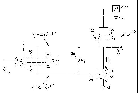
Figure la is a schematic diagram of transistor RIMS device 10. An equivalent
circuit 12 is shown in figure lb. A resonant microbeam 14 is shown as a
grounded
beam structure, in that beam 14 is electrically connected to a reference
terminal or
ground 31. An electrostatic drive electrode 16 and a capacitive sense
electrode 18 are
positioned on opposite sides of beam 14. Sense electrode 18 senses the motion
or
vibration of beam 14 through the change of capacitance between beam 14 and
sense
electrode 18 wherein electrode 18 and beam 14 effectively form the electrodes
of
capacitance CS which varies according to distance between beam 14 and
electrode 18,
during beam 14 vibration. A signal indicating the relationship between beam 14
and
electrode 18 is fed to gate 28 of FET 26. Drive electrode 16 is connected to
drain 24
which is at an output 35 of circuit 10. Output 35 provides a drive signal to
electrode
16 so as to electrostatically drive into motion and sustain vibration of beam
14 at its
resonant frequency. The structure and relationship of drive electrode 16 to
beam 14
and corresponding capacitance cd is like that of sense electrode 18 to beam
14. Drain
24 of FET 26 is connected to one end of a load impedance which consists of a
load
resistor 32 and load capacitor 34 connected in parallel. The other end of the
load
impedance is connected to a voltage supply V+ 33. The values of load resistor
32 and
load capacitor 34 are related to the resonant frequency range of beam 14,
which is
dependent in part on the positive and/or negative tension applied to beam 14.
The
signal at output 35 of circuit 10 is 180 degrees out of phase with its input
at gate 28.
That is so because electrodes 18 and 16 are positioned at opposite sides of
beam 14
rendering the distance relationship of the effective capacitive electrode
pairs 14 and
18, and 16 and 18, respectively, at 180 degrees out of phase. Source 36 of FET
26 is
connected to a reference terminal or ground 31. A feedback impedance 38 has
one
end connected to drain 24 and the other end connected to gate 28 of FET 26.
CA 02205904 1997-05-22
WO 96/18873 PCT/US95/16441
-6-
Feedback impedance 38 provides a certain amount of negative feedback resulting
in a
stabilization of a gate bias to FET 26 so that FET 26 functions in a desired
region of
its performance characteristics. Feedback resistor 38 may be a resistor having
a value
on the order of about 1 p a ohms. The output of circuit 10 may be monitored at
output 35. The description of the present invention is in the context of a
field effect
transistor or transistors; however, the invention also may be implemented with
a
bipolar transistor or transistors, or a combination of field effect and
bipolar transistors.
Figure 1 c shows a circuit 15 like that of figure 1 a except that circuit 15
has a
bipolar transistor 25 instead of FET 26. In lieu of gate 28, drain 24 and
source 36 of
FET 26, there is a base 29, a collector 23 and an emitter 27 of bipolar
transistor 25, in
that order.
Figure 2a shows a top view of a transistor RIMS layout 30 and figure 2b
shows a cross section of RIMS structure 20 having n-type conducting beam 14, a
p-n
junction drive electrode 16 in substrate or underlying epitaxial item 22, and
an ion-
implanted sense electrode 18 in the shell. Although the roles of the two
electrodes, 16
and 18, could be interchanged, the arrangement of figures 2a and b is chosen
because
electrode 16 and substrate 20 have more capacitance to ground, and the
arrangement is
thus more suitable for driving beam 14. Load capacitance 34 is deliberately
increased
by the use of a large drain 24 electrode. Sense electrode 18 should have low
capacitance to ground and is shown as a shallow implant into the undoped
polyshell
which is tied to the gate of adjacent transistor 24. The DC leakage resistance
of the
polysilicon provides a DC bias at gate 28 at the drain 24 potential, but does
not
provide a feedback capacitance that could lower the AC gain because of
negative
feedback. There is a diffusion for source 36 and drain 23, respectively.
The feature of the design shown in figures 2a and 2b is that the conducting
beam 14 provides a ground plane between the sense 18 and drive 16 electrodes.
The
shielding action of the ground plane prevents direct capacitor-coupled voltage
feedback that would lead to oscillation unrelated to mechanical motion of beam
14.
With an ideally grounded beam 14, only the physical movement of beam 14
changes
the sense capacitance and gives rise to an AC voltage on gate 28.
CA 02205904 1997-05-22
WO 96/.18873 PCT/US95/16441
-7-
Figure 3 shows the phase relationships of key signals at the various
components. Feedback resistor 38 can be composed of undoped polysilicon, has a
very high resistance of approximately 108 ohms, and sets the DC voltage of
gate 28 so
that the transistor is turned on at a low current level near a threshold in a
region of
high gain of the transistor performance curve. Displacement x is taken to be
positive
when beam 14 is displaced toward drive electrode 16 (downward in figure 2a).
Positive x displacement means a decrease in the sense capacitance since the
gap of the
sense capacitor is increased. Figure 3 shows the phase relationships of the
various
physical and electrical activities of the RIMS oscillator. Curve 40 reveals
the
displacement x and curve 41 reveals the velocity X. The capacitive change with
respect to the sense capacitance is shown by curve 42. An assumption is that
the AC
impedance of the sense/gate electrode to ground is very high, so that
electrical charges
are constant during a period of oscillation. Thus, a decrease in capacitance
Cs as
shown by curve 42, means an increase in the sense voltage shown by curve 43.
If
there were no capacitive loading (CL = 0), the drain 24 or drive voltage VD
which is
shown by curve 45, would be 180 degrees out of phase with the gate voltage
which is
the same as the sense voltage as shown by curve 43. Also, under such
conditions,
drive voltage 45 is 180 degrees out of phase with the drain current as shown
by curve
44. However, in the actual device, capacitive load 34 is not zero, thereby
causing
drive voltage 45 to lag. Thus, the capacitive component, as shown by curve 46,
of the
drive voltage 45 is in phase with velocity 41 of beam 14, which is the
condition
required to maintain oscillation of beam 14. Figure lb shows an equivalent
circuit of
the invention for purposes of analysis.
The applicable symbols include:
CS = E A` = sense capacitance,
h~+x
Cd = E A`' = drive capacitance,
hd - x
V. = sense DC voltage,
Vd = drive DC voltage,
= complex sense voltage amplitude,
s
vd = complex drive voltage amplitude,
CA 02205904 1997-05-22
WO 96/18873 PCT/US95/16441
-8-
Cg = effective gate capacitance,
CL =1oad capacitance,
Gd = drain conductance,
GL = load conductance,
Yf = feedback admittance (negligible),
m effective mass of microbeam,
k mechanical stiffness of microbeam,
= m~
r = damping coefficient,
4
qS = charge on sense electrode,
qd = charge on drive electrode,
qg = charge on gate electrode,
Im = imaginary part of a complex number, and
hb = beam thickness.
Basic equations include
2 2
mx+rz+kx = qd - qs , (1)
2EaAd 2EoAs
Vd = qd = qd (h`' - x) = drive capacitor voltage,
Cd E.Ad
Vd =-gm"vSZt for a small signal transistor,(2)
V~ = q, = qs (hs x) - sense capacitor voltage,
CS s o A,.
qg =-q, (approximate charge conservation), and
"v CSVS xi = sense voltage. (3)
S (Cg+Cs) (hs+x1)
In a minimum Q analysis, one may derive the condition for resonance, by
assuming a small signal case, and equating the ejwt terms in equation 1.
CA 02205904 1997-05-22
WO 96/18873 PCT/US95/16441
-9-
ZV
a ZVa va C
(-mw2 + jcar + k)xl C
- s so vs
EoAa EoAS
Equate imaginary terms:
wrx, = Cd Vdo Im(vd ) (4)
EoAd
Then combine (2), (3) and (4) to obtain
CdYdo CsVsog~, Im(-Z, )
wrx, _ (hd - x,,) (Cg + CS )(hs + xo ) xi
To obtain a condition for resonance, let co = w o and r mQ
mc,o oz CdVdo CSYo S. Im(-Z, )
Q (hd-xo)(hs+xo) (Cg+Cs)
Let xo hd, hs , to obtain the minimum required Q; wherein
_ (Cg +Cs)khdhs 1
Qmin (5)
CdC., VdoV~ Sn,Im(-Z,)
Since z 1 ' Im(- Z)= ~C',
t = Gd + GL + jwCL , (Gd +GL)z +wzCLz
(Note that equation (5) neglects the electrical feedback through Yf = drain-to-
gate
admittance.)
The following is a numerical example utilizing equation 5, wherein:
CA 02205904 1997-05-22
WO 96/18873 PCTIUS95/16441
-10-
Cg = CS = Cd = Co
h5=he9 A.,.=Ad=2Ab,
hd =h5 =hh = h ,
Vdo = VSa = Vo
k = mw,,2 = pA,,h,,wo2 ,
2 42Ehb2
U~ o = p L4 ,
Gd + GL = GOCL = go
g/
go 1
z
Qmin 4 g
C Vn 2 n '
o gni
4 kh 2 8 42 h 4 Eh2
Qmin - C V 2 ( L E V 2
0 0 0 0
E=1.6-10 m2 ,
,, = 8.85 -10-12 F'm ; and
CA 02205904 1997-05-22
WO 96/18873 PCTIUS95/16441
-11-
with h=1 m and Vo = 1 V,
Eh 2
then =1.81=1010
soV Z
o
so that
4
6. 07 - 1012 b
Qmin
L
If L=100 and =10 , then Qmin = 6, 070.
hb
In another example, yh b =250 and = 0.1 then Qmin = 16, 000. This
example shows that the transistor voltage gain can be less unity, and the
device can
still be self-resonant, because the transistor power gain still exceeds unity.
In the above derivation, the s and d subscripts refer to sense 18 and drive 16
electrodes, respectively. The basic mechanical equation is the equation of
motion 1,
where the force on beam 14 is written in terms of the charges on the drive 16
and
sense 18 electrodes. These charges determine the voltages on the electrodes.
The
assumption of charge conservation leads to equation 3 which relates the sense
voltage
to the displacement amplitude XI. The next set of equations shows how one
leads
directly to an equation for the minimum value of Q, the mechanical quality
factor,
required to maintain the oscillation. Equation 5 shows that decreasing the gap
spacings hs and hd, increasing the transconductance gm of the transistor, and
increasing electrode bias voltages Vdo and Vso minimizes the Q requirement. An
example of the use of this equation is provided next.
There are various configurations which may be implemented. Figures 5a-c
show alternative equivalent circuits for feedback resistor 38. Feedback
resistor 38, of
figure 5a, which is approximately 108 ohms and can be implemented using
undoped
polysilicon, preferably has the polysilicon isolated by nitride to avoid high
impedance
CA 02205904 1997-05-22
WO 96/18873 PCT/US95/16441
-12-
DC paths to ground, especially at high temperatures. In order to prevent drain-
to-gate
feedback, low AC impedance paths to ground should be provided. The capacitance
of
nitride provides such a distributed capacitance 48 as indicated in figure 5b,
but it may
be necessary to provide additional capacitance 50 as indicated in figure 4.
An alternate beam configuration 52 that may offer significant advantages is
shown in figure 6. Configuration 52 uses a twisting or bending mode of beam 54
which has oppositely-located side plates 56 and 53 attached like the wings of
an
airplane. Drive electrode 16 and sense electrode 18 are both located facing
the same
side (i.e., both above or both below wings 56 and 53, respectively, so that
one
capacitor is decreasing while the capacitor on the opposite side is
increasing. Thus,
the phase relationship is the same when electrodes 16 and 18 are located above
and
below the beam as in figure 2. Beam 54 and localized regions of the shell
above beam
54 are grounded, so that there is good electrical isolation between the drive
electrode
16 and sense electrode 18 or between gate 28 and drain 24, as desired. The
above-
provided analysis applies in the case of configuration 52. The potential
advantages of
configuration 52 is that no p-n junction is required under the beam, coplanar
electrodes on the shell are easily connected to the FET, less strain energy in
the beam
for a given shift in the drive or sense capacitance (although less strain
sensitivity), and
reduced end losses and consequently higher Q.
Another embodiment 55 uses a coplanar drive 16 and sense 18 electrodes, as
shown in figure 7. Configuration 55 uses two beams 57 and 59 that are weakly
coupled through the supports at the ends, analogous to a tuning fork. In the
antisymmetric mode of vibration, one beam moves up while the other beam moves
down, and vice versa, that is, 180 degrees out of phase. The above previous
analysis
applies, and resonance can be maintained by a single transistor, by amplifying
and
feeding a signal from sense electrode 16 to drive electrode 18.
Another embodiment 60 is illustrated in figure 8a. Drive electrode 16 and
sense electrode 18 are located on the same side of beam 62, and the two
capacitances
of drive electrode 16 and sense electrode 18 change and are in phase with each
other.
The drive voltage of resonator 60 is opposite in phase to that of the above-
noted
embodiments. Additional stage 64 provides for the needed inverted signal for
the
drive electrode 16. Transistors 66 and 68 are P-channel metal-oxide
semiconductor
CA 02205904 1997-05-22
WO 96/18873 PCT/US95/16441
-13-
(PMOS) devices with a current mirror load which provides the additional phase
change of 180 degrees. Transistor 26 is an n-channel transistor of the same
kind of
process. Load resistor and capacitor are connected between ground and
transistor 68
with a drive electrode connected between transistor 68, and load resistor and
capacitor
70. Complementary metal-oxide semiconductor (CMOS) technology may be used in
the process of fabrication of device 60. Although the basic CMOS process
requires
several additional fabrication steps compared to the N-channel metal-oxide
semiconductor (NMOS) technology process, it provides a higher degree of design
flexibility.
The phase similarity between sense electrode 18 and drive electrode 16 can be
achieved with a source follower 180 of configuration 61 in figure 8b. The
voltage
gain of the source follower 180 circuit is less than one which is sufficient
for an
oscillator having high enough Q, since the current or power gain of this
circuit is
greater than one. Bias resistor 182, having a very large value is connected
between
the drain and the gate of transistor 180, to provide a gate bias. Load
resistor 184
provides a negative feedback to stabilize the bias. Load capacitor 186
provides a
lagging voltage component for driving beam 62 with a proper phase sufficient
for
oscillation. Capacitive sense electrode 18 is connected to the gate, and
electrostatic
drive electrode 16 is connected to the source, respectively, of transistor
180.
Figure 9a is a side cross-section view of a double beam resonant integrated
microbeam sensor 80. The most significant distinction of device 80 from the
above
described microbeam embodiments is the multiple beam structure. Device 80 may
be
micromachined using polysilicon films. Situated in substrate 82 is drive
electrode 76.
Proximate to substrate 82 is lower cavity 84, and adjacent to cavity 84 is a
first
microbeam 72 that is secured at both ends as it is an integral part of silicon
82.
Parallel to first microbeam 72 is a second microbeam 74 which is a beam piggy-
backed to beam 72. Microbeam 74 is secured at both ends as it is micromachined
from the same piece of silicon as microbeam 72. A slit-like medial cavity 86
is
formed between beams 72 and 74. Proximate to beam 74 is sense electrode 78
which
is an integral part of a shell 90 which covers electrode 78 and beam 74.
Between
sensor 78 and beam 74 is an upper cavity 88. Shell 90 provides sealing
integrity in
CA 02205904 1997-05-22
WO 96/18873 PCT/US95/16441
-14-
cavity 88. Cavities 84, 86 and 88 are evacuated and form a common vacuum
chamber.
Figure 9b shows an electronic circuit for double beam RIMS 80. Drive
electrode 76 has a drive voltage signal causing microbeam 72 to vibrate in a
mode at
the resonant frequency of the beam. Beam 74 vibrates at the same frequency
through
mechanical coupling from beam 72. Beams 72 and 74 are connected to ground. The
values of the resonant frequencies indicate an amount of longitudinal tension
placed
on beams 72 and 74 which may indicate a measurement of pressure, acceleration
or
other physical quantity. Sense electrode 78 is proximate to microbeam 74 and
electrically detects the vibration of microbeam 74 and passes a vibration
indicating
signal on to a n-channel transistor 92. Transistor 92 amplifies the vibration
indicating
signal which is coupled with coupling capacitor 94 to a push-pull amplifier
having a
p-channel transistor 96 and a n-channel transistor 98. The common connection
at the
drain of transistor 96 and the drain of transistor 98, is an output 108 which
is
connected to drive electrode 76. The gate of transistor 92 is connected to
high
impedance feedback resistor 102. Resistor 102 is connected to the gate of
transistor
92. The value of resistor 102 is such that biasing of transistor 92 in the
linear region is
maintained. Load resistor 104 and load capacitor 106 are connected in
parallel, and
connect the drain of transistor 92 to a positive (5 to 12 volt) supply V+. The
values of
resistor 104 and capacitor 106 are dependent on the resonant frequency of
microbeams
72 and 74.
Figures l0a-d show a triple resonant integrated microbeam sensor 100. Figure
10a is a side view of the structure of RIMS 100. Device 100 may be
micromachined
from silicon or other like workable material. Situated in substrate 110 is
drive line or
electrode 116 which is proximate to and drives center beam 120. Also situated
in
substrate 110 is sense electrode 114 which is proximate to and senses edge
beam 122,
and sense electrode 118 which is proximate to and senses edge beam 124.
Electrodes
are not shown in figure 10a because of the location of the cut for the cross-
section view,
but are shown in figure l Ob which shows a cross-section view of a cut 90
degrees to that
of figure 10a. Adjacent to drive and sense lines 114, 116 and 118 is a lower
cavity 126.
Next to and above the sense lines, are microbeam segments 120, 122 and 124
which are
in a same silicon layer or plane 132. Beam 120 is shown in figure 10a. Figures
l Ob and
CA 02205904 1997-05-22
WO 96/18873 PCTIUS95/16441
-15-
l Oc illustrate the physical relationship of beams 120, 122 and 124. Adjacent
to beams
120, 122 and 124 is upper cavity 128. Over and sealing the volume, that is,
lower cavity
126 and upper cavity 128, enclosing beams 120, 122 and 124 is shell 130.
Cavities 126
and 128 are maintained in a vacuum. Beams 120, 122 and 124 are each secured at
both
ends of the respective triple microbeam. Center beam 120 has a width that is
typically
twice the width of each of edge beams 122 and 124. Beams 120, 122 and 124 are
isolated from one another and partially from layer 132, by slits 134. Edge
beams 122
and 124 vibrate in phase with each other and 180 degrees out of phase from
center beam
120. Edge beams 122 and 124 mechanically couple vibration from center beam
120.
The resonant frequency of the beams 120, 122 and 124 vary with the tension
exerted on
the beams via the attached ends of the beams. The tension is related to the
magnitude of
the physical phenomenon being measured and indicated by the value of the
resonant
frequency of the beams.
Figure l Od is a schematic of the electronics for triple beam RIMS 100. Sense
electrodes 114 and 118 are connected to the gate of n-channel transistor 136.
Drive
electrode 116 is connected to the output and drain of transistor 136. A high
resistance
feedback resistor 138 is connected between the gate and drain of transistor
136. Load
resistor 140 is connected in parallel with load capacitor 142. Resistor 140
and capacitor
142 connect the drain of transistor 136 to a positive volt supply V+, for
setting the
output level which may be varied.
Figures l la and 1 lb show a microbeam 144 that is connected to substrate 152
at
only one end. Such microbeam structure 150 has application as a temperature
sensor as
the resonance frequency of structure 150 would change with respect to the
temperature
of structure 150. Microbeam structure 150 may also be used as an
electromechanical
filter described above. Drive electrode 146 is situated in substrate 152 for
driving
cantilever beam 144. Cantilever beam 144 is connected to ground and forms an
electrode having capacitance relative to drive electrode 146, that varies
according to
distance between beam 144 and electrode 146. This distance varies as beam 144
moves
or vibrates. Beam 144 is fabricated from a layer 154 with a gap 156. Between
beam
144 and drive electrode 146 is a lower cavity 158. Formed over beam 144 is a
shell 162
with an upper cavity 164. Beam 144 is in a vacuum in the space of upper and
lower
cavities 164 and 158. Sense electrode 148 is situated in shell 162 and has a
capacitance
CA 02205904 1997-05-22
WO 96/18873 PCT/US95/16441
-16-
relative to beam 144, that varies according to distance between beam 144 and
electrode
146. Figure 11a is a view looking at the plane of layer 154 without shell 162
over beam
144, revealing gap 156 that forms cantilever beam 144.
Figure 11 c shows configuration 160 having two cantilever beams 166 and 168
along side each other, formed by gap 170 and situated on substrate 172. The
paired
cantilever beams 166 and 168 are mechanically coupled to each other as drive
electrode
176 drives beam 166 which couples a vibration to beam 168 which vibrates and
is
sensed by sense electrode 178. Electrodes 176 and 178 are situated in
substrate 172.
Configuration 160 has a shell and upper and lower chambers like that of
configuration
150 of figures l la and l lb.
Figure 12a is a schematic of the electronics for the single cantilever beam
144
for use as a temperature sensor. The electronics is similar to that of
configuration 10 in
figure la. Beam 144 is driven by electrode 146 and sensed by electrode 148.
The
resonant frequency of beam 144 varies according to temperature by small shifts
in the
elastic modulus and thus is used as a temperature indicator.
The device of figure 12b is a filter at the resonant frequency of beam 144.
The
signal to be filtered goes to drive electrode 146 to excite beam 144. Signals
having
frequencies other than the resonant frequency of beam 144 do not vibrate beam
144 with
any significance, and thus a negligible signal is detected by sense electrode
148. Signals
having frequencies that are at the resonant frequency of beam 144 easily drive
beam 144
into resonance and sense electrode detects a significant signal which is
amplified by the
associated electronics.
A schematic of the dual cantilever beams and associated electronics is
revealed
by figure 12c. The output of the electronics drives beam 166 at a resonant
frequency
which varies according to the temperature of the beam 166 apparatus. The
vibration of
beam 166, through mechanical coupling, drives beam 168 into a resonant
vibration at a
frequency which is the same as that of beam 166. The vibration of beam 168 is
sensed
by sense electrode 178 which inputs a signal to the electronics. The output of
the
electronics goes to driver 176 to sustain the vibration of beam 166 and in
turn beam 168.
Electrodes 176 and 178 are on the same side of beams 166 and 168. Beams 166
and 168
vibrate 180 degrees out of phase relative to each other, and the sensed
signals are not
only amplified but inverted for sending to drive electrode 176.
CA 02205904 1997-05-22
WO 96/18873 PCT/US95/16441
-17-
A dual microbeam filter sensor is shown in figure 12d. The beam configuration
is the same as that of figure 12c, except the electronics connections to
electrodes 176
and 178 are different in that drive electrode 176 receives the signal that is
to be filtered.
This device is a filter at the resonant frequency of beam 166. The signal to
be filtered
goes to drive electrode 176 to drive beam 166. Signals having frequencies
other than
the resonant frequency of beam 166 do not vibrate beam 166 with any
significance, and
thus the vibration of beam 168 through mechanical coupling is insignificant,
or
nonexistent and an insignificant or no signal is detected by sense electrode
178. Signals
having frequencies that are at the resonant frequency of beam 166 easily drive
beam 166
into resonance and this vibration is coupled to beam 168 which vibrates at
resonance.
Vibration is detected by sense electrode 178 and that detected signal is
inputted to the
gate of transistor 26 for amplification. The output at drain 24 is the signal
that is passed,
which is at the frequency of resonance of beams 166 and 168. The electronics
of the
temperature sensing configurations of figures 12a and 12c are similar to that
of
configuration 10 of figure 1 a. The electronics of the filter configurations
of figures 12b
and 12d are likewise similar except that load capacitor 34 is not incorporated
as it is not
needed because the circuit is merely an amplifier of the sensed vibration of
the beam, as
no oscillator is needed to maintain vibration of the beam.