Note : Les descriptions sont présentées dans la langue officielle dans laquelle elles ont été soumises.
CA 02207231 1997-06-06
PROGRAMMABL$ MEMBRANE SWITCH INPUT/OOTPUT BYSTEM
FIELD OF THE INVENTION
This invention relates to a membrane switch input/output
system utilizing a membrane switch comprising a plurality of
switches for inputting information. More particularly, the
present invention relates to a programmable membrane switch
input/output system having a membrane switch which transmits
signals to and receives signals from a processing device
located remotely from the membrane switch.
BACKGROUND OF THE INVENTION
Membrane switches comprising a plurality of switches have
been used in the past to input information. In general,
membrane switches comprise a circuit or matrix layout embedded
in a plastic film. Switches, generally comprising domes, are
located at specific locations in the plastic film. The matrix
layout comprises a plurality of lines arranged in columns and
rows upon the membrane. The switches are located at the
intersection of a column and row line in the matrix layout such
that when the switches are activated, the two lines in the
matrix layout become electrically connected, decreasing the
resistance between the two lines and thereby indicating that
the corresponding switch has been activated. Domed switches
can be activated by pressing down on the switch to electrically
connect a row line with a column line.
In general, the columns and rows of the matrix layout must
exit the membrane from the same location so that the output
signals generated by activation of the switches can be easily
taken from the membrane switch to a processing device. The
processing device is usually located remotely from the membrane
switch.
The column and row lines of the matrix layout end in
output lines extending from the membrane switch. Pins can be
CA 02207231 1997-06-06
- 2 -
attached to the output lines so that a cable having a connector
at one end can be attached to the pins. The other end of the
cable can then be attached to the processing device.
The processing device is generally the motherboard or
logic board of an electrical element within which the membrane
switch and motherboard are contained. The electrical element
can be, for example, an electrical appliance, such as a
microwave oven, with a membrane switch input/output system to
allow the user to input information which is then sent to the
motherboard of the microwave oven to operate the oven. The
motherboard or logic board will generally contain a
microprocessor to receive the signals from the membrane switch
and send out control signals to operate the electrical
appliance.
One disadvantage of the prior art systems is that the
matrix layout generally has several columns and rows and
therefore has a large number of output lines exiting from the
membrane switch. Therefore, any cable which connects the
membrane switch to the motherboard must have a separate line
or wire for each output line of the membrane switch to transfer
the output signal from the membrane switch to the motherboard.
Clearly, this increases the cost of the system by requiring a
more expensive cable. Also, this requires more space on the
motherboard to connect the cable to the motherboard.
Furthermore, several pins on the input/output chips of the
motherboard must be dedicated to receiving the output signals
from the membrane switch. Both of these features increase the
cost and complexity of the motherboard.
A further disadvantage of the prior art systems is that
the cable, connectors and output lines generally increase the
resistance of the membrane switch. This increased resistance
corrupts the signal by increasing noise and decreasing the
signal during transmission from the membrane switch to the
motherboard.
CA 02207231 1997-06-06
- 3 -
In addition, the switches on membrane switches suffer from
"key rollover" because the switch does not cleanly connect the
row and column lines, thereby often creating multiple erroneous
signals upon each activation of a switch. However, the
membrane switch has no means for cleaning the signal or
debouncing the signal to end key rollover. While these
problems could be corrected at the motherboard, this again
increases the cost of the motherboard. Furthermore, if the
manufacturer of the membrane switch is not the same as the
manufacturer of the motherboard, the manufacturer of the
motherboard may not know what type of filtering or signal
processing are required for the membrane switch.
Some prior art membrane switches comprise LEDs which can
be lit in response to activation of switches. However, to
operate such LEDs, a transistor must be incorporated in the
membrane switch to drive each LED, which increases the cost of
the membrane switch. The prior art membrane switches do not
have a means for activating and powering an LED located on the
2 0 membrane switch from a location of f of the membrane switch, but
not on the motherboard.
In addition, many processing devices, such as
motherboards, are designed to accept a predetermined code,
meaning that a predetermined combination of signals on the
lines being inputted to the motherboard identify activation of
a specific switch on the membrane switch. Generally, the
manufacturer of the motherboard would not also be the
manufacturer of the membrane switch. Therefore, the
manufacturer of the membrane switch must arrange the matrix
layout to conform with the predetermined code required by the
processing device. This often increases the complexity of the
matrix layout in the membrane switch by requiring lines in the
matrix to cross over one another. Each time a line in a
membrane switch crosses over another line, a bridge must be
inserted in the membrane layout to avoid short-circuiting the
two lines, which increases the cost of manufacture of the
CA 02207231 1997-06-06
- 4 -
membrane switch. This problem is compounded when the matrix
layout must avoid a display area in the membrane switch through
which the lines forming a matrix layout cannot pass. In either
case, the membrane switches must be customized so that the
matrix layout provides output signals in the code required by
the processing device. This customization increases costs by
requiring several different types of membrane switches to be
designed and manufactured. Furthermore, an existing membrane
switch cannot be altered or re-wired. Therefore, an existing
membrane switch cannot be changed or re-wired to meet new
requirements, but rather must be replaced if its code is
incorrect or the predetermined code which the processing device
will accept has changed.
SUN~IARY OF THE INVENTION
Accordingly, it is an object of this invention to at least
partially overcome the disadvantages of the prior art. Also,
it is an object of this invention to provide an improved type
of membrane switch input system which can provide a clean
signal from the membrane switch to a motherboard in a code
which can be used by the motherboard but without increasing the
complexity of the matrix layout. It is also an object of the
present invention to provide a membrane switch input system
which utilizes a cable to connect the membrane switch to the
processing device with a number of lines which is less than the
number of output lines of the membrane switch.
Accordingly, in one of its objects, the present invention
resides in a membrane switch input/output system for inputting
information to a processing device comprising: a membrane
switch having a matrix layout and comprising a plurality of
switches located on the membrane switch such that activation
of said switches causes output signals to be generated in a
first code, said output signals indicating which switch was
activated; conversion means electrically connectable to said
CA 02207231 2001-10-30
- 5 -
membrane switch and said processing device for receiving
the output signals from the membrane switch in the first
code and converting output signals from the first code to
a second code for transmission to the processing device;
wherein the first code is dependent on the matrix layout
of the membrane switch and the location of the switches on
the matrix layout; and wherein the second code can be used
by the processing device and is independent of the matrix
layout of the membrane switch and the location of the
switches on the matrix layout.
In a further aspect, the present invention resides in
a method of inputting information from a membrane switch,
having a matrix layout and a plurality of switches to a
processing device, said method comprising the steps of:
(a) generating an output signal in a first code in
response to activation of one of the switches; (b)
converting the output signal from the first code, which is
dependent on the matrix layout of the membrane switch and
the location of the switches on the matrix layout, to a
second code, which is independent of the matrix layout of
the membrane switch and the location of the switches on
the matrix layout; and (c) transmitting the output
signal to the processing device in the second code.
In a still further aspect, the present invention
provides a membrane switch input/output system for
inputting information to a processing device comprising: a
membrane switch having a matrix layout and comprising a
plurality of switches located on the membrane switch such
that activation of said switches causes output signals to
be generated in a first code, said output signals
CA 02207231 2001-10-30
-Sa-
indicating which switch was activated; conversion means
electrically connectable to said membrane switch and said
processing device for receiving the output signals from
the membrane switch in the first code and converting
output signals from the first code to a second code for
transmission to the processing device; light emitting
diodes on the membrane switch; wherein the first code is
dependent on the matrix layout of the membrane switch and
the location of the switches on the matrix layout;
wherein the second code can be used by the processing
device and is independent of the matrix layout of the
membrane switch and the location of the switches on the
matrix layout; and wherein the conversion means comprises
light emitting driving means electrically connectable to
the light emitting diodes for selectively driving the
light emitting diodes in response to input signals from
the processing device.
In a still further aspect, the present invention
provides a method of inputting information from a membrane
switch, having a matrix layout and a plurality of switches
to a processing device, said method comprising the steps
of: (a) generating an output signal in a first code in
response to activation of one of the switches; (b)
coverting the output signal from the first code, which is
dependent on the matrix layout of the membrane switch and
the location of the switches on the matrix layout, to a
second code, which is independent of the matrix layout of
the membrane switch and the location of the switches on
the matrix layout; (c) transmitting the output signal to
the processing device in the second code; (d) repeating
steps (a), (b) and (c) upon each activator of one of the
CA 02207231 2001-10-30
-Sb-
switches; and wherein step (b) of converting the output
signal can only be performed once in a predetermined time
period.
Accordingly, the present invention provides a
membrane switch input system utilizing a conversion means
which is located near the membrane switch. In this way,
the conversion means can convert the output signal from a
first code, corresponding to that generated by the
membrane switch, to a second code which conforms with the
predetermined code of the processing device and can be
used by the processing device. In addition, if the second
code used by the processing device does not require
several lines, the number of lines on the cable and the
space required on the motherboard can be decreased,
resulting in a corresponding cost savings. Furthermore,
the conversion means is located near the membrane switch
so that there is little loss of signal due to resistance
over the cable.
CA 02207231 1997-06-06
- 6 -
In a preferred embodiment, the conversion means can be
programmed with a conversion table to convert output signals
in the first code to the second code. In this way, the
conversion table in the conversion means can be erased and
replaced with a conversion table to convert the output signals
from the first code to a third code different from the first
code or the second code.
A further advantage of the present invention is that the
conversion means can include an LED driver or a seven segment
display driver to power LEDs and displays on the membrane
switch. In this way, additional components, such as
transistors, need not be wired into the membrane switch,
thereby decreasing the cost.
Also, the conversion means can include a signal filter.
In particular, the conversion means could include circuitry to
stop debouncing and end key rollover. This circuitry can be
a timing circuit which limits the number of outputs which could
2o be sent on each output line during a predetermined time period.
This debounces the signal and ends key rollover by eliminating
multiple signals being generated upon each activation of a
switch in a predetermined time period. The predetermined time
period could be a fraction of a second to up to ten seconds
depending on the application.
Further aspects of the invention will become apparent upon
reading the following detailed description and drawings which
illustrate the invention and preferred embodiments of the
invention.
BRIEF DESCRIPTION OF THE DRAWINGS
In the drawings, which illustrate embodiments of the
invention:
CA 02207231 1997-06-06
_ 7 _
Figure 1 shows a top view of a membrane switch;
Figure 2 shows a schematic drawing of a membrane switch
input system according to one embodiment of the invention;
Figure 3A shows an exploded view of a connector
incorporating a conversion unit according to one embodiment of
the present invention;
Figure 3B shows a perspective view of the connector shown
in Figure 3A;
Figure 3C shows a front view of the connector shown in
Figure 3A; and
Figure 3D shows a rear view of the connectors shown in
Figure 3A.
DETAILED DESCRIPTION OF THE PREFERRED EMBODIMENTS
Figure 1 shows a membrane switch, marked generally by
reference numeral 2, which can be used in one embodiment of the
present invention. The membrane switch has a matrix layout 3
shown generally by the lines leading from the switches 4 to the
output lines 5. The output lines 5 are connected to pins 6 and
can send output signals OS when electrically connected to a
connector.
The plurality of switches 4 are located on the membrane
switch 2 in a predetermined pattern depending on the purpose
for which the membrane switch 2 has been created. The switches
4 shown in Figure 1 are dome switches 4 which can be activated
by pressing down on the corresponding switch 4. Activation of
any one of the switches 4 causes an output signal OS to be
generated by bringing into contact the corresponding row line
and column line in the matrix layout 3, decreasing the
CA 02207231 1997-06-06
- g -
resistance between these two lines. The output signal OS
indicating activation of a switch 4 will thus be generated in
a first code C~ by the resistance of the corresponding two
output lines 5 decreasing over the other output lines 5.
It is apparent that which of the output lines 5 show a
decrease in resistance will depend on the matrix layout 3 and
the location of the switch 4 which has been activated on the
membrane switch 2. Thus, the first code C~ is dependent on the
matrix layout 3 of the membrane switch 2 and the location of
the switches 4 on the matrix layout 3. The first code C~ can
of course be varied by changing the matrix layout 3 so that the
output lines 5 corresponding to specific switches 4 exit the
membrane switch at predetermined locations. This can be done,
for example, by arranging the matrix layout 3 so that the lines
corresponding to specific switches 4 lead to specific output
lines 5. However, to accomplish this the number of cross-overs
where two lines on the matrix layout 3 cross-over, one of which
is shown generally by reference numeral 7 in Figure 1,
increases greatly. At each cross-over 7, a bridge must be
formed in the membrane switch 2 to avoid short circuiting the
lines being crossed over. Each time a bridge is required at
a cross-over 7, the cost to manufacture the membrane switch 2
increases. Also, the complexity of the matrix layout 3
increases to provide output signals OS at the output lines 5
having a specific code.
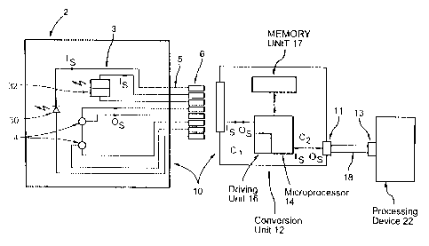
Figure 2 shows a programmable membrane switch input/output
system, shown generally by reference numeral 10, according to
one embodiment of the invention. As shown in Figure 2, the
system 10 comprises the membrane switch 2 and a conversion unit
12. The matrix layout 3 of the membrane switch 2 shown in
Figure 2 has been simplified for purposes of illustration. The
system 10 comprises a conversion unit 12 which is electrically
connectable to the membrane circuit 2. The conversion unit 12
is also electrically connectable to a processing device, shown
generally by reference numeral 22 in Figure 2.
CA 02207231 2001-10-30
-9-
The conversion unit 12 receives the output signals OS
from the membrane switch 2 in the first code C1. The
conversion unit 12 converts the output signals OS from the
first code C1 to a second code Cz which can be used and
understood by the processing device 22. The conversion
unit 12 then transmits the output signal OS in the second
code CZ to the processing device 22. The second code C2
can be any type of code and is independent of the matrix
layout 3 of the membrane switch 2 and the location of the
switches 4 on the matrix layout 3 which generated the
output signals OS.
By using the conversion unit 12, the matrix layout 3
of the membrane switch 2 representing the first code C
can be simplified. For example, the number of circuit
cross-overs 7 can be minimized because the output signals
OS are sent to the processing device 22 in the second code
CZ which is independent of the matrix layout 3 and the
location of the switches 4. In a preferred embodiment,
the second code Cz requires fewer lines to transmit the
output signals OS to the processing device 22 than the
number of output lines 5 required by the membrane switch 2
to transfer the output signals OS to the conversion unit
12. More preferably, the second code C~ transmits the
output signals OS in a serial format, thereby requiring
only four lines, namely two input/output lines, a ground
line and a power line. This decreases the cost of the
cable 18 connecting the conversion unit 12 to the
processing device 22 and also decreases the space or "real
estate" on the processing device 22 which must be
dedicated to the transfer of information into and out of
CA 02207231 2001-10-30
-9 a -
the membrane switch 2. The second code C2 can be
TTL, SPI, I2C or RS232 compatible.
The conversion unit 12 preferably comprises a
microprocessor 14 and a memory unit 17. The memory unit
17 stores a conversion table which can convert output
signals OS from the first code C1 to the second code C2.
In Figure 2, the microprocessor 14 is shown separate from
the memory unit 17, but the conversion table could also be
stored in flash memory
CA 02207231 1997-06-06
- 10 -
located in the microprocessor 14. In a preferred embodiment,
the microprocessor 14 is a C-MOS central processor manufactured
by Atmel having product number SSOP44 and called pin
microprocessor.
Preferably, the memory unit 17 is electrically erasable.
In this way, a conversion table to convert output signals OS
from the first code C~ to the second code CZ can be initially
stored in the memory unit 17. However, if a different membrane
switch 2 or a different processing device 22 is used, the
memory unit 17 can be re-set or re-programmed with a conversion
table to convert the output signals OS from the first code C~
to another code, such as a third code C3 (not shown) . If a
different membrane switch 2 is used which outputs signals OS in
a fourth code C4 (not shown) different from the first code
the memory unit 17 can be re-programmed to convert the output
signals OS from this fourth code C4 to the second code CZ or
another code.
The membrane switch 2 may also contain at least one light
emitting diode 30 or a seven segment display 32. The light
emitting diode 30 and the seven segment display 32 are output
devices which output information to the user of the system 10.
The seven segment display 32 can be formed by seven light
emitting diodes or by a liquid crystal display. In either
case, the light emitting diode 30 and the seven segment display
32 are lit in response to input signals IS from the processing
device 22.
The input signals IS are received by the microprocessor 14
of the conversion unit 12 through the cable 18 from the
processing device 22. Initially, the input signals IS are in
the second code CZ. The conversion unit 12 converts the input
signals IS into the first code C~. This conversion process is
similar to the conversion process for the output signals OS,
and generally utilizes a conversion table stored in the memory
unit 17. The input signals IS are then sent out through the
CA 02207231 1997-06-06
- 11 -
output/input lines 5 of the membrane switch 2. The input
signals IS can travel on separate lines of the matrix layout 3
as shown in Figure 2. Alternatively, the input signals IS can
travel along the matrix layout 3 on lines which are also
connected to the switches 4. In cases where the output lines
5 are used solely to receive input signals IS, these lines can
be referred to as input lines 5. The lines on the membrane
switch 2 which receive the input signals IS and send the output
signals OS will be collectively referred to as output/input
lines 5.
Generally, a transistor must be present on the membrane
switch 2 in order to power a light emitting diode 30 or a seven
segment display 32. However, in a preferred embodiment, the
conversion unit 12 comprises a driving unit 16 which can form
part of the microprocessor 14. The driving unit 16 sends the
input signal IS at a current and voltage level which allows the
light emitting diode 30 to emit light and the seven segment
display 32 to operate. By having the driving unit 16 form part
of the conversion unit 12, the complexity and the cost of
manufacturing membrane switch 2 decreases.
The conversion unit 12 can also comprise filtering means
to filter the output signals OS from the membrane switch 2
prior to transmission to the processing device 22. In a
preferred embodiment, the microprocessor 14 is programmed to
limit the number of output signals OS which can be sent to the
processing device 22 in a predetermined time period. In this
way, the conversion unit 12 prevents key rollover which results
when a single activation of a switch 4 causes multiple signals
OS to be generated. This is often caused by the dome switches
4 because contact of the column and row lines in the matrix
layout 3 is not cleanly made. By limiting the number of output
signals OS which can be sent from the conversion unit 12 to the
processing device 22 during a predetermined time period, such
as 0.1 seconds to 1 second, erroneous output signals OS caused
by key rollover are eliminated.
CA 02207231 1997-06-06
- 12 -
Generally, the membrane switch 2 is located remotely from
the processing device 22. In this case, a cable 18 is used to
transmit the output signals OS to the processing device 22.
However, to decrease the signal loss through the cable 18, it
is preferable to have the conversion unit 12 proximate the
membrane switch 2. In this way, the conversion unit 12
receives the output signals OS before the output signals OS are
sent on the cable 18, avoiding degradation of the output
signals OS by the cable 18, and improving the overall
reliability of the system 10. In addition, because the
conversion unit 12 is proximate the light emitting diode 30 and
the seven segment display 32, any input signals IS sent to the
light emitting diode 30 or the seven segment display 32 will
not loose power due to increased resistance from travelling
over a cable.
Figure 2 shows the output/input lines 5 having pins 6 for
connection to the conversion unit 12. However, it is
understood that the conversion unit 12, comprising the
microprocessor 14 and the memory unit 17, could be located on
the membrane switch 2. In this case, the output/input lines
5 would not terminate at pins 6, but rather would be connected
directly to the microprocessor 14, eliminating the need for
pins 6 entirely.
In the case where the conversion unit 12 is not located
on the membrane circuit 2, it is preferable that the conversion
unit 12 be located in the connector housing 36 of the cable
connector 18 to the membrane switch 2. This embodiment is
shown in Figures 3A, 3B, 3C and 3D.
Figure 3A shows an exploded perspective view of a
connector 34 for connecting a first end 11 of the cable 18 to
the pins 6 connected to the output lines/input 5 of the
membrane switch 2. The second end 13 of the cable 18 can be
connected to the processing device 22. In the preferred
embodiment shown in Figure 3A, the conversion unit 12 is
CA 02207231 1997-06-06
- 13 -
located within the connector housing 36 of the connector 34.
The microprocessor 14 and the memory unit 17 are located on a
circuit contained within the connector housing 36. At the
front end, the connector housing 36 comprises programmable
matrix input/output lines 26 which mate with the pins 6
connected to the output/input lines 5 of the membrane switch
2. The rear end of the connector housing preferably has a
serial input/output port 42 for connection to the first end 11
of the cable 18. The serial input/output port 42 also has a
power and ground connection for supplying power to the
microprocessor 14, the memory unit 17 and any light emitting
diodes 30 or seven segment displays 32 located on the membrane
switch 2.
Preferably, the matrix input/output lines 26 are
programmable by the microprocessor 14. In this way, the
programmable matrix input/output lines 26 coming from the
connector 34 can be programmed to correspond to the
output/input lines 5 from the membrane switch 2. This
increases the versatility of the connector 34 by accommodating
itself to any type of matrix layout 3. It also allows the
designer of the membrane switch 2 to minimize the complexity
of the matrix layout 3 by not being constricted with the
arrangement of the location of the output/input lines 5, or of
the first code C~ of the output signal OS.
Figure 3B shows a perspective view of the connector 34.
Figures 3C and 3D show a front view and a rear view of the
connector 34, respectively.
The present invention also relates to a method of
inputting information from the membrane switch 2 comprising the
steps of generating an output signals OS in a first code C~ in
response to activation of one of the switches 4. The output
signal OS indicates which switch 4 has been activated. The
output signal OS is then converted from the first code C~,
which is dependent on the matrix layout 3 of the membrane
CA 02207231 1997-06-06
- 14 -
switch 2 and the location of the switches 4 on the matrix
layout 3, to a second code C2, which is independent of the
matrix layout 3 of the membrane switch 2 and the location of
the switches 4 on the matrix layout 3. The output signal OS is
then transmitted to the processing device 22 in the second code
The first code C~ is selected to simplify the matrix
layout 3 of the membrane switch 2 and decrease the number of
cross-overs 7. The second code C2 is preferably a serial code
to transfer the output signals OS serially along the cable 18
to the processing device 22.
The above steps can be repeated upon each activation of
one of the switches 4 to successively input information from
the membrane switch 2 to the processing device 22. In a
preferred embodiment, the step of converting the output signals
OS from the first code C~ to the second code CZ can only be
performed once in the predetermined time period to prevent key
rollover.
When the processing device 22 requires the output signals
OS in another code, other than the second code C2, or if the
membrane switch 2 is changed, the conversion unit 12 can be re
set to convert the output signals OS from the first code C~ to
a new code. The conversion unit 12 then transmits the output
signals OS to the processing device 22 in the new code.
It is understood that the processing device 22 can be any
type of device which requires or can process the information
inputted through the membrane switch 2. In a preferred
embodiment, the processing device 22 is a logic board or a
motherboard of an appliance or other electronic device. The
information inputted through the membrane switch 2 can comprise
instructions for operation of the appliance. These
instructions are converted by the conversion unit 12 and sent
to the motherboard for execution by the motherboard. The
motherboard can then send input signals IS through the
conversion unit 12 to the light emitting diode 30 or seven
CA 02207231 1997-06-06
- 15 -
segment display 32 to indicate that the instructions have been
received.
It will be understood that, although various features of
the invention have been described with respect to one or
another of the embodiments of the invention, the various
features and embodiments of the invention may be combined or
used in conjunction with other features and embodiments of the
invention as described and illustrated herein.
Although this disclosure has described and illustrated
certain preferred embodiments of the invention, it is to be
understood that the invention is not restricted to these
particular embodiments. Rather, the invention includes all
embodiments which are functional, electrical or mechanical
equivalents of the specific embodiments and features that have
been described and illustrated herein.