Note : Les descriptions sont présentées dans la langue officielle dans laquelle elles ont été soumises.
CA 02209~93 1997-07-03
WO96/21238 PCT~S96100272
Electron Beam Device with
Single Crystal Window and Matching Anode
Technical Field
The present invention relates to an electron
beam tube having an improved window and anode.
Background Art
Vacuum tubes for generating electron beams have
long been known, as the generation and acceleration of
free electrons is favorably accomplished in a low pres-
sure environment. For example, devices such as televi-
sion picture tubes use accelerated electrons to excitepoints on a phosphorescent screen which thereafter irra-
diate light for viewing.
In order for electron beams to be produced in a
vacuum tube for use outside the low pressure environment
of the tube, windows have been developed which allow
electrons to exit the tube but keep gases at ambient
pressure from entering. Since a beam of electrons pene-
trating such a window can result in heating that destroys
the window, means of cooling such windows have also been
developed.
In U.S. Pat. No. 3,486,060, Swanson teaches the
use of a number of angled orifices for directing laminar
flow of cooling gases across a metal window. U.S. Pat.
No. 3,562,793 to McCann et al. also teaches the use of
laminar gas flow to externally cool metal windows for
charged particles.
U.S. Pat. No. 3,629,576 to Enge describes a
focussing electrode for use in an accelerator tube, the
electrode generally shaped as a plate having a central
aperture through which charged particles pass and a sym-
metric variation of indentations encircling that aper-
ture.
CA 02209~93 1997-07-03
WO 96/21238 PCTnUS96l0n272
In U.S. Pat. No. 3,702,973, Daugherty et al.
describe a laser or ozone generator in which electrons
generated by emission from filaments are accelerated to a
plate held at positive potential, the plate having a plu-
rality of holes that allow some electrons to passthrough, the holes covered with a metal diaphragm through
which some electrons penetrate to reach a gas such as
oxygen. U.S. Pat. No. 3,883,413 to Douglas-Hamilton
discloses the use of such a device with pulsed electron
beams and decaying electric fields. In U.S. Pat. No.
4,095,115, Orr, Jr. et al. disclose a hollow cathode
plasma discharge device utilizing a metal window and
adjacent high velocity oxygen gas for producing ozone.
U.S. Pat. No. 4,409,511 to Loda et al.
describes a phase transition cooling system for charged
particle accelerators, the cooling system involving
directing atomized, vaporizable liquid at charged par-
ticle windows made of metal or plastic. In U.S. Pat. No.
4,468,282, Neukermans teaches a method of making amor-
phous thin film windows for use with ink jet printers.
In U.S. Pat. No. 4,764,947, Lesensky teaches acathode focussing arrangement for production of x-rays by
electrons impinging upon a metal anode. U.S. Pat. No.
4,825,123 to Franzel et al. discloses a method for making
x-ray tubes wherein a cathode cup is manufactured in two
pieces to m;nim;ze damage to the cathode or filament.
U.S. Pat. No. 5,093,602 to Kelly teaches of a
device for atomizing a stream of fluent material which
can use an electron beam directed through an electron
permeable membrane formed of amorphous boron-nitride to
facilitate dispersion of a liquid. In U. S. Pat. No.
5,210,426, Itoh et al. teach of an electron beam device
including an electron permeable window formed of a Ti-Al
composite. Finally, U.S. Pat. No. 5,235,239 to Jacob et
al. teaches of various foil window constructions for a
particle accelerator.
CA 02209~93 1997-07-03
WO96/21238 PCT~S96/00272
A number of applications for which low voltage
electron beams are particularly desirable creates a
desire for further improvements in this area.
Summary of the Invention
The present invention employs single crystal
membranes for electron permeable, gas impermeable windows
and also employs matching crystalline anodes in electron
beam devices. As the cooling needs of such crystalline
membranes differ from those of the metal foil membranes
typical in the prior art, novel cooling devices are also
disclosed.
The orderly crystal lattice of single crystal
membranes permits electrons to more easily penetrate the
membranes than prior art windows made of polycrystalline
or amorphous materials, allowing a lower voltage to be
applied and lower energy electrons to be produced. At
the same time, the orderly crystal lattice of such mem-
branes better prevents molecules of gases or liquids from
penetrating the membranes. The strength of single crys-
tals is also superlative, allowing membranes formed of
such materials to be made thinner, allowing even greater
electron transparency. Such single crystals can also be
formed of elements having a relatively low atomic number,
which reduces scattering of electrons traversing the
membrane. The use of single crystal membranes for elec-
tron windows in beam generating devices thus has a combi-
nation of attributes not found in other types of windows.
Employment of crystalline anodes for electron
beam devices also has a number of advantages. As above,
single crystals offer superior strength, and crystals
such as silicon can be anodically bonded to glass, so
that a crystAll;ne anode can provide a convenient and
strong front end to a glass vacuum tube. Semiconductor
processing techniques can be used to shape such an anode,
so that, in one embodiment, single crystal windows can be
formed simply at etched portions of the anode. On the
other hand, where a window is separately formed from the
CA 02209~93 1997-07-03
WO96/21238 PCT~S96/00272
anode, the anode and window materials can be selected to
have matching coefficients of thermal expansion.
The present invention also involves methods for
making electron beam generating devices with single crys-
tal membranes and anodes. In one embodiment of theinvention, a single crystal membrane is fashioned by
selectively etching a single crystal substrate such as a
silicon wafer to leave a window of desired dimensions.
In another embodiment, a single crystal membrane is grown
on a crystalline substrate having a matching lattice con-
stant which promotes single crystal growth, after which
the portion of the substrate obstructing the window is
etched away. In either of these embodiments the remain-
ing substrate can serve as a means for attachment of the
membrane to the remainder of the vacuum tube device, and
can also serve as the anode. Also, the substrate sur-
rounding the membrane can be etched to form channels for
directing cooling fluid across an outer surface of the
membrane. Similar channels can extend across the mem-
brane, creating an array of extremely thin windows, sepa-
rated by supporting ridges of the same material, which
allows the production of very low energy electron beams.
Thus, for example, a single silicon wafer can be machined
to provide an integral front end, anode, window, cooling
and support structure for a vacuum tube.
Cooling of the membrane can be accomplished
with a variety of techniques. A heat exchanging fluid
can be flowed past the outer surface of the membrane in a
variety of patterns to transport heat away from the
membrane. The fluid can be chosen to have a boiling
point at a temperature and pressure common to that of the
membrane during use, so that heat is absorbed from the
membrane by vaporizing the fluid. A second electron
permeable membrane can be positioned nearby to confine
the flow of fluid to areas near to the membranes, thereby
cooling both membranes. An array of microchannels can
be formed next to the outer surface of the membrane to
direct jets of cooling fluid across the outer surface to
CA 02209~93 1997-07-03
Wos6/21238 PCT~S96/00272
~ -5-
rapidly transport heat from the membrane. The relatively
small thickness and high heat conductivity of the mem-
brane allows cooling of the outer surface to quickly cool
the entire membrane.
The low energy electrons that can be produced
by a beam generating device with such an electron trans-
parent window have a number of useful applications.
Cross linking or incision of polymers can be advanta-
geously performed by a beam having a large number of low
energy electrons. Certain imaging applications can also
be performed favorably with low energy electrons. Gener-
ation of volatile gases such as ozone is also possible
using devices of the present invention, as is atomization
of liquids.
Brief Description of the Drawings
FIG. 1 is a cutaway side view of an electron
beam device of the present invention.
FIG. 2 is a cutaway side view of a top portion
of the device of FIG. 1, oriented normally to the view of
FIG. 1.
FIG. 3A is a top view of a silicon anode of the
present invention.
FIG. 3B is a top view of the anode of FIG. 3A
onto which a substrate including microchannel cooling
slots and a membrane is attached.
FIG. 4 is a top view of the device of FIG. 1
having a membrane with ridges separating recesses.
FIG. 5 is an exploded perspective view of a
front end of an electron beam device formed from a sepa-
rate anode, membrane and ribbed support for the membrane.
FIGs. 6A, 6B and 6C illustrate steps in the
formation of a single crystal membrane and microchannels
of FIG. 3B.
FIG. 7A is a cross-sectional side view of a
pair of single crystal membranes.
FIG. 7B is a cross-sectional side view of
microchannels adjacent to the membranes of FIG. 7A.
CA 02209~93 1997-07-03
WO96/21~8 PCT~S96100272
FIG. 8 is a side view of an electron beam
device including focusing elements and a single crystal
membrane bowed outward prior to evacuation.
Best Mode for Carrying Out the Invention
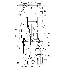
Referring to FIG. 1, an electron beam device 15
is seen to have a vacuum tube wall 18, which may have a
variety of shapes, and is capped by a substrate 19 having
a thin, single crystal, electron permeable, gas imperme-
able membrane 20 at its center. Centered within the tube
wall 18 is an elongated thermionic filament 22 which is
surrounded by a cathode 25, except for an opening of the
cathode 25 facing toward the membrane 20. The filament
22 and the cathode 25 are maintained at a highly negative
potential, which may range from -10 to -200 kilovolts
(kV), relative to the electrical potential of the window,
which is near ground potential. The substrate 19, which
may be made of an n-type silicon wafer, may serve as an
anode attracting electrons from the filament 22.
A number of tube pins 28 penetrate a back end
30 of the device 15 to provide mechanical support and
electrical connections for the filament 22 and the
cathode 25, while maint~;n;ng a gas tight chamber within
the device 15. A filament pin 32 and a second hidden pin
are connected to the body by means of a metal-to-glass
seal or feed-through carrying electrodes 34 and 36, which
are connected within electrically insulative block 38 to
filament 22, in order to generate electrons by thermionic
emission. Support pins 40 and 42 provide support for
block 38 which in turn supports cathode 25. Cathode 25
is provided with an electrical potential at least as
negative as that of the filament 22, in order to acceler-
ate electrons generated at the filament 22 toward the
membrane 20. Wire 44 provides this negative electrical
potential to cathode 25 via a connection not shown in
this figure, wire 44 being connected to cathode pin 46
which protrudes from the back end 30 of the device 15.
The device 15 can be pumped down to a low pressure, such
CA 02209~93 1997-07-03
Wos6/21238 PCT~S96/00272
as 10-4 Torr, after which a glass seal 48 is affixed at
the back end 30.
The membrane 20 is seated atop an opening 50 in
the wall 18. Although not shown to scale in this figure,
the wall 18, which is typically made of glass, is many
times thicker than the membrane 20, which may be less
than 1 to at least 50 microns in thickness, t. Surround-
ing the membrane is a substrate 19 which has an inner
surface that is coplanar with the inner surface 52 of the
membrane 20, but which extends beyond the outer surface
54 of the membrane for strength and attachment to the
wall 18. The substrate 19 may have a thickness t which
is in a range between 1 mm and greater than 1 cm. The
membrane thickness t is ~;n;m;zed in order to allow even
low energy electrons impinging upon an inner surface 52
of the membrane 20 to penetrate the membrane 20 rela-
tively unperturbed and emerge from an outer surface 54
with energy and momentum characteristics that are easily
predicted and manipulated from voltages and currents
provided to the cathode 25 and filament 22. The thick-
ness t, however, cannot be made so small that at pressure
differences and temperatures commonly experienced by the
membrane 20, stresses applied to the membrane 20 exceed
the strength of the material forming the membrane 20.
For this reason, the strength of the material forming the
membrane 20 should be optimized.
It has been found that membranes 20 formed of
single crystals are of high strength and additionally
allow electrons to penetrate relatively unperturbed due
to the ordered atomic arrangement of the crystal lattice
of the membranes 20. To a first approximation, the main
~ obstacles encountered by electrons traveling through
matter are the nuclei of the atoms that form the matter.
In single crystals, these nuclei are arranged in a
lattice that can be thought of approximately as an array
of points aligned on a series of lines. By the same
token, a series of pathways exist that are free of these
lines of obstacles. Electrons traveling in trajectories
CA 02209~93 1997-07-03
WO96121238 PCT~S96/00272
aligned with these pathways have a high probability of
penetrating thin membranes. The interaction of the
atomic nuclei opposing electron penetration increases
with increasing atomic number, and thus it is preferable
for membranes 20 to be formed of low atomic number atoms.
Fortunately, some of the hardest materials known, such as
diamond and single crystal boron nitride, have generally
low atomic numbers of approximately twelve. These
materials also have the favorable characteristics of
behaving generally as electrical insulators but heat
conductors.
Additionally, single crystal membranes 20 have
the advantage of being impervious to gas flow. Gas
molecules, which may be one thousand or more times larger
than electrons, are too large to penetrate the framework
of a single crystal lattice. This is in contrast to
membranes made of polycrystAll;ne materials, in which
defects in the crystal structure may allow gas molecules
to wind through the membranes. Such defects also tend to
propagate during use, promoting failure of the membranes.
Amorphous materials such as metals and glasses also may
allow penetration by some gas molecules, which is one
reason why the glass wall 18 must be made thicker than
the membrane 20.
In general, single crystal membranes 20 of the
present invention are formed of group IV materials, such
as diamond (C), silicon carbide (SiC), single crystal
silicon (Si), single crystal germanium (Ge), or group
III-V materials such as boron nitride (BN), aluminum
nitride (AlN), boron phosphide (BPj, gallium phosphide
(GaP), gallium arsenide (GaAs), gallium nitride (GaN), or
compounds having at least three of these elements. Some
of these materials are commercially available as sub-
strates l9 which can be etched to form single crystal P
membranes 20 of desired dimensions. Other desired
materials can be created by epitaxially growing compounds
that are lattice matched to commercially available,
single crystal substrates, as is known in the art of
CA 02209~93 1997-07-03
WO96/21238 PCT~S96/00272
semiconductor processing. For defect-free single crystal
growth of a membrane 20 to a thickness t that is
preferable for a gas impermeable, electron permeable
window of the present invention, a lattice constant of
the membrane 20 material should match that of the
substrate to within one tenth of one percent. The
substrates l9 can then be etched away, leaving the single
crystal membrane 20 formed of the desired material.
Single crystal materials such as single crystal
silicon can be anisotropically etched as is known in the
art of semiconductor processing to exact ~;~?~ions.
Etching the substrate l9 can be performed to leave a
thicker section of substrate l9 around the membrane 20
for attachment to the glass wall l8 and for added
strength. The thickness of the membrane 20 can be
precisely controlled by implanting an etch stop layer
that will remain after selective etching of the sub-
strate. The etch stop layer also provides a means for
tensioning or compressing the membrane 20, as implanted
ions in that layer may replace atoms of the crystal
lattice having a different bond length. Additionally,
the substrate l9 can be etched to create a channel or
channels that are used during operation to guide fluid
across the outer surface 54 of the membrane 20 for
cooling. Alternatively, a substrate can be etched to
create an array of thin windows separated by thicker
ribs. The strength provided by the ribs allows the
windows to be thinner, allowing penetration by lower
energy electrons.
Referring now to FIG. 2, cathode 25 is seen to
have generally parabolic cross-section in this view (as
compared to the generally rectangular appearance seen in
the perpendicularly oriented view of FIG. l) arching away
from the block 38 and around the filament 22 like petals
of a tulip flower, to focus electrons in a generally
stripe-shaped pattern at the membrane 20. Curves A and B
represent two possible trajectories of electrons emitted
from filament 22 and accelerated by an electric field
CA 02209~93 1997-07-03
W096~1~8 PCT~S96/00272
--10--
between the negative voltage of the cathode 25 and the
ground voltage of the membrane 20. Cathode 25 may have
end walls 58, shown in FIG. 1, which act to focus elec-
trons within the length of the stripe-shaped pattern at
the membrane 20.
The substrate 19, which may be made of doped
silicon similar to that commonly used in semiconductor
wafers, is connected to ammeters 57 and 59, which measure
a current of electrons blocked by the substrate 19. Due
to the relative thinness of the membrane 20 compared to
the substrate 19, a much greater percentage of electrons
impinging on the substrate 19 as compared to those
impinging upon the membrane 20 provide current to the
ammeters 57 and 59, providing a measurement of how
accurately electrons are focused on the membrane 20. The
relative thinness of the membrane 20 as compared to the
substrate 19 also causes the membrane 20 to act as a
resistive barrier to current flow, so that the current in
ammeter 57 can be compared with the current in ammeter 59
to yield a measurement of which side of the substrate 19
more electrons are impinging upon, allowing the electron
beam to be focused accordingly.
FIG. 3A shows a top of a silicon slab 61 which
may be of a similar thickness as the vacuum tube wall 18,
the slab 61 serving as a support bonded to the end of the
wall 18, not shown in this figure. The slab 61 has been
cut with a laser, saw or other machining device to bore a
rectangular hole 62 to allow electrons to pass through.
The slab 61 may be made of doped silicon and may serve as
an anode. The slab 61 is preferably anodically bonded to
the glass wall 18 shown in FIG. 1.
Referring now to FIG. 3B, the substrate 19 and
membrane 20 are mounted atop the slab 61, again
preferably by anodic bonding. For this purpose a thin
film of silicon dioxide sio2 may be grown on either or
both adjoining surfaces of the slab 61 and substrate 19.
The membrane 20 has a smaller area as the hole 62, while
the substrate 19 has a larger area than the hole 62,
CA 02209~93 1997-07-03
WOs6/2l238 PCT~S96100272
allowing the substrate 19 to support the membrane 20
while electrons travel through the hole 62 to impinge
O upon the membrane unperturbed by the slab 61.
The membrane 20 is stripe-shaped in order to
allow a large area for electron tr~nsm;~sion yet, by
minimizing a width w of the membrane relative to its
length 1, stresses of the membrane are lowered at points
along that width, thereby averting failure of the vacuum
chamber. Dispersed along both sides of the length 1 of
the membrane are a series of microchannels 60 which can
be used to direct fluid over the outer surface 54 of the
membrane 20. The microchannels 60 are formed by aniso-
tropic etching of the substrate 19 as is known in the art
of semiconductor processing. The substrate 19 may be
electrically grounded or may be connected to one or more
ammeters.
In FIG. 4, an alternative embodiment of a
single crystal membrane 20 has a series of ridges or ribs
63 that traverse the membrane 20 for added strength,
thereby allowing recesses 64 of the membrane 20 between
the ribs 63 to be thinner. The series of ribs and
recesses is formed by etching similar to the formation of
microchannels. Along the length 1 of the membrane 20,
the recesses 64 are five to ten times as wide as the ribs
63, allowing most electrons impinging upon the membrane
20 to pass through the recesses 64. As before, the
substrate 19 is mounted atop the slab 61, although in
this case the slab 61 has a larger hole to allow for the
larger membrane 20. The recesses 64 may each have
dimensions along the length 1 of the window of about
several hundred ~m and dimensions that span the width w
that may be one to several mm. The ribs 63 each have
dimensions along the width w similar to the recesses 64,
and dimensions along the length 1 that may be one fifth
to one tenth the dimensions of the recesses 64 along the
length. The recesses 64 may have a thickness in a range
between 0.5 ~m and 5 ~m in a direction orthogonal to the
length 1 and width w.
CA 02209~93 1997-07-03
WO 96/21~8 PCT~S96100272
- 12 -
FIG. 5 shows an exploded view of an alternative
embodiment in which an extra layer 56 of silicon or other
compatible material is sandwiched between the slab 61 and
the substrate 19 over the hole 62. The layer 56 has a
5 series of ribs 53 that adjoin and support the thin,
stripe-shaped membrane 20. Having the membrane 20,
support ribs 53 and hole 62 in separate layers as shown
in this embodiment allows for more efficient manufacture,
as the separate layers can be independently sculpted with
different devices and processes. Preferably the slab 61,
the layer 56 and the substrate 19 are all made from
silicon, and the wall is made from Pyrex glass, so that
thermal coefficients of expansion of the different
elements match at common operating temperatures and the
15 electron beam device 15 can withstand a wide range of
temperature variations.
In FIGs. 6A-6C, a process that is used to form
the membrane 20 of FIG. 3B is shown, beginning with FIG.
6A, which shows a crystalline substrate 19 onto which the
membrane 20 is epitA~; Al ly grown. The crystal lattice of
the substrate 19 determines the crystalline structure of
the membrane 20. For that reason the crystal lattice of
the material of the membrane should match that of the
substrate, and while the substrate need not be a single
25 crystal, a surface on which the membrane is grown must
present a defect free crystalline pattern. Given such
lattice matching and a defect free surface, defect free
single crystals can be grown by low pressure chemical
vapor deposition (LP-MOCVD), molecular beam epitaxy (MBE)
30 or other techniques common to the art of semiconductor
processing. In FIG. 6B, which is vertically inverted
relative to FIG. 6A, the substrate 19 has been etched
away across the width w of the membrane 20. In FIG. 6C,
in which the substrate 19 and membrane 20 are oriented
35 perpendicularly relative to FIG. 6B, an array of micro-
channels 60 can be seen to have been anisotropically
etched into the substrate 19 along a length 1 of the
membrane 20.
CA 02209~93 l997-07-03
W O96/21238 PCTrUSg6/00272
-13-
Alternatively, commercially available single
crystal substrates 19 such as silicon can be anisotropi-
cally etched by amounts leaving a membrane 20 of desired
dimensions, and if desired can be etched to create micro-
channels or other structures. In this embodiment, layer
20 in FIG. 6A also represents an etch stop layer in a
doped wafer 19. Such an etch stop layer 20 can be formed
by implanting ions of an opposite conductivity type in
the layer 20 compared to the conductivity type of the
wafer 19. This technique can also be used to provide
tension or compression to a membrane. If, for example,
the wafer 19 is primarily silicon but has been doped with
arsenic ions for n-type conductivity, and the etch stop
layer which will become the membrane 20 has been doped
with boron for a p-type conductivity, the etch stop layer
20 of the crystal lattice will tend to have a smaller
bond length than that of the n-type wafer 19, since boron
has a smaller bond length than that of arsenic. This
will provide tension to the membrane 20, as its bonds are
stretched to conform to the bond length of the mechani-
cally dominant wafer 19. On the other hand, if the
membrane 20 is doped with arsenic and the wafer 19 is
doped with boron, an opposite result will occur, with the
membrane 20 held in compression by the wafer 19.
FIGS. 7A and 7B show an alternative electron
window embodiment of the present invention in which a
second, single crystal, electron permeable, gas imperme-
able membrane 65 and substrate 67 are aligned with mem-
brane 20 and substrate 19. In FIG . 7A the second mem-
brane 65 can be seen to be spaced apart from the first
membrane 20, allowing cooling fluid to flow between the
membranes 20 and 65. The membranes 20 and 65 are so thin
and thermally conductive that cooling of a major surface
rapidly cools an entire membrane. By passing a cooling
fluid between the membranes 20 and 65, the fluid can be
forced to pass closely to a major surface of each mem-
brane, thereby enhancing cooling. FIG. 7B shows a cross
sectional view of membranes 20 and 65 and substrates 19
CA 02209~93 1997-07-03
WO96/21238 PCT~S96/00272
-14-
and 67 of FIG. 7A, with walls of microchannels 60 aligned
with those of microchannels 70 of substrate 67, providing
support and allowing ingress and egress of the fluid to
the space between the membranes 20 and 65.
The plenum formed between the membranes 20 and
65 can be maintained at a pressure between that within
the vacuum tube 15 and an ambient pressure extant outside
the vacuum tube 15. Due to this pressure matching tech-
nique, the membranes 20 and 65 can each be made thinner,
as a pressure differential across each membrane is
lowered, reducing the thickness of the membranes 20 and
65 needed to withstand the stress caused by these
pressure differences.
Cooling of the membrane 20 or membranes 20 and
65 can be performed by a variety of methods. The micro-
channels 60 can be provided with fluid flowing at a high
rate which is directed across the outer surface in a high
velocity flow close to and parallel with that surface 54.
In this fashion, a stagnant, generally non-thermally con-
ductive layer which is common to laminar flow of fluid
adjoining the outer surface and obstructing heat flow
from that surface is not allowed to form. On the other
hand, microchannels 60 disposed around the outer surface
54 can be maintained at a lower pressure than that
adjacent the surface 54, sucking fluid away from the
surface 54 and taking heat acquired by that fluid from
the surface 54 away as well. Cooling fluid can be
introduced to the outer surface 54 near its center, which
is likely to be the part of the surface encountering the
highest current density and the highest heating, thereby
cooling the membrane uniformly as it travels outward
toward the microchannels 60. The microchannels 60 can be
used to supply a small amount of vaporizable liquid to
the outer surface 54 so that a thin film of a liquid
forms on the outer surface 54, particularly if the outer
surface is oriented vertically above the inner surface
52. Thin films of liquid can have favorable heat
exchange characteristics due to vaporization at a
CA 02209~93 1997-07-03
wos6/2l~8 PCT~S96/00272
-15-
meniscus rather than within the film. It is important
that the fluid supplied to the outer surface 54 for
cooling does not leave a residue which hinders operation
of the device 15. High purity inert gases can be used
for cooling, as can high purity water, alcohol, or other
non-viscous liquids. The cooling fluid can be supplied
to the outer surface 54 at a higher pressure than that
distal to the surface 54, so that additional cooling is
performed by the fluid due to expansion of the fluid, in
accordance with known laws of thermodynamics. Any of
these cooling methods can be accomplished with known,
commercially available fluid (gas or liquid) pumps
connected in fluid communication with the various
configurations described adjacent the outer surface 54.
Referring to FIG. 8, another embodiment of the
present invention is shown having a pair of focus plates
78 and some windings of a magnetic coil 80, both of which
can be used to control trajectories of electrons to
better focus the electrons toward the membrane 20. Focus
plates 78 are separated from cathode 25 and can be sup-
plied through pins 82 and 83 with differential voltages
as needed to focus the beam at the membrane 20. Applica-
tion of a DC current to the coil 80 which has an axis
generally coaxial with an imaginary line between the
filament 22 and the membrane 20 will cause electrons
accelerated toward the membrane 20 by the cathode 25 but
angled away from that line to spiral around that line
toward the membrane. Additionally, the magnetic field
generated by a few windings of coil 80 will tend to be
strongest within the coil 80 near the windings, and
weaker near the imaginary line connecting filament 22
and membrane 20, thereby further focussing the electrons
toward the membrane 20.
The membrane 20, which is typically bowed
inward due to the greater pressure outside than within
the vacuum tube device 15, can be seen in this embodiment
to be bowed outward prior to evacuation of the device 15.
Later, when air is evacuated from the device 15 the bowed
CA 02209~93 1997-07-03
WOg6/21~8 PCT~S96/00272
membrane 20 is pulled flat strengthening the membrane 20.
This "prebowing" can be accomplished, for example, by
growing a thin layer of silicon dioxide SiO2 on what is
to become an inner surface of a single crystal silicon
membrane 20 at an elevated temperature.
As the temperature is reduced from the elevated
growing temperature the oxide layer, which has a higher
coefficient of thermal expansion than silicon, shrinks
more than the silicon, causing the membrane 20 to bow
outward due to the compression of the silicon relative to
the oxide layer. When the device 15 is thereafter
brought to a vacuum, the silicon of the membrane 20 is
further compressed as the membrane 20 flattens. The
membrane is further compressed by a similar effect
following anodic bonding of the layer including the
membrane 20 to the glass wall 18, as the wall 18 shrinks
more upon cooling than the membrane 20. The compressed
membrane 20 is found to be stronger than a similar
membrane that is stretched under tension, with the com-
pressed membrane 20 less likely to develop a hole thatpropagates under tension. Other means for compressing
the membrane include selecting the single crystal
membrane 20 material to have a lower coefficient of
thermal expansion than the wall 18 or substrate 19 to
which the membrane is bonded at an elevated temperature,
or implanting the membrane with dopants.