Note : Les descriptions sont présentées dans la langue officielle dans laquelle elles ont été soumises.
CA 02209666 1997-10-02
TITLE OF THE INVENTION
APPARATUS FOR STABILIZING CUT-OFF FREQUENCY USING A
TRANSCONDUCTANCE
BACKGROUND OF THE INVENTION
Field of the Invention
The present invention relates to an apparatus for stabilizing cut-off
frequency
using a transconductance, more specifically, to an apparatus for stabilizing
cut-off
frequency using a transconductance, capable of maintaining constant frequency
characteristics regardless of changes in the temperature, changes in the power
supply
voltage and errors in fabrication, when a filter circuit is installed in an IC
(Integrated
Circuit).
Description of the Related Art
A demand for fabricating a filter into an integrated circuit, which is a
matter of
primary concern in electronics industry, has shown an extreme interest in an
SCF
(Switched-Capacitor Filter) from the end of 1970s. At the present, the SCF
comes in
common use through a MOS IC (Metal Oxide Semiconductor Integrated Circuit)
technology.
CA 02209666 1997-10-02
For fabrication reasons, an active filter constructed with active elements,
typically determines its accurate characteristics by adjusting resistance at
the last
process, which is a serious obstacle to fabricate the active filter into a
complete IC.
A suggestion for overcoming such an obstacle is the SCF consisting of a
switching device, a capacitor, and an operational amplifier. The operation
characteristics of the SCF can be determined by the capacitor ratio that is
suitable for
easy fabrication of the filter into the IC.
Resistance used in the active filter can be substituted with the switching
device
switched by a predetermined switching frequency and the capacitor. The
switching
device can be easily fabricated using an MOSFET (Metal Oxide Semiconductor
Field
Effect Transistor). Accordingly, the integration of the filter is realized.
Fig. IA is a conceptive circuit diagram embodying a resistance using a known
switch 1 and a known capacitor CR. Fig. 1B is an equivalent circuit diagram of
Fig.
lA. The switch 1 is fumed on/offaccording to a predetermined switching
frequency.
Fig. 1 C is a circuit diagram of a real embodiment of Fig. 1 A. Clock signals
in
an inverted phase as compared to each other, are supplied to gate terminals of
transistors Q, and Q,, respectively. The transistors Q, and Q: are then
exclusively
turned on/off. A voltage V, inputted into the circuit is charged and
discharged. As a
result, a filtered frequency voltage V_ is outputted.
When the transistor Q, is turned on, the capacitor CR is charged to CR x V,.
-2-
CA 02209666 1997-10-02
when the transistor Q= is turned on at the same time that the transistor Q; is
turned off,
the capacitor CR is discharged to CR x V,.
The value of the charge q transmitted from the input to the output. is
Q= CR( LZ - L'~j _____________________
The charge q is transmitted for a switching period T~. current i(t) is. on an
average,
1(t~=~ = CR ( L1T' W) _ ~ ~c L? ______ ~,~~
/ CR)
When a resistance corresponding to T~/CR is connected between an input and an
output terminals, Eq. 2 shows the relationship between flowing current and
voltage
drop. Accordingly, an equivalent resistance that is approjcimately calculated
by the
following Eq. 3 is supposed to be connected between the input and the output
terminals.
R' CR f'C' ~ f'= T' .______________
1 1 -<3)
where f is the inverse number of the switching period Tc, i.e., the switching
frequency.
Based on the theory, the resistance that is an obstacle to inte~ation can be
-3-
CA 02209666 1997-10-02
substituted with the switching device and the capacitor.
Fis. ?A is a circuit dia~am of an active filter embodied usins a resistance.
The
active filter consists of: a resistance R~ for controlling an input voltage
V,; an
operational amplifier ? outputting an output voltage Va~~ by amplifying a
signal
generated from the resistance Rr; and a capacitor C, for feeding back the
output from
the operational amplifier ?. The output voltage Vo~~ is,
1
R~C_,
1~
Pout- ;~ v~~ ~=7 1 _____________ s~.~
where w is an angular velocity of an input signal, and f, is a frequency of
the input
sisal.
Fig. 2B is a circuit diagram of an SCF embodied using Fig. lA, consisting of a
switch 1 for sampling an input voltage V, as a predetermined frequency; a
capacitor CR
for charging and discharging the voltage inputted into the switch l; an
operational
amplifier 3 outputting an output voltage Vo,~ by amplifying a signal generated
from the
switch 1; and a capacitor C, for feeding back the voltage of a frequency to be
filtered
out of outputs from the operational amplifier 3. The capacitor CR for charging
and
IS discharging the voltage inputted into the switch l, and the resistance R~
has a
relationship of Eq. 3. The output voltage Vo,~ is,
CA 02209666 2000-08-29
L_CR
:= _ ~ y;.', a=?-.. _________________~~)
where w is an angular velociy of an input signal, and f and f~ are the
frequency of the
input signal and a svy~itchinQ frequency. respectively.
When the tllter circuits of Figs. 2 A and 2B are installed in an IC, the
resistance
and the capacitor cause an error of appro,cimately~20%, respectively, due to a
fabrication error. Therefore, a wanted cut-off frequency for the filter
circuit can be
obtained by changing the switching frequency f . The switching frequency
should be
at least more than nvo times with respect to the frequency of the input sisal
according
to Sampling theory. For a sufficient appro:cimation to the resistance,
typically. a
switching frequency of more than ten times as compared to the frequency of the
input
signal is required.
However, the filter circuit installed in a conventional IC is limited to a low
frequency filter because it cannot include an unlimitedly increased switching
frequency _'
f . Additionally, noise is inevitably generated in the switching frequency f,
which
causes an instability of the circuit.
1~
. CA 02209666 2000-08-29
SUMMARY OF THE INVENTION
The present invention provides an apparatus for stabilizing cut-off frequency
using a transconductance, especially when used in a high-frequency
application. The
apparatus is capable of maintaining constant frequency characteristics
regardless of
noise which may be introduced by a clock frequency, changes in temperature,
changes
in the power supply voltage and errors in fabrication.
In one embodiment the apparatus includes a filtering unit including a
transconductance unit having a variable resistance which is changed when a
transconductance is changed by an inputted control voltage and a capacitor
having a
capacitive reactance. The filtering unit passes supplied input signals only in
a
frequency band determined by the resistance and the capacitive reactance. The
apparatus further includes a transconductance setting unit for making the
transconductance of the transconductance unit variable by supplying a variable
output
signal for use as the inputted control voltage to the transconductance unit.
The variable output signal is changed by a difference in transconductance
between a first transistor connected to a first input of a differential
amplifier and a
second transistor connected to a second input of the differential amplifier. A
controlling unit controls the transconductance of either the first transistor
or the
second transistor.
The transconductance setting unit includes a current mirror, connected to a
power supply, for causing a current to flow through the first input of the
differential
-6-
CA 02209666 2000-08-29
amplifier and the same current to flow through the second input of the
differential
amplifier. The transconductance setting unit further includes a bias voltage
supply for
supplying the first transistor and the second transistor with first and second
bias
voltages respectively. The transconductance setting unit further includes a
transconductance variable unit including a first transistor having a first
transconductance in proportion to the first bias voltage and a second
transistor having
a second transconductance in proportion to the second bias voltage. The
transconductance setting unit further includes a first transconductance
controller,
connected between the current mirror and the transconductance variable unit,
for
generating the control voltage in response to a difference between the first
transconductance and the second transconductance. The transconductance setting
unit
further includes a second transconductance controller, connected to the
transconductance variable unit, for changing the control voltage produced by
the first
transconductance controller by changing a drain-source voltage of the second
transistor to vary the second transconductance.
The filtering unit may comprise a transconductance unit, an operational
amplifier and a capacitor. The transconductance unit may have an input
transistor
having a drain connected to a power supply through a resistance, a gate
through which
the input signal is supplied and a source. The transconductance unit may
further
comprise a transconductance variable transistor having a drain connected to
the
source of the input transistor, a gate through which the voltage for control
is supplied
and a source that is grounded. The transconductance of the transconductance
variable
transistor may be changed according to changes in the voltage for control
received at
the gate. The operational amplifier acts as a filter and has an inverting
terminal that is
-7-
. CA 02209666 2000-08-29
connected to the drain of the input transistor and to one end of the capacitor
which is
commonly connected to the drain of the input transistor and the inverting
terminal of
the operational amplifier. The other end of the capacitor is connected to an
output
terminal of the operational amplifier.
The controlling unit may comprise an external resistance for varying a
transconductance of either the first transistor or the second transistor
according to a
predetermined resistance.
The controlling unit may comprise an external voltage supply terminal for
varying a transconductance of either the first transistor or the second
transistor
according to an inputted adjusting voltage.
The bias voltage supply associated with the transconductance setting unit may
include an operational amplifier having an inverting terminal through which a
direct
voltage is inputted and a non-inverting terminal that is grounded through
first, second
and third resistances. The bias voltage supply may further include a bias
transistor
having a gate that is connected to an output terminal of the operational
amplifier, a
source that is connected to the power supply and a drain that is connected to
the non-
inverting terminal of the operational amplifier through a fourth resistance.
The first
resistance may be 5 KSZ, the second and the third resistances may be 10 KSZ
and the
fourth resistance may be 5 KS~,.
The current mirror of the transconductance setting unit may include a first
current mirror unit having a first current mirror transistor having a source
that is
_g_
CA 02209666 2000-08-29
connected to the power supply, a second current mirror transistor having a
gate that is
commonly connected to a gate of the first current mirror transistor and a
drain of the
current mirror transistor and a source that is connected to the power supply.
The
current mirror may also include a second current mirror unit having a third
current
mirror transistor having a source that is connected to the drain of the first
current
mirror transistor and a fourth current mirror transistor having a gate
terminal that is
connected to a gate terminal of the third current mirror transistor and a
drain of the
fourth current mirror transistor and a source that is connected to the drain
of the
second current mirror transistor.
The first transconductance controller may include a control transistor having
a
source that is connected to the drain of the fourth current mirror transistor
and a drain
that is grounded through the controlling unit. The first transconductance
controller
may further include a control operational amplifier having a non-inverting
terminal
that is connected to an external voltage supply terminal through which the
adjusting
voltage is supplied, an inverting terminal that is connected to the source of
the control
transistor and an output terminal that is connected to a gate of the control
transistor.
The transconductance variable unit may include a first transistor having a
gate
terminal that is commonly connected to the drain of the bias transistor and
the fourth
resistance, a drain that is connected to the source of the current mirror
transistor and a
source that is grounded. The transconductance variable unit may further
include a
second transistor having a gate terminal that is commonly connected to a
location on
the connection of the first and the second resistances, a drain that is
connected to the
source of the current mirror transistor and a source that is grounded.
-9-
CA 02209666 2000-08-29
The second transconductance controller may include a fifth current mirror
transistor having a drain that is connected to the drain of the third current
mirror
transistor, a sixth current mirror transistor having a drain that is connected
to the drain
of the fourth current mirror transistor and a current mirror/output
operational
amplifier, the current mirror/output operational amplifier has a non-inverting
terminal
that is commonly connected to the drain of the third current mirror transistor
and the
drain of the fifth current mirror transistor, an inverting terminal that is
commonly
connected to the drain of the fourth current mirror transistor and the drain
of the sixth
current mirror transistor and an output terminal that is commonly connected to
a gate
of the fifth current mirror transistor and a gate of the sixth current mirror
transistor.
In accordance with another aspect of the invention, there is provided an
apparatus for stabilizing cut-off frequency using a transconductance. The
apparatus
comprises a filtering unit having an input and an output, the filtering unit
including a
transconductance unit for producing a transconductance defining a resistance.
The
transconductance is responsive to an input voltage received at the input and a
capacitor connected to the output and the transconductance unit to implement a
bandpass filter to pass signals from the input to the output, within a
passband defined
by the resistance and the capacitor. The apparatus further includes a
transconductance
setting unit connected to the transconductance unit for setting the
transconductance in
response to current flow through an external resistor connected to the
transconductance setting unit.
-10-
CA 02209666 2000-08-29
The transconductance unit may have a gate terminal for receiving a control
signal from the transconductance setting unit. The transconductance unit may
include
first and second transistors connected in series, the gate terminal being on
at least one
of the first and second transistors. The transconductance setting unit may
include
third and fourth transistors and first and second transconductance controllers
for
controlling transconductance of the third and fourth transistors. The
transconductance
setting unit may include a bias voltage supply, for supplying a bias voltage
to the third
and fourth transistors. The transconductance setting unit may include an
external
control unit, including the external resistor, for controlling the first
transconductance
controller. The transconductance setting unit may include a current mirror for
controlling the second transconductance controller.
The second transconductance controller may include a differential amplifier
and fifth and sixth transistors. The differential amplifier has first and
second inputs
and an output, the first and second inputs being connected to respective
outputs of the
current mirror and the output of the differential amplifier being connected to
gates of
the fifth and sixth transistors. The fifth and sixth transistors are further
connected to
the third and fourth transistors, such that a difference in bias voltage
between gates of
the third and fourth transistors is detected by the current mirror and
amplified by the
differential amplifier, such that the output of the differential amplifier
providing the
control signal received by the gate terminal of the transconductance unit.
-11-
. CA 02209666 2000-08-29
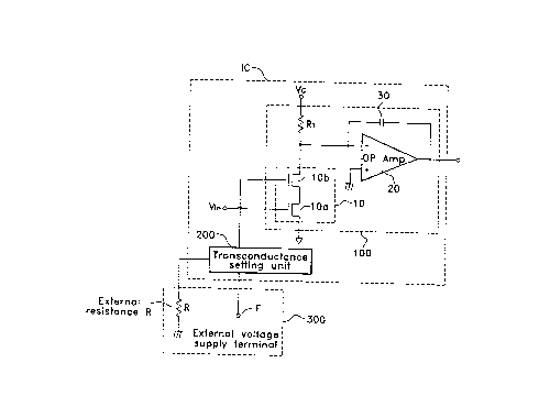
BRIEF DESCRIPTION OF THE DRAWINGS
Fig. lA is a conceptive circuit diagram embodying a resistance using a known
switch and a known capacitor;
Fig. 1 B is an equivalent circuit diagram of Fig. 1 A;
Fig. 1C is a circuit diagram of a real embodiment of Fig. lA;
Fig. 2A is a circuit diagram of a general active filter;
Fig. 2B is a circuit diagram of a filter embodied using Fig. lA;
Fig. 3 is a block diagram of a preferred embodiment of an apparatus for
stabilizing cut-off frequency using a transconductance according to the
present
invention; and
Fig. 4 is a circuit diagram of an embodiment of a transconductance setting
unit
and an external controlling unit of Fig. 3.
-12-
CA 02209666 1997-10-02
DETAILED DESCRIPTION OF THE PREFERRED EMBODIMENTS
An apparatus for stabilizing cut-off frequency using a transconductance.
according to the present invention, will be hereinafter described in detail,
referring to
accompanying drawings.
Fig. 3 is a block diagram of a preferred embodiment of an apparatus for
stabilizing cut-off frequency using a transconductance according to the
present
invention. Referring to the drawing, the cut-off frequency stabilizing
apparatus
includes: a filtering unit 100 for passing only signals having a predetermined
frequency
band; a transconductance setting unit 200 for determining a transconductance
of the
filtering unit 100; and an external controlling unit 300 for controlling a
transconductance of the transconductance setting unit 200.
The filtering unit 100 includes: a transconductance unit 10 that changes the
value of a resistance according to a flowing current; an operational amplifer
20 that
receives and amplifies a signal generated from the transconductance unit 10;
and a
capacitor 30 that feeds back an output from the operational amplifier 20.
Preferably.
the transconductance unit 10 consists of MOSFETs l0a and 1 Ob.
The transconductance setting unit 200, as shown in Fig. 4, includes a bias
voltage supply 210 for supplying a bias voltage; a current mirror 220 for
receiving a
power supply voltage Vpp and outputting the same amount of current to its two
output
~0 terminals A and B; a second transconductance controller 230, connected to
the output
-13-
CA 02209666 1997-10-02
terminals A and B of the current mirror 220, for controlling transconductances
of two
transistors Q, and Q8, and supplying an operation voltage to the
transconductance unit
of the filtering unit 100; a first transconductance controller 240, connected
to the
node B that an output terminal B of the current minor 220, for controlling the
transconductances of the transistors Q~ and Q8 by branching and controlling
the
flowing current: and a transconductance variable unit 250 for varying the
transconductance.
The bias voltage supply 210 consists of an operational amplifer 211 and a
transistor Q9. The operational amplifier 211 has: an inverted terminal(-)
through which
10 a predetermined direct voltage is inputted; a non-inverted terminal(+) that
is grounded
through serially connected resistances R,, R~ and R;; and an output terminal
that is
connected to a gate terminal of the transistor Q9. A source terminal of the
transistor Q9
is connected to a power supply voltage Vpp. A drain terminal of the transistor
Q9 is
connected to a location on the connection of the non-inverted terminal(+) of
the
1 ~ operational amplifier 211 and the resistance R, through a resistance R~.
The current mirror 220 includes transistors Q,, Q,, Q3 and Q,, and makes a
collector current of the transistor Q; the same with a collector current of
the transistor
A source terminal of the transistor Q, is connected to the power supply
voltage
Vpp. A gate terminal of the transistor Q, is connected to a gate terminal of
the
-14-
CA 02209666 1997-10-02
transistor Q=. A drain terminal of the transistor Q, is connected to a source
terminal of
the transistor Q;.
The gate terminal of the transistor Q= is commonly connected to the gate
terminal of the transistor Q, and a drain terminal of the transistor Q=. A
source
terminal of the transistor Q, is connected to the power supply voltage Vpp.
The drain
terminal of the transistor Q~ is connected to a source terminal of the
transistor Q4.
The source terminal of the transistor Q; is connected to the drain terminal of
the
transistor Q,. A gate terminal of the transistor Q3 is connected to a gate
terminal of the
transistor Q~. A drain terminal of the transistor Q3 is connected to the node
A that is a
non-inverted terminal(+) of an operational amplifier 231.
The gate terminal of the transistor Q,~ is connected to the gate terminal of
the
transistor Q3 and a drain terminal of the transistor Q~. The source terminal
of the
transistor Q; is connected to the drain terminal of the transistor Q=. The
drain terminal
of the transistor Q, is connected to the node B that is an inverted terminal(-
) of the
1 ~ operational amplifier 231.
The second transconductance controller 230 includes the operational amplifier
231, a transistor Q5 and a transistor Q6.
A non-inverted terminal(+) of the operational amplifier 231 is connected to
the
drain terminal of the transistor Q;. An inverted terminal of the the
operational
amplifier 231 is connected to the drain teminal of the transistor Q;. An
output terminal
-15-
CA 02209666 1997-10-02
of the operational amplifier 231 is connected to the transconductance unit 10
of the
filtering unit 100.
A drain terminal of the transistor QS is commonly connected to the drain
terminal of the transistor Q; and the non-inverted terminal(+) of the
operational
amplifier 231. A gate terminal of the transistor Q; is commonly connected to
the
output terminal of the operational amplifier 231 and a gate terminal of the
transistor
Q6. A source terminal of the transistor Q; is connected to a drain terminal of
a
transistor Q,.
The gate terminal of the transistor Q6 is commonly connected to the output
terminal of the operational amplifier 23 l and the gate terminal of the
transistor Q;. A
drain terminal of the transistor Q6 is commonly connected to the drain
terminal of the
transistor Q, and the inverted terminal of the operational amplifier 231. A
source
terminal of the transistor Q6 is connected to a drain terminal of a transistor
Qg.
The first transconductance controller 240 consists of a transistor Q,o and an
operational amplifier 241. A source terminal of the transistor Q,o is
connected to the
node B that is the drain terminal of the transistor Q,. A gate terminal of the
transistor
Q,o is connected to an output terminal of the operational amplifier 241. A
drain
terminal of the transistor Q,o is connected to an end of an external
resistance R. A non-
inverted terminal(+) of the operational amplifier 241 is connected to an
external
voltage supply terminal E for controlling the transconductance. An inverted
terminal
-16-
CA 02209666 1997-10-02
(-) of the operational amplifier ?=~l is connected to the drain terminal of
the transistor
Q,~. The output terminal of the operational amplifier 2-tl is connected to the
gate
terminal of the transistor Q,~.
The transconductance variable unit 2~0 includes transistors Q; and Qs. A gate
terminal of the transistor Q, is connected to a drain terminal of the
transistor Q9. The
drain terminal of the transistor Q; is connected to the source terminal of the
transistor
Q;. A source terminal of the transistor Q- is grounded. A gate terminal of the
transistor Qs is connected to a node D that is on the connection of the
resistances R,
and R,. A drain terminal of the transistor Qs is connected to the source
terminal of the
transistor Q6. A source terminal of the transistor Qs is grounded.
The operation of the cut-off frequency stabilizing apparatus according to the
present invention will be described in detail.
First. a brief description on the theoretical basis that a cut-off frequency
can be
stabilized by adjustin' the transconductance of a transistor will be given
prior to the
1 ~ description of the operation of the cut-off frequency stabilizing
apparatus.
Conductance corresponds to the inverse number of resistance. For description
purposes, a FET(Field Effect Transistor) is taken as an example.
The conductance gm of the FET is.
aIo ______________________
g~= a vys -______________
-17-
CA 02209666 1997-10-02
l
where ID is a drain current on a bias point, and Vas is a voltage bet<veen a
gate and a
source.
The transconductance a.~ of the FET corresponds to a slope on an operation
point Q in a FET transmission cuwe. When the transconductance is varied by a
voltage on a circuit. an analogous effect can be obtained that the resistance
is varied.
The effect is called as VVR (Voltage-Variable Resistance) effect.
Referring to an Ip-Vps output curve of the FET (where Vps is a voltage between
a drain and a source), it is noted that when Vps is smaller, the output curve
is almost
straight and the slope thereof depends on VGS.
In other words. this suggests that when the FET operates in a linear area. it
is
possible to electronically waw the resistance by varying Vas.
Direct current resistance Ras bet<veen a drain and a source is,
I h _________________
-grn -____
As shown in Eq. 7, the inverse number of the direct current resistance Ros in
the linear
area with respect to a given Vas is the same with the transconductance gm in
the linear
area with respect to VGS. Therefore, it is possible to vary the resistance by
varying the
voltage of either VGS or Vps. The VVR effect is realized using this.
As shown in Fig. 3, an external resistance R and an external voltage supply
terminal F of an external controlling unit 300 are installed on the outside of
an IC after
-18-
CA 02209666 1997-10-02
r
a filtering unit 100 and a transconductance setting unit 200 are installed in
the IC. A
wanted stabilized cut-off frequency can be obtained by controlling the
transconductance as bellow. regardless of changes in the temperature, changes
in the
power supply voltage, and errors in fabrication when a filter circuit is
installed in the
IC.
First, 2.~ volt is supplied to the inverted terminal(-) of the operational
amplifier
211 in the bias voltage supply 210. At this time, the non-inverted terminal(+)
of the
operational amplifier 211 becomes 2.5 volt, which is a charateristic of the
operational
amplif er 211. The voltage on the respective ends of the serially connected
resistances
is divided by the respective resistance ratio. As a result, the node C becomes
3 volt
and a node D becomes 2 volt.
Voltages generated from the nodes C and D are supplied to transistors Q, and
Qg, respectively.
The transistors Q, and Qg have the same charateristics, and 1 volt difference
1 ~ exists between voltages supplied to their respective gate terminals.
Accordingly, a
current h flowing through the transistor Q~ is larger than a current I;
flowing through
the transistor Q8, and therefore, a voltage of the node A becomes larger than
a voltage
of the node B.
The current flowing through the transistors Q~ and Qs is supplied from the
node
?0 A and the node B which are two output terminals of the double constructed
current
-19-
CA 02209666 1997-10-02
mirror 220.
At this time, a voltage difference between the voltages of the nodes A and B
is
amplified by the operational amplifier 231 and outputted to the output
terminal in order
to compensate the voltage difference between the nodes A and B. As a result,
voltages
of the gate terminals of the transistors Q; and Q6 connected to the output
terminal of
the operational amplifier 231 are also increased.
When the voltages of the gate terminals of the transistors Q; and Q6 are
increased, the voltages of the source terminals of the transistors QS and Q6
are,
accordingly, increased having a voltage difference of a threshold voltage
Consequently. the voltage Vps that is a voltage between the drain terminals
and
the source terminals of the transistors Q, and Qs is increased, thereby
increasing
current.
In other words. since the transconductance is an inverse number of the
resistance, the possibility that the transconductance can be varied implys the
possibility
I S that the resistance can be controlled to have a desirable value.
Therefore, the
transconductance of the filtering unit 100 is varied to have a desirable value
by
connecting the output terminal of the operational amplifier 231 that is the
output
terminal of the transconductance setting unit 200 to the gate terminal of the
transconductance unit 10 of the filtering unit 100. Thereby, it is possible to
construct a
'_'0 stabilized filter circuit, even when the capacity of the capacitor
included in the filtering
-20-
CA 02209666 1997-10-02
unit 100 is changed in the range of t20%.
The transconductance can be varied to have a wanted value by controlling the
current I, flowing out according to the voltage difference bet~.~een the
voltages of the
nodes A and B.
The current I, can be controlled by varying the external resitance R located
out
of the IC. By controlling the current I,, the transconductace can be
controlled.
When the value of the external resistance R is made smaller. the current
flowing
through the resistance R is increased. As a result, the drain voltage of the
transistor Q6
is dropped. The drain voltage of the transistor Q8 of the transconductance
variable unit
250 is also dropped. Consequently, the transconductance of the transistor Qs
is
dropped.
At this time, the operational amplifier 231 amplifies the voltage difference
between the nodes A and B and outputs the amplified voltage to the output
terminal
OUT. The amplified and outputted voltage is supplied to a gate terminal (not
shown)
of the transconductance unit 10 of the filtering unit 100. Accordingly, the
transconductance can be controlled to have a wanted value. When a resitance
having a
1% error is used as the external resistance, the filter can be designed to
have a 1%
error.
Additionally, when the voltage supplied to the external voltage supply
terminal
?0 E of the second transconductance controller 240 is controlled, the voltage
of the node
-21-
CA 02209666 1997-10-02
E is varied. As a result, the current flowing through the external resistance
R is also
varied, and therefore, the transconductance of the transistor Qg can be varied
in the
same manner that the value of the resitance is varied. Bv controlling the
output of the
operational amplifier 231, the transconductance unit 10 of the filtering unit
100 can be
varied. and a filter construction having a wanted frequency band and a wanted
amplification can be obtained.
When the output of the operational amplifier 231 is inputted through the gate
of
the transistor l Ob, the output of the operational amplifier 231 is varied.
The gate
voltage then is varied, and the transconductance of the transistor l Ob is
accordingly
varied. Therefore, it is possible to design a filter capable of passing only
wanted
signals out of signals inputted through the transistor 10a.
The apparatus for stabilizing cut-off frequency using transconductance
according to the present invention is not restricted to the above filter
circuit, and it is
clearly understood that many variations may be made within the scope and
spirit of the
1~ present invention by anyone skilled in the art. For example, if the feed
back capacitor
30 of the filtering unit 100 is substituted with a resistance, the apparatus
can be used to
an amplification circuit without any degradation of the performance.