Note : Les descriptions sont présentées dans la langue officielle dans laquelle elles ont été soumises.
CA 02210822 1997-07-17
-1-
SIMPLIFIED INTERFACE TO A TIME-DIVISION
MULTIPLEXED COMMUNICATIONS MEDIUM
Technical Field
This invention relates to time-division multiplexed communications
systems, including time-slot interchange systems.
Background of the Invention
Various modern-day telecommunications switching systems use a time-
division multiplexed (TDM) communications medium as their switching fabric. An
illustrative example of such systems is the Lucent Technologies Inc. Definity~
private branch exchange (PBX). Port circuits that interface communications
links
and devices (applications) to the TDM medium normally provide access to only a
relatively small number of the medium's time slots. For example, the port
circuit
packs of the Definity PBX provide access to any 32 time slots of the PBX's 256
time-slot TDM bus. Applications that need access to more than 32 time slots
either
use multiple port circuit packs or custom (and generally complex and
expensive)
time-slot interchange (TSI) circuits.
Applications that require access to more time slots than conventional
port circuits provide, are becoming ever-more common. If such applications use
multiple port circuit packs, they consume multiple circuit-pack slots on the
TDM
medium and thereby reduce the number of applications that the switching system
can
serve. If such applications use custom complex and expensive TDM interface
circuits, they significantly increase the system's cost.
An ideal TDM interface would provide each application served by a port
circuit pack access to all of the TDM medium's time slots that the application
requires, in a simple, low-cost, manner.
Summary of the Invention
This invention is directed to avoiding the disadvantages and meeting the
desires of the art. Illustratively according to the invention, a processor
that executes
applications which require access to time slots of a TDM medium uses spare
processing capacity and/or spare hardware of the processor to interface to the
TDM
medium and to implement a time-slot-interchange (TSI) function. The resulting
interface to the TDM medium is simple and low-cost; for processors that have
sufficient excess processing capacity and spare peripheral elements, the cost
is
effectively zero. The processor has a control store that stores a bit map of
the time
slots of the TDM medium. The bit map is either examined by the processor
during
each time slot, or preferably is used by circuitry -- such as spare internal
peripheral
elements of the processor -- to generate interrupts, to indicate to the
processor which
CA 02210822 1997-07-17
-2-
time slots to access. In the latter, interrupt-based, configuration, the
processor
advantageously does not waste processing on time slots which it will not be
accessing. In either case, the processor advantageously has the capability of
accessing any time slots of the TDM bus, as specified by the bit map. The
processor
has a read buffer and a write buffer for effecting data transfers between the
TDM
medium and the applications. The applications have random access to the
buffers,
thereby effecting a time-slot-interchange function.
Generally according to the invention, an interface to a TDM medium
which transports data in time slots that are grouped into frames comprises a
processor for executing functions (applications) that either use data from
first time
slots of the frames of the TDM medium or generate data for second time slots
of the
frames of the TDM medium. Same said processor tracks occurrence of the time
slots
and the frames of the TDM medium and either receives data from the first time
slots
of the frames of the TDM medium for use by the functions or transmits data
generated by the functions in the second time slots of the frames of the TDM
medium. Hence, the application-execution and interface functions are performed
by
the same processor, with the help of little or no additional hardware,
resulting in a
simple and low-cost interface.
According to one aspect of the invention, the processor includes a
control store for storing a time-slot map of the frames of the TDM medium
identifying either the first time slots or the second time slots, and the
processor
responds to each occurrence of a time slot on the TDM medium by determining
from
the time slot map whether the occurring time slot is a first time slot or a
second time
slot. This implementation advantageously requires no hardware in addition to
the
processor.
According to another aspect of the invention, the interface further
includes a control store for storing a time slot map of the frames of the TDM
medium identifying either the first time slots or the second time slots, and
circuitry
associated with the control store for indicating to the processor that a
presently-
occurring time slot is identified in the time slot map as either a first time
slot or a
second time slot. The processor responds to an occurrence of a time slot on
the
TDM medium only when the circuitry indicates that the presently-occurnng time
slot is identified as either a first time slot or a second time slot.
Depending on
whether the control store and/or associated circuitry are external or internal
to the
processor, this implementation may or may not require hardware in addition to
the
processor. However, this implementation advantageously frees the processor
from
performing processing for time slots that it does not access.
CA 02210822 1997-07-17
-3-
Preferably according to the invention, the processor includes a plurality
of data storage locations (e.g., a buffer) for temporarily storing the
received data or
the generated data, and the processor accesses the storage locations in any
order,
whereby the processor effects a TSI function.
These and other advantages and features of the invention will become
more apparent from the following description of an illustrative embodiment of
the
invention taken together with the drawing.
Brief Description of the Drawing
FIG. 1 is a block diagram of a first illustrative implementation of a TDM
bus interface that embodies the invention;
FIG. 2 is a functional flow diagram of TDM bus interface operations of
the interface of FIG. 1;
FIG. 3 is a block diagram of a second illustrative implementation of the
TDM bus interface;
FIG. 4 is a functional flow diagram of the TDM bus interface operations
of the interface of FIG. 3;
FIG. 5 is a block diagram of a third illustrative implementation of the
TDM bus interface; and
FIG. 6 is a block diagram of a fourth illustrative implementation of the
TDM bus interface.
Detailed Description
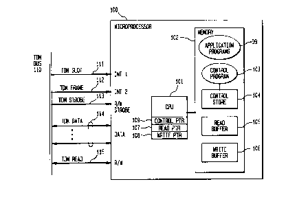
FIG. 1 shows a first illustrative embodiment of a TDM bus interface
constructed according to the principles of the invention. The TDM bus
interface of
FIG. 1 is implemented by a conventional microcontroller or microprocessor 100
connected to TDM bus 110. TDM bus 110 illustratively defines repeating frames
each comprising 256 time slots. A TDM SLOT signal line 111 which clocks
individual time slots is connected to a first interrupt input (INT 1 ) of
microprocessor
100. A TDM FRAME signal line 112 which clocks individual frames is connected
to a second interrupt input (INT 2) of microprocessor 100. (Alternatively,
polled
input/output (I/O) connections to microprocessor 100 may be used instead of
the
interrupt connections.) A TDM STROBE signal line 113 which indicates that data
on TDM DATA bus 114 are stable and ready to be latched is connected to an R/W
STROBE input and output of microprocessor 100. The eight leads of the byte-
wide
TDM DATA bus 114 are connected to the DATA inputs and outputs of
microprocessor 100. And a TDM READ signal line 115, whose state indicates
whether the TDM bus 110 is to be read or written, is connected to an R/W input
and
output of microprocessor 100.
CA 02210822 1997-07-17
-4-
Microprocessor 100 comprises a central processing unit (CPU) 101 and
an internal memory 102, as is conventional. A block of words in memory 102
that
together comprise 256 bits forms a control store 104. Control store 104
contains a
bit map of the time slots of TDM bus 110, with bits set for only those time
slots that
microprocessor 100 will use, and bits cleared for unused time slots. A control
pointer 109 defined by CPU 101 points to a present position in control store
104. A
block of words in memory 102 that together comprise 256 bytes forms a read
buffer
105, and another such block forms a write buffer 106. A read pointer 107 and a
write pointer 108 defined by CPU 101 point to present positions in buffers 105
and
106, respectively. Memory 102 also stores a control program 103 for execution
by
CPU 101. As is conventional, memory 102 also stores application programs 99
for
execution by CPU 101 --their particulars are not relevant to the invention.
The operation of control program 103 is shown in FIG. 2. Execution of
control program 103 is initially invoked upon receipt of a TDM FRAME signal at
the INT 2 input of microprocessor 100. Upon receipt of the TDM FRAME signal
indicating the end of one frame and the beginning of a next frame, at step
200,
program 103 resets pointers 107-109, at step 202. Resetting of each pointer
107-109
causes that pointer to point to the beginning --the first bit in control store
104 and the
first byte in read buffer 105 and write buffer 106-- of the pointer's
corresponding
area 104-106 of memory 102. Program 103 then ends its execution, at step 204.
Execution of program 103 is next invoked by receipt of a TDM SLOT
signal at the INT 1 input of microprocessor 100, at step 206, indicating the
end of
one time slot and the beginning of a next time slot. In response, program 103
reads
the control store 104 bit that is pointed to by control pointer 109, at step
210.
Program 103 then checks the state of this bit, at step 214. If the bit is
cleared,
indicating that the application or applications which are served by
microprocessor
100 do not use the present time slot, program 103 merely increments control
pointer
109, at step 230, and ends its execution, at step 232. But if the control bit
is found to
be set at step 214, indicating that the applications served by microprocessor
100 do
use the present time slot, program 103 checks the state of TDM READ line 115,
at
step 216, to determine if TDM bus 110 is to be read or written. If TDM bus 110
is to
be read, program 103 causes microprocessor 100 to latch data from TDM DATA bus
114 upon occurrence of a strobe signal on TDM STROBE line 113, at step 218.
Program 103 then causes microprocessor 100 to write the latched data into a
location
of read buffer 105 that is pointed to by read pointer 107, at step 220.
Program 103
then increments read pointer 107, at step 222, and proceeds to steps 230 et
seq.
CA 02210822 1997-07-17
-5-
If it is determined at step 216 that TDM bus 110 is to be written,
program 103 causes microprocessor 100 to read a location of write buffer 106
that is
pointed to by write pointer 108, at step 224. Program 103 then increments
write
pointer 108, at step 226, and causes microprocessor 100 to transmit the data
that was
read from write buffer 106 onto TDM DATA bus 114 upon occurrence of a strobe
signal on TDM STROBE line 113, at step 228. Program 103 then proceeds to steps
230 et seq.
Execution of program 103 is invoked again at each occurrence of a
TDM FRAME or a TDM SLOT signal, at step 200 or step 206, respectively.
Execution of other programs --e.g., application programs or input and
output programs-- by CPU 101 results in reading of read buffer 105 and writing
of
write buffer 106. Locations of buffers 105 and 106 are randomly accessible to
CPU 101, whereby a time-slot interchange (TSI) function is performed by
microprocessor 100.
If microprocessor 100 has sufficient spare processing capacity to
execute control program 103 in addition to its other tasks (e.g., execution of
application programs 99), the interface's embodiment of FIG. 1 has zero
hardware
cost. However, it does require microprocessor 100 to perform control-program
103
processing during each TDM time slot to determine if it is to use the present
time
slot. In most applications, processor 100 is likely to use only a small
fraction of all
of the time slots of TDM bus 110. Hence, processing required for unused time
slots
consumes a large fraction of the control-program 103 processing.
FIG. 3 shows a second illustrative embodiment of the TDM bus
interface, which lessens the control-program-processing load on microprocessor
100
by eliminating all control-program processing for unused time slots. The
interface
of FIG. 3 differs from the interface of FIG. 1 in that an external control
memory 300
and associated control circuitry 301-302 take the place of control store 104
and
control pointer 109, and a control program 303 takes the place of control
program 103.
TDM SLOT signal line 111 is connected to a data input of a counter
301. A RESET input of counter 301 is connected to TDM FRAME signal line 112.
Counter 301 increments its count at each occurrence of a TDM SLOT signal, and
resets its count at each occurrence of a TDM FRAME signal. The count of
counter
301 is connected to an ADDRESS input of a first port of a dual-port control
memory
300. A read/write input of the first port of control memory 300 is permanently
set in
the READ state. The contents of control memory 300 are the same as those of
control store 104 of FIG. 1. Hence, control memory 300 takes the place of
control
CA 02210822 2000-11-20
-6-
store 104, while counter 301 takes the place of control pointer 109 of FIG. 1.
The DATA
output of the first port of control memory 300 is connected to one input of an
AND gate
302, while TDM SLOT signal line 111 is connected to a second input of AND gate
302.
The output of AND gate 302 is connected to the INT 1 interrupt input of
microprocessor
100. Hence, microprocessor 100 receives an interrupt at the INT 1 input only
when the
contents of control memory 300 indicate that the present time slot indicated
by the TDM
SLOT signal is to be used by microprocessor 100. The address (ADDR), data
(DATA),
and read/write (W) inputs of the second port of control memory 300 are
connected to
microprocessor 100 such that microprocessor 100 is able to reprogram the
contents of
control memory 300.
The operation of control program 303 is shown in FIG. 4. Execution of
control program 303 is initially invoked upon receipt of a TDM FRAME signal at
the INT
2 input of microprocessor 100, at step 400. In response, program 303 resets
pointers 107
and 108, at step 402, and then ends its execution, at step 404.
Execution of program 303 is next invoked by receipt of an interrupt at the
INT 1 input, at step 406. In response, control program 303 proceeds to perform
the TDM
bus 110 read or write operations of steps 216-228 which were described in
conjunction
with FIG. 2. Control program 303 then ends its execution, at step 408.
Execution of program 303 is invoked again at each occurrence of a TDM
FRAME signal or receipt of an interrupt at the INT 1 input, at step 400 or
step 406,
respectively.
Port circuits of many telecommunications switching systems are equipped
with digital signal processors (DSPs). FIG. 5 shows a third illustrative
embodiment of the
TDM bus interface which makes use of otherwise-unused components and
processing
capacity of a DSP 500 of a port circuit. DSP 500 is illustratively the DSP
56303 of
Motorola~ Inc. Semiconductor Division. For simplicity and clarity of
presentation, only
those elements and functions of DSP 500 that are relevant to an understanding
of the
invention are shown in FIG. 5 and described below.
DSP 500 includes a host interface 510, a spare serial-data (ESSI) interface
511, three spare direct memory access (DMA) units including units 516 and 517
(out of a
total of six that are included in the Motorola DSP 56303), a program random
access
memory (RAM) 518 which stores application programs 99, a memory RAM 502, a
program-control section 501 (that in the Motorola DSP includes a program
interrupt
controller, a program decode controller, a program address generator, a data
arithmetic and
CA 02210822 2000-11-20
_7_
logic unit, a memory access controller, accumulators, and a shifter) that
executes programs
from program RAM 518, and an external bus interface 513 to an external bus
514.
Elements 501, 502, 510, 511, 513, and 516-518 are interconnected by an
internal bus 519.
TDM SLOT signal line 111 is connected to an SCKO (serial clock) input of
ESSI interface 51 l and to an IRQB (DMA request external interrupt) input of
DMA unit
517. TDM FRAME signal line 112 is connected to an SC02 (serial control) input
of ESSI
interface 511 and to an IRQA input of DMA unit 517. An SCOT output of ESSI
interface
511 is connected to an HCS (host chip select) input of host interface 510. TDM
STROBE
signal line 113 is connected to an HDS (TDM strobe) input of host interface
510. TDM
DATA bus 114 is connected to HD[0-7] (TDM data bus) inputs and outputs of host
interface 510. And TDM READ signal line 115 is connected to an HRW (TDM read)
input and output of host interface 510.
Memory RAM 502 defines a control store 504, a read buffer 505, and a
write buffer 506. These data structures substantially duplicate the
corresponding data
structures 104-106, respectively, of FIG. 1. Control store 504 comprises 16 16-
bit words
which define a bit map of the time slots of TDM bus 110, with bits set for
those time slots
that DSP 500 will use, and bits cleared for unused time slots.
DMA unit 517 operates in conjunction with control store 504 and is
configured as follows. DMA unit 517 defines a control pointer 509 to control
store 504.
Control pointer 509 is a substantial duplicate of control pointer 109 of FIG.
1. Upon
receipt of a TDM FRAME signal at IRQA input, DMA unit 517 resets control
pointer 509
to point to the beginning of control store 504, and transfers the control-
store 504 word that
is pointed to by control pointer 509 to ESSI interface 511. Upon receipt of
every 16th
TDM SLOT signal at IRQB input, DMA unit 517 increments control pointer 509 and
transfers the control-store 504 word that is pointed to by control pointer 509
to ESSI
interface 511.
ESSI interface 511 operates in conjunction with DMA unit 517 and is
configured as follows. ESSI interface 511 comprises a 16-bit serial shifter
512. When
ESSI interface 511 receives a control word from control store 504, it loads it
into serial
shifter 512. Then, upon each receipt of a TDM SLOT signal at its SCKO input,
serial
shifter 512 shifts one bit of its contents to output SCO1 of ESSI interface
511. Upon each
receipt of a TDM FRAME signal at its SC02 input, ESSI interface 511 clears and
resets
shifter 512. (As an alternative to using spaxe serial data interface 511, a
spare parallel data
interface could be used in a similar manner.)
CA 02210822 2000-11-20
_g-
Host interface 510 operates in conjunction with ESSI interface 51 l and is
configured as follows. The one-bit series of outputs of shifter 512 is
received by host
interface 510 at HCS input. If the received bit is cleared, host interface 510
remains idle. If
the received bit is set, host interface 510 is selected (enabled), and it
checks the state of
TDM READ signal line 115 at its HRW input. If line 115 indicates a read
operation, upon
receipt of a TDM STROBE signal at its HDS input, host interface 510 latches
data from
TDM DATA bus 114 at its HD[0-7] inputs. Host interface 510 then requests DMA
unit
516 to transfer the latched data to read buffer 505. Conversely, if line 115
indicates a write
operation, host interface 510 requests DMA unit 516 to transfer to it a word
of data from
write buffer 506, latches the transferred word and, upon receipt of a TDM
STROBE
signal, transmits the latched word onto TDM DATA bus 114.
DMA unit 516 is configured as follows. It defines a read pointer 507 to
read buffer 505 and a write pointer 508 to write buffer 506. Upon receiving a
read-operation request from host interface 510, DMA unit 516 retrieves the
latched data
from host interface 510 and stores it in the word of read buffer 505 that is
pointed to by
read pointer 507. DMA unit 516 then increments read pointer 507. Upon
receiving a
write-operation request from host interface 510, DMA unit 516 retrieves the
data from the
word of write buffer 506 that is pointed to by write pointer 508 and transfers
this data to
host interface 510. DMA unit 516 then increments write pointer 508. Upon
receipt of a
TDM FRAME signal at IRQA input, DMA unit 516 resets both read pointer 507 and
write
pointer 508 to point to the beginning of buffers 505 and 506, respectively.
Transfers between buffers 505 and 506 and external bus 514 are effected by
program control 501 executing application programs 99 out of program RAM 518.
Since
words of buffers 505 and 506 may be accessed by program control 501 in any
order,
buffers 505 and 506 in conjunction with control 501 implement a time-slot
interchange.
FIG. 6 shows a fourth illustrative embodiment of the TDM bus interface
constructed according to the principles of the invention. The embodiment of
FIG. 6 is an
extension of the embodiment of FIG. 5 that enables DSP 500 to interface to two
TDM buses
(designated TDM A and TDM B) 110 and 610 that operate in parallel with each
other and
that are synchronized with each other. During any time slot, DSP 500 can
access either one
or both of the two TDM buses 110 and 610. DSP 500 is interfaced to TDM buses
110 and
610 through a sequential multiplexer/demultiplexer (MUX/DEMUX) 626. Such
devices are
known in the art. An illustrative example may be found in the patent
application of N. W.
Petty et al. entitled "Hybrid Time-Slot and Sub-Time-Slot Operation in a Time-
Division
Multiplexed System", U.S. Patent No. 5,862,131. In addition to the signal
lines 111-115,
MUX/DEMUX 626 connects to DSP 500 via TDM A signal line 623 and TDM B signal
line 624, by means of which MUX/DEMUX 626 indicates to DSP 500 which
CA 02210822 1997-07-17
-9-
one of the two TDM buses 110 and 610 is presently connected to DSP 500. In
order
to accommodate up to two time slot accesses per time slot interval, host
interface 510 in FIG. 6 operates at double the speed of host interface 510 of
FIG. 5.
In this implementation, memory RAM 502 defines a control store 604
which is twice as large as the control store 504 of FIG. 5 and which contains
two
time-slot bit-maps, one for each TDM bus 110 and 610. Illustratively, the two
bit
maps are word-interleaved with each other.
DMA unit 517 defines a control pointer 609 to control store 604. Upon
receipt of a TDM FRAME signal at IRQA input, DMA unit 517 resets control
pointer 609 to point to the beginning of control store 604, and transfers two
control-
store 604 words --illustratively the one that is pointed to by control pointer
609 and
the next sequential one-- to ESSI interface 511. ESSI interface 511 thus
receives one
control word for each one of the two TDM buses 110 and 610. Upon receipt of
every 16th TDM SLOT signal at IRQ B input, DMA unit 517 increments control
pointer 609 by two control-store addresses and transfers two control-store 604
words
--illustratively again the one that is pointed to by control pointer 609 and
the next
sequential one-- to ESSI interface 511.
In this implementation, ESSI interface 511 is configured to comprise
two 16-bit serial shifters 512 and 612 --one for each TDM bus 110 and 610,
respectively. When ESSI interface 511 receives a pair of control words from
control
store 604, it loads each into a corresponding different one of the shifters
512 and
612. Then, upon each receipt of a TDM SLOT signal at its SCKO input, shifters
512
and 612 each shifts one bit of its contents to outputs SCO1 and SC00,
respectively, of
ESSI interface 511 onto DSP A and DSP B signal lines, respectively. Upon each
receipt of a TDM FRAME signal at its SC02 input, ESSI interface 511 clears and
resets both shifters 512 and 612.
TDM A signal line 623 from sequential MUX/DEMUX 626 and DSP A
signal line from ESSI interface 511 are connected to inputs of an AND gate
627.
Likewise, TDM B signal line 624 and DSP B signal line are connected to inputs
of
an AND gate 628. The outputs of AND gates 627 and 628 are connected to inputs
of
an OR gate 629. The output of OR gate 629 is connected to the HCS input of
host
interface 510. Thus, host interface 510 is selected (enabled) either whenever
DSP
500 is connected to TDM A bus 110 and the bit map for TDM A bus 110 indicates
that DSP 500 is to access the present time slot, or whenever DSP 500 is
connected to
TDM B bus 610 and the bit map for TDM B bus 610 indicates that DSP 500 is to
access the present time slot. When host interface 510 is selected, it checks
the state
of TDM READ signal line 115 at its HRW input. If line 115 indicates a read
CA 02210822 1997-07-17
-10-
operation, upon receipt of a TDM STROBE signal at its HDS input, host
interface
510 latches data from TDM DATA bus 114 and requests DMA unit 516 to transfer
the latched data to read buffer 505. Conversely, if line 115 indicates a write
operation, host interface 510 requests a DMA unit 616 to transfer to it a word
of data
from write buffer 505, latches the transferred word, and upon receipt of a TDM
STROBE signal transmits the latched word onto TDM DATA bus 114.
In this implementation, three spare DMA units 516, 616, and 517 (out of
the six that are included in the Motorola DSP 56303) are used to support the
TDM
bus interface operation. They are configured as follows. DMA unit 516 defines
read
pointer 507 to read buffer 505. Upon receiving a read-operation request from
host
interface 510, DMA unit 516 retrieves the latched data from host interface
510,
stores it in the word of read buffer 505 that is pointed to by read pointer
507, and
then increments read pointer 507. DMA unit 616 defines write pointer 508 to
write
buffer 505. Upon receiving a write-operation request from host interface 510,
DMA
unit 616 retrieves the data word of write buffer 506 that is pointed to by
write pointer
508, transfers this data to host interface 510, and then increments write
pointer 508.
Buffers 505 and 506 thus each serve both TDM buses 110 and 610. Upon receipt
of
a TDM FRAME signal at IRQA input, both DMA units 516 and 616 reset their
respective pointers 507 and 508. The operation of DMA unit 517 has already
been
described above.
As in FIG. 5, transfers between buffers 505 and 506 and external bus
514 are effected in FIG. 5 by program control 501 executing applications
programs 99 out of program RAM 518. Since words of buffers 505 and 506 may be
accessed by program control 501 in any order, buffers 505 and 506 in
conjunction
with program control 501 implement a time-slot interchange.
Of course, various changes and modifications to the illustrative
embodiment described above will be apparent to those skilled in the art. For
example, a parallel data controller instead of a serial data controller may be
used in
the implementations of FIGS. 5 and 6. In that case, the control store requires
a
control word for each time slot, with at most one bit for each TDM bus being
set in
each word. Alternatively, to avoid the use of a control word for each time
slot, the
parallel data controller may be used to drive an external serial shifter. Such
changes
and modifications can be made without departing from the spirit and the scope
of the
invention and without diminishing its attendant advantages. It is therefore
intended
that such changes and modifications be covered by the following claims.