Sélection de la langue

Search

Sommaire du brevet 2211542 

Énoncé de désistement de responsabilité concernant l'information provenant de tiers

Une partie des informations de ce site Web a été fournie par des sources externes. Le gouvernement du Canada n'assume aucune responsabilité concernant la précision, l'actualité ou la fiabilité des informations fournies par les sources externes. Les utilisateurs qui désirent employer cette information devraient consulter directement la source des informations. Le contenu fourni par les sources externes n'est pas assujetti aux exigences sur les langues officielles, la protection des renseignements personnels et l'accessibilité.

Disponibilité de l'Abrégé et des Revendications

L'apparition de différences dans le texte et l'image des Revendications et de l'Abrégé dépend du moment auquel le document est publié. Les textes des Revendications et de l'Abrégé sont affichés :

  • lorsque la demande peut être examinée par le public;
  • lorsque le brevet est émis (délivrance).
(12) Brevet: (11) CA 2211542
(54) Titre français: TRAVERSEES ELECTRIQUES POUR SUBSTRATS SUPPORTS CERAMIQUES DE CIRCUITS IMPRIMES
(54) Titre anglais: ELECTRICAL FEEDTHROUGHS FOR CERAMIC CIRCUIT BOARD SUPPORT SUBSTRATES
Statut: Périmé et au-delà du délai pour l’annulation
Données bibliographiques
(51) Classification internationale des brevets (CIB):
  • H05K 01/05 (2006.01)
  • H01L 21/48 (2006.01)
  • H01L 23/10 (2006.01)
  • H01L 23/498 (2006.01)
  • H01L 23/538 (2006.01)
  • H05K 01/03 (2006.01)
  • H05K 03/40 (2006.01)
  • H05K 03/42 (2006.01)
  • H05K 03/44 (2006.01)
(72) Inventeurs :
  • AZZARO, THOMAS PETER (Etats-Unis d'Amérique)
  • THALER, BARRY JAY (Etats-Unis d'Amérique)
  • CONLON, EDWARD JAMES (Etats-Unis d'Amérique)
  • KUMAR, ANANDA HOSAKERE (Etats-Unis d'Amérique)
(73) Titulaires :
  • LAMINA LIGHTING, INC.
(71) Demandeurs :
  • LAMINA LIGHTING, INC. (Etats-Unis d'Amérique)
(74) Agent: DIMOCK STRATTON LLP
(74) Co-agent:
(45) Délivré: 2006-07-04
(86) Date de dépôt PCT: 1996-01-29
(87) Mise à la disponibilité du public: 1996-08-01
Requête d'examen: 2002-12-04
Licence disponible: S.O.
Cédé au domaine public: S.O.
(25) Langue des documents déposés: Anglais

Traité de coopération en matière de brevets (PCT): Oui
(86) Numéro de la demande PCT: PCT/US1996/000316
(87) Numéro de publication internationale PCT: US1996000316
(85) Entrée nationale: 1997-07-25

(30) Données de priorité de la demande:
Numéro de la demande Pays / territoire Date
08/379,264 (Etats-Unis d'Amérique) 1995-01-27

Abrégés

Abrégé français

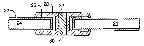
Traversées électriques pratiquées dans des substrats supports (24) de circuits imprimés en vue de la production de plaquettes de circuits imprimés céramiques double face multicouches. Pour réaliser lesdites traversées on isole les ouvertures des traversées au moyen d'une couche d'oxyde de nickel (22) et d'une ou plusieurs couches de verre (26, 28), puis on remplit le volume restant des ouvertures avec une encre (30) métallique conductrice de remplissage. Après cuisson, la structure résultante forme des traversées électriques traversant le substrat support (24).


Abrégé anglais


Electrical feedthroughs in printed circuit board support substrates (24) for
use in making double sided ceramic multilayer printed
circuit boards are made by insulating the feedthrough openings with a first
layer of nickel oxide (22) and one or more layers of glass (26,
28), and then filling the remainder of the feedthroughs with a conductive
metal via fill ink (30). After firing, the resultant structure provides
insulated electrical feedthroughs through the support substrate (24).

Revendications

Note : Les revendications sont présentées dans la langue officielle dans laquelle elles ont été soumises.


7
CLAIMS
1. A fired printed circuit board support substrate made of a metal have a via
that is
lined with a first nickel layer, a second dielectric nickel oxide layer, a
dielectric
glass layer over the nickel oxide layer, the via being filled with a
conductive
material comprising a mixture of conductive metal and a glass, the glass layer
acting to electrically isolate the conductive material from the metal
substrate, the
glass layer having a thermal coefficient of expansion matched to that of the
metal
substrate.
2. The substrate of claim 1 wherein the support substrate is made of a metal
selected from the group consisting of a ferronickel alloy, Kovar, and
composites
of Cu/a ferronickel alloy/Cu, Cu/Mo/Cu and Cu/Kovar/Cu.
3. The substrate of claim 1 wherein the support substrate material comprises a
nickel plated composite selected from the group consisting of
copper/molybdenum/copper, copper/Kovar/copper, copper/a ferronickel
alloy/copper, Invar and Kovar.
4. The substrate of any one of claims 1 to 3 wherein the dielectric glass
layer is
selected from the group consisting of: (a) a glass comprising about 28.68% by
weight of zinc oxide, about 5.92% by weight of magnesium oxide, about 6.21%
by weight of barium oxide, about 15.36% by weight of aluminum oxide and about
43.82% by weight of silicon oxide; and (b) a glass comprising about 29% by
weight of magnesium oxide, about 22% by weight of aluminum oxide, about 45%
be weight of silicon oxide and up to about 4% by weight of oxides of
phosphorus,
boron and zirconium.
5. The substrate of any one of claims 1 to 4 wherein the conductive material
comprises a mixture of conductive metal powder and of a glass that fills the
via.
6. The substrate of claim 5 wherein the glass of the conductive material is
selected
from the group consisting of: (a) a glass comprising about 28.68% by weight of
zinc oxide, about 5.92% by weight of magnesium oxide, about 6.21% by weight

8
of barium oxide, about 15.36% by weight of aluminum oxide and about 43.82%
by weight of silicon oxide; and (b) a glass comprising about 29% by weight of
magnesium oxide, about 22% by weight of aluminum oxide, about 45% by weight
of silicon oxide and up to about 4% by weight of oxides of phosphorus, boron
and
zirconium.
7. The substrate of claim 5 or 6 wherein the conductive metal powder is
selected
from the group consisting of silver, copper and gold.
8. A process for making electrical feedthroughs in a printed board metal
support
substrate for use in making double sided ceramic multiplayer circuit boards
comprising;
a) forming via holes in the substrate;
b) electroplating a nickel lining inside the via holes;
c) forming a nickel oxide layer by oxidizing a surface of the nickel lining;
d) forming an electrically insulating layer by partially filling said via
holes with
a dielectric glass that has a thermal coefficient of expansion matched to
that of the metal support substrate;
e) filling the holes with a thick film of conductor ink of a conductive metal
powder and a glass of paragraph d) in an organic vehicle, and
f) firing the substrate to remove organic materials and to sinter the metal -
and glass (powders) in the via holes.
9. The process of claim 8 wherein the dielectric glass is selected from the
group
consisting of: (a) a glass comprising about 28.68% by weight of zinc oxide,
about
5.92% by weight of magnesium oxide, about 6.21% by weight of barium oxide,
about 15.36% by weight of aluminum oxide and about 43.82% by weight of
silicon oxide; and (b) a glass comprising about 29% by weight of magnesium
oxide, about 22% by weight of aluminum oxide, about 45% by weight of silicon
oxide and up to about 4% by weight of oxides of phosphorus, boron and
zirconium.

9
10. The process of claim 8 or 9 wherein the substrate is selected from the
group
consisting of Invar, Kovar, copper/Kovar/copper composite, copper/ferronickel
alloy/copper composite, and copper/molybdenum/copper composite.
11. The process of any one of claims 8 to 10 wherein the dielectric gas layer
wets
the oxidized nickel lining and can be fired at a temperature up to about
1000°C.

Description

Note : Les descriptions sont présentées dans la langue officielle dans laquelle elles ont été soumises.


CA 02211542 2005-07-04
1
ELECTRICAL FEEDTHROUGHS FOR CERAMIC CIRCUIT BOARD
SUPPORT SUBSTRATES
This invention relates to a method of making electrical feedthroughs
in thermally conductive support substrates used to impart mechanical
strength to ceramic multilayer printed circuit boards. More particularly,
1 0 this invention relates to a method of making electrical feedthroughs in
ceramic multilayer printed circuit board support substrates that is
compatible with mass production techniques.
Ceramic multilayer printed circuit boards have been used for many
years for circuits for electrical apparatus, such as mainframe computers.
1 5 Such printed circuit boards are made by casting glass and/or ceramic
powders together with an organic binder into tapes, called green tapes. A
metal circuit can be patterned onto the green tape by screen printing for
example. Vias are formed in each green tape layer that are filled with a
conductive material to connect the circuits of the various layers
2 0 electrically. The green tape layers are then aligned and stacked, pressed
together, and fired to burn off organic residues and sinter the glass, thereby
forming a fired ceramic multilayer circuit board.
Originally ceramics such as alumina were used to form the green
tape layers, but these ceramics require high firing temperatures, up to
2 5 1500oC. This necessitated the use of refractory conductive metals, such as
tungsten or molybdenum, to form the conductive circuit patterns because
such metals could withstand high firing temperatures without melting.
More recently, lower temperature materials have been used, such as
devitrifying glasses that can be fired at lower temperatures of 1000oC or
3 0 less. Multilayer circuit boards made of these glass or glass-ceramic
materials can be used with lower melting point and higher conductivity
metals, such as silver, gold or copper. However, these printed circuit boards
have the disadvantage that they are not as strong as alumina circuit
boards.
3 5 Thus still more recently, low firing temperature glasses have been
deposited on support substrates made of metal or ceramic to which the
glasses will adhere. The support substrate can be of a thermally
conductive material such as nickel, kovar, a ferrous nickel/

CA 02211542 1997-07-25
w0 96/22881 PCT/US96/00316
2
cobalt/manganese alloy, Invar~, a ferronickel alloy, low carbon steel, or
Cu/kovar/Cu, Cu/Mo/Cu or Cu/Invar~/Cu composites and the like, as well
as thermally conductive ceramics such as aluminum nitride, silicon carbide,
diamond and the like. These substrates impart added strength to the
composite. A bonding glass, such as described in US Patent 5,277,724 to
Prabhu, adheres the ceramic substrate formed from the green tape layers
to the substrate. In addition, if chosen correctly, the bonding glass can
reduce shrinkage of the green tape with respect to the metal substrate in at
least the two lateral dimensions. Thus all of the shrinkage occurs in the
1 0 thickness dimension only. This in turn reduces problems of alignment of
the
circuit patterns in the ceramic layers and the via holes in the metal
substrate after firing.
However, when it is desired to produce glass/ceramic multilayer
ceramic circuit boards on both sides of the support substrate, the presence
1 5 of the thermally and electrically conductive metal or ceramic core
material
between two circuit boards can cause short circuits. Thus the multilayer
circuits on one side of the support substrate have been connected to the
multilayer circuits on the other side of the support substrate by means of
circuit traces or lines that extend around the periphery of the circuit board
2 0 rather than through the support substrate. However, such peripheral
traces are subject to damage or breakage during handling and assembly of
the circuit boards into a module, for example, and in some cases the traces
would have to be too long for an acceptable design. Such designs also
increase wiring lengths and decrease interconnection density. Thus an
2 5 improved method of permitting electrical connection between two ceramic
multilayer circuit boards on both sides of a support substrate would be
highly desirable.
The present process for forming electrical feedthroughs in support
substrates for double sided printed circuit board substrates comprises
3 0 providing dielectric insulation in the feedthroughs. Typically a via hole
is
opened in the support substrate core material, as by drilling, the substrate
via hole is plated with nickel, one or more dielectric materials such as glass
is deposited in the via hole. Lastly a conductive metal is deposited to fill
the
via hole inside the dielectric ring. The dielectric material and the center ,
3 5 conductive metal must be able to withstand several firings at temperatures
up to at least 900oC without melting or flowing.
The teachings of the invention can be readily understood by
considering the following detailed description in conjunction with the

CA 02211542 1997-07-25
WO 96/22881 PCTIUS96I00316
3
accompanying drawing, in which:
Fig. 1 is a flow chart of the preferred process for filling via holes in a
printed circuit board support substrate in accordance with the process of
the invention.
Fig. 2 is a thermal coefficient of expansion plot of a glass suitable for
use as a dielectric in the present process.
Fig. 3 is a differential thermal analysis (DTA) plot of a glass suitable
for use as a dielectric in the present process.
Figs. 4A and 4B illustrate the steps of forming a glass dielectric layer
1 0 in a via hole.
Fig. 5 is a cross sectional partial view of a printed circuit board
support substrate having a filled via hole filled in accordance with the
method of the invention.
The preferred support substrate for use herein is a Cu/Mo/Cu metal
1 5 composite substrate commercially available from the Climax Metals
Company, although other materials can be substituted, as described
hereinabove.
Referring to Fig. 1, which is a flow chart of a suitable process for
making the electrical feedthroughs in a printed circuit board support
2 0 substrate in accordance with the invention, in a first step of the present
process, via openings can be formed in the support substrate using a laser
or mechanical drilling equipment that can drill small diameter holes, e.g.,
about 13-40 mils in diameter or less. The mechanically drilled openings are
then debarred, as by rubbing the edges with a soft stone, whereby via
2 5 openings having sharp corners are eliminated. The thicker the substrate
material, the more difficulty may be encountered in drilling the openings.
Thirteen mil diameter holes can also be readily drilled using a Nd:YAG laser
at 15-30 watts with 0.6 msec pulse lengths. A minimum hole diameter of 7
mils for a 20 mil thick support substrate can be made readily. If the
3 0 thickness of the support substrate is higher, the minimum hole diameter
that can be made may be larger; for example, for a 40 mil thick support
substrate, the minimum hole diameter that can be readily made is 8 mils.
The drilled holes are next debarred and nickel plated. This step seals
the core material of the support substrate and can be accomplished by
3 S conventional nickel electroplating methods. The nickel is then oxidized,
as
by heating in air at temperatures about 820oC. The nickel oxide layer,
which exhibits a resistance of 108 - 109 ohms, constitutes the first ring of
dielectric material in the via hole.

CA 02211542 1997-07-25
WO 96!22881 PCT/US96/00316
4
An insulating dielectric layer, as of a glass, is then deposited in the
via hole to form an annular ring. Since glass is a fragile material that can
crack during multiple firings, it is preferred that two or more layers of
glass
be sequentially deposited in the openings so that if a defect, such as a pore,
forms in one layer, it will not extend through the entire glass layer, to
cause
a shorted feedthrough.
The glasses suitable for use in the present invention, using Cu/Mo/Cu
metal composite substrates, must have a thermal coefficient of expansion
matched to the Cu/Mo/Cu substrate; must have good adhesion to nickel
1 0 oxide, must be able to wet nickel oxide; and must be able to be fired at
temperatures required to form the desired ceramic multilayer circuit board.
One particular glass composition having the following composition in
percent by weight is particularly useful with the above nickel plated
Cu/Mo/Cu composite metal substrate;
1 5 Zn0 28.68
Mg0 5.92
Ba0 6.21
A1203 15.36
Si02 43.82
2 0 This glass has a thermal coefficient of expansion plot as shown in
Fig. 2 and a DTA plot as shown in Fig. 3. This glass can be used as the
dielectric insulator for the substrate via holes. The same glass can also be
used later in the process as a constituent of the thick film conductor via
fill
ink required for filling the center of each via hole with conductive metal, as
2 5 further described below.
Another suitable glass composition for use with the preferred metal
substrate has the following composition in percent by weight:
Mg0 29.0
A1203 22.0
3 0 . Si02 45.0
P205 1.5
B203 1.0
Zr02 1.5
A preferred method of applying the glass composition from a
3 5 standard glazing ink constituting the above glass is to apply vacuum after
the screen printing to deposit one or more of the above glass layers. Such a
glazing ink comprises the finely divided glass and an organic vehicle.
Suitable organic vehicles are solutions of resin binders, such as cellulose

CA 02211542 1997-07-25
WO 96/22881 PCTIUS96100316
derivatives, synthetic resins such as polyacrylates, polymethacrylates,
polyesters, polyolefins and the like, in a suitable solvent. The solvent can
be pine oil, terpineol, butyl carbitol acetate, 2,2,4-trimethyl-1,3-
pentanediol
monoisobutyrate and the like. The vehicles generally contain from about 5
5 to 25 percent by weight of the resin binder.
Thus the glasses of the invention comprise those glasses having a
thermal coefficient of expansion near that of the support substrate
material, will wet nickel oxide and can be fired at a temperature up to about
1000oC. Suitable glasses of the invcention include a glass comprising zinc
1 0 oxide, about 28.68% by weight, magnesium oxide, about 5.92% by weight,
barium oxide, about 6.21% by weight, aluminum oxide, about 15.36% by
weight, and silicon oxide, about 43.82% by weight and a glass comprising
magnesium oxide, about 29% by weight; aluminum oxide, about 22% by
weight, silicon oxide, about 45% by weight and up to about 4% by weight of
1 5 phosphorus oxide, boron oxide and zirconium oxide.
Fig. 4A illustrates a printed glass layer 20 over a via hole 22 in a
metal substrate 24.
A vacuum is applied after the printing, beneath the metal substrate
24 in the direction of the arrow 25, sufficient to bring the glass ink layer
20
2 0 into the via hole 22, thereby forming an annular ring of the glass ink
inside
the via hole 22. This glass layer is then dried. The deposition and vacuum
pull can be repeated to form multiple glass dielectric layers in the via hole
22. If both sides of the metal substrate 24 are to be used, the above
sequence of steps is repeated on the opposite side of the metal substrate
2 5 24.
The support substrate is then fired to sinter the glass powder and
form a composite fired glass insulator layer in the opening.
A thick via fill ink containing a conductive metal powder is then
applied to the metal substrate, also using conventional screen printing
3 0 techniques. For example, a suitable conductor thick film ink comprises a
mixture of silver or other conductive metal powder, glass, and an organic
vehicle as described above in proportions so as to form a print screenable
thick film paste.
Thick film conductor via fill inks are made by mixing a finely divided
3 5 conductive metal powder, with a preselected glass powder and an organic
vehicle. Suitable conductive powders include silver, gold, copper, their
mixtures, and alloys thereof with palladium and platinum and the like, or
nickel. The fired thick film conductive metal ink can comprise from about

CA 02211542 1997-07-25
WO 96/22881 PCT/US96/00316
6
50-90% by weight of metal and about 10-50% by weight of a glass.
The thick film conductor via fill ink composition is applied to the
prepared printed circuit board support substrate so as to fill the glass
insulated via holes and is then fired to remove organic materials and to
S sinter the metal powder to obtain the conductive, insulated feedthroughs.
Fig. 5 is a cross sectional view of the metal substrate 24 having
dielectric insulated electrical feedthroughs therein. The via hole 22 in the
metal substrate 24 has a first layer 22 of nickel oxide dielectric, two
dielectric glass layers 26, 28 and a conductive via fill layer 30 therein.
1 0 Sufficient conductive via fill ink is applied so that the remainder of the
via
hole 22 is completely filled at the end of the process.
The support substrate as prepared above, having conductive vias in
via openings that are dielectrically insulated from the rest of the substrate,
can then be used to prepare double sided multilayer printed circuit boards
1 5 from the substrates of the invention in conventional manner.
The above process can be used to make a reproducible support
substrate having a plurality of electrical feedthroughs therein that will not
form short circuits between circuitry on both sides of the substrate. The
support substrate having electrical feedthroughs as prepared above can
2 0 withstand several firings at temperatures used in making ceramic
multilayer printed circuit boards without undermining the structural and
electrical integrity of the feedthroughs.
Although the present process and electrical feedthroughs have been
described in terms of specific embodiments, one skilled in the art can readily
2 5 substitute other materials and reaction conditions for the glass layers
and
conductors described hereinabove. Thus the scope of the present invention
is only meant to be limited by the appended claims.

Dessin représentatif
Une figure unique qui représente un dessin illustrant l'invention.
États administratifs

2024-08-01 : Dans le cadre de la transition vers les Brevets de nouvelle génération (BNG), la base de données sur les brevets canadiens (BDBC) contient désormais un Historique d'événement plus détaillé, qui reproduit le Journal des événements de notre nouvelle solution interne.

Veuillez noter que les événements débutant par « Inactive : » se réfèrent à des événements qui ne sont plus utilisés dans notre nouvelle solution interne.

Pour une meilleure compréhension de l'état de la demande ou brevet qui figure sur cette page, la rubrique Mise en garde , et les descriptions de Brevet , Historique d'événement , Taxes périodiques et Historique des paiements devraient être consultées.

Historique d'événement

Description Date
Le délai pour l'annulation est expiré 2010-01-29
Lettre envoyée 2009-01-29
Lettre envoyée 2008-04-17
Inactive : Transfert individuel 2008-01-25
Exigences relatives à la révocation de la nomination d'un agent - jugée conforme 2007-06-05
Inactive : Lettre officielle 2007-06-05
Exigences relatives à la nomination d'un agent - jugée conforme 2007-06-05
Demande visant la révocation de la nomination d'un agent 2007-04-26
Demande visant la nomination d'un agent 2007-04-26
Accordé par délivrance 2006-07-04
Inactive : Page couverture publiée 2006-07-03
Préoctroi 2006-04-18
Inactive : Taxe finale reçue 2006-04-18
Inactive : CIB de MCD 2006-03-12
Lettre envoyée 2005-10-18
Un avis d'acceptation est envoyé 2005-10-18
Inactive : CIB attribuée 2005-10-14
Inactive : Approuvée aux fins d'acceptation (AFA) 2005-09-06
Modification reçue - modification volontaire 2005-07-04
Inactive : Dem. de l'examinateur par.30(2) Règles 2005-01-10
Lettre envoyée 2003-01-09
Requête d'examen reçue 2002-12-04
Exigences pour une requête d'examen - jugée conforme 2002-12-04
Toutes les exigences pour l'examen - jugée conforme 2002-12-04
Inactive : Transfert individuel 1997-11-17
Inactive : CIB attribuée 1997-10-22
Symbole de classement modifié 1997-10-22
Inactive : CIB en 1re position 1997-10-22
Inactive : Lettre de courtoisie - Preuve 1997-10-14
Inactive : Notice - Entrée phase nat. - Pas de RE 1997-10-07
Demande reçue - PCT 1997-10-03
Demande publiée (accessible au public) 1996-08-01

Historique d'abandonnement

Il n'y a pas d'historique d'abandonnement

Taxes périodiques

Le dernier paiement a été reçu le 2006-01-03

Avis : Si le paiement en totalité n'a pas été reçu au plus tard à la date indiquée, une taxe supplémentaire peut être imposée, soit une des taxes suivantes :

  • taxe de rétablissement ;
  • taxe pour paiement en souffrance ; ou
  • taxe additionnelle pour le renversement d'une péremption réputée.

Les taxes sur les brevets sont ajustées au 1er janvier de chaque année. Les montants ci-dessus sont les montants actuels s'ils sont reçus au plus tard le 31 décembre de l'année en cours.
Veuillez vous référer à la page web des taxes sur les brevets de l'OPIC pour voir tous les montants actuels des taxes.

Titulaires au dossier

Les titulaires actuels et antérieures au dossier sont affichés en ordre alphabétique.

Titulaires actuels au dossier
LAMINA LIGHTING, INC.
Titulaires antérieures au dossier
ANANDA HOSAKERE KUMAR
BARRY JAY THALER
EDWARD JAMES CONLON
THOMAS PETER AZZARO
Les propriétaires antérieurs qui ne figurent pas dans la liste des « Propriétaires au dossier » apparaîtront dans d'autres documents au dossier.
Documents

Pour visionner les fichiers sélectionnés, entrer le code reCAPTCHA :


Pour visualiser une image, cliquer sur un lien dans la colonne description du document. Pour télécharger l'image (les images), cliquer l'une ou plusieurs cases à cocher dans la première colonne et ensuite cliquer sur le bouton "Télécharger sélection en format PDF (archive Zip)" ou le bouton "Télécharger sélection (en un fichier PDF fusionné)".

Liste des documents de brevet publiés et non publiés sur la BDBC .

Si vous avez des difficultés à accéder au contenu, veuillez communiquer avec le Centre de services à la clientèle au 1-866-997-1936, ou envoyer un courriel au Centre de service à la clientèle de l'OPIC.


Description du
Document 
Date
(aaaa-mm-jj) 
Nombre de pages   Taille de l'image (Ko) 
Dessin représentatif 1997-10-30 1 4
Revendications 1997-07-24 2 107
Dessins 1997-07-24 2 39
Abrégé 1997-07-24 1 46
Description 1997-07-24 6 369
Revendications 2005-07-03 3 108
Description 2005-07-03 6 368
Dessin représentatif 2006-06-01 1 7
Rappel de taxe de maintien due 1997-10-06 1 111
Avis d'entree dans la phase nationale 1997-10-06 1 193
Courtoisie - Certificat d'enregistrement (document(s) connexe(s)) 1998-03-24 1 118
Rappel - requête d'examen 2002-09-30 1 116
Accusé de réception de la requête d'examen 2003-01-08 1 174
Avis du commissaire - Demande jugée acceptable 2005-10-17 1 161
Courtoisie - Certificat d'enregistrement (document(s) connexe(s)) 2008-04-16 1 105
Avis concernant la taxe de maintien 2009-03-11 1 171
PCT 1997-07-24 6 223
Correspondance 1997-10-13 1 36
PCT 1997-07-27 1 46
Correspondance 2006-04-17 1 45
Taxes 2007-01-14 1 31
Correspondance 2007-04-25 3 69
Correspondance 2007-06-04 1 13
Correspondance 2007-06-04 1 16