Note : Les descriptions sont présentées dans la langue officielle dans laquelle elles ont été soumises.
CA 02213426 1997-08-18
96P5533 -1- PATENT APPLICATION
CIRCUIT ARRANGEMENT FOR OPERATING ELECTRICAL
INCANDESCENT BULBS
BACKGROUND OF THE INVENTION
The invention concerns circuit arrangements for
operating electrical incandescent bulbs, particularly
low-volt halogen incandescent bulbs.
This type of circuit arrangement contains as
principal component a self-starting current-feedback
inverter iri half-bridge circuit, which chops the low-
frequency mains voltage or d.c. voltage of the
electrical supply into a high-frequency voltage. This
voltage is then transformed by means of a power
transformer to the low voltage of the halogen
incandescent bulbs that are used, for example, usually
to 6, 12 or 24 V. Such circuit arrangements are thus
called electronic transformers or electronic
converters. A detailed explanation of the functioning
of electronic converters is disclosed, for example, in
EP Patent 264,765 and DE-OS (Unexamined) 4,011,742.
A protective device is indispensable in order to
prevent self-destruction of the circuit arrangement
with a possible danger of fire as well as endangering
of persons when, an overload or short circuit occurs,
i.e., when an inadmissible low-ohm load arises, for
example, caused by parallel connection of several
CA 02213426 1997-08-18
96P5533 -2- PATENT APPLICATION
bulbs or by short circuiting of the bulb leads. For
this purpose, a detector circuit is necessary, which
supplies a suitable detection signal in the case of
overload or short circuit. For brevity, this circuit
will be called the overload detector circuit in the
following. The detection signal then serves as the
control signal for a cutoff circuit, which disconnects
the electronic converter at least temporarily.
After disconnection, the high-frequency
oscillation of the inverter must be initiated again.
Commonly, electronic converters contain a starting or
triggering generator, which assumes this task. The
electronic converter must be separated for a short
time from the supply voltage. After a repeated
application of the supply voltage, the inverter again
oscillates.
A self-oscillating inverter in half-bridge
circuit for a low-volt lamp with a protection circuit
and a current measurement member is known from
DE 42 42 120 A1. The current measurement member
comprises essentially four resistors and a zener diode
which is connected between the source of the lower
half-bridge field effect transistor and the reference
potential. A disadvantage of this solution is that
the currrent measuring member requires a relatively
large number of components. Also, the signal tapped
from the resistance circuit for controlling the
protective circuit is approximately proportional to
the lamp current. In order to be able to distinguish
at all between normal case and overload case, the
CA 02213426 2004-03-30
-3-
protective circuit must be configured to have a very steep flank.
EP 0 647,084 A1 discloses a circuit arrangement with a self starting half
bridge transformer
and a detector circuit. The detector circuit comprises a serial connection of
a diode and a resistance,
which is connected in parallel to the bridge capacitor connected to ground
potential. In addition,
the bridge capacitors and the power transformer are dimensioned in such a way
that the diode is
conductive only when overload occurs. The serial resistance then transforms
the current flowing
through the diode into a voltage signal, which serves as a detection signal
and controls a cutoff
circuit. A disadvantage of this solution is the fact that the dimensioning of
the half bridge
transformer must be fine-tuned to the detector circuit.
SUMMARY OF THE INVENTION
The task of the invention is to avoid this disadvantage and to provide a
circuit arrangement,
which reliably produces a detection signal, which controls a cutoff circuit,
in the case of overload
or short circuit, and which has as few components as possible and is thus cost-
favorable.
In one aspect, there is provided circuit arrangements for operating electrical
incandescent
bulbs, particularly low-volt halogen incandescent bulbs, on an alternating-
voltage network or a d.c.
voltage source with a self oscillating half bridge inverter having two
controllable half bridge
switches and feedback by means of a control transformer, two half bridge
capacitors each having
a first side connected at a connection point, a power transformer, whose
primary winding is coupled
on one side to control transformer and on the other side is contacted with
connection point of the
two half bridge capacitors and incandescent bulbs) is (are) connected to its
secondary winding, an
overload detector circuit, a cutoff circuit connected to overload detector
circuit, which disconnects
the half bridge inverter at least temporarily in the case of overload or short
circuit, is hereby
characterized in that the overload detector circuit is serially connected
between a first capacitor of
the two half bridge capacitors and a reference potential of the half bridge
inverter, and that the
CA 02213426 2004-03-30
-4-
connection point between first half=bridge capacitor and overload detector
circuit is connected with
cutoff circuit.
The invention provides for specifically connecting an impedance operating as a
current-
voltage transformer, for example, a resistance, in series with a bridge
capacitor. In this way, it is
achieved that the charging or discharging current of the corresponding bridge
capacitor flows
through the current-voltage transformer in the oscillation cycle of the half
bridge transformer. The
current-voltage transformer transforms this current signal into a voltage
signal. This voltage signal
is used for controlling a cutoff circuit. For this purpose, the current-
voltage transformer is
connected to the cutoff circuit of the electronic converter. By suitable
dimensioning of the current-
voltage transformer, the cutoff circuit will disconnect the inverter at least
temporarily in the case
of overload or short circuit.
In a simple embodiment, a resistance is connected between the first bridge
capacitor
connected to the reference potential, e.g., the minus pole of the inverter,
and the reference potential.
In this way, a voltage signal proportional to the load current through this
first bridge capacitor can
be tapped between the reference potential and the connection point of the
first bridge capacitor and
resistance, and this voltage signal is used as the detection signal. For this
purpose, the connection
point is contacted with the cutoff circuit. This solution is particularly cost-
favorable, since the
detector circuit only requires an additional resistance.
The value of the resistance may lie in the range between approximately 0.1 S2
and 10 SZ,
preferably in the range between approximately 0.3 SZ and 3 S2. With respect to
a particularly
compact circuit arrangement,
CA 02213426 1997-08-18
96P5533 -5- PATENT APPLICATION
the resistance is preferably executed by SMD (Surface
Mounted Device) technology.
In an advantageous embodiment of an inverter with
bipolar switching transistors, the current-voltage
transformer is a component of the base circuit of one
of the switching transistors, particularly of the
switching transistor connected to the reference
potential (ground). Preferably, the current-voltage
transformer is the resistance in the serial circuit of
resistance and choke connected in parallel to the
base-emitter path, which has been disclosed in DE OS
(Unexamined) 4,436,465. According to the instructions
of DE OS 4,436,465, the connection point between the
resistance and the choke is connected with the foot
point of the bridge capacitor that is otherwise
usually connected directly with the reference
potential. This arrangement opposes a decrease of the
operating frequency of the transformer in the upper
nominal load range. The efficiently useful range of
the power connection can be expanded in this way. The
present invention now utilizes this resistance also as
the current-voltage transformer for producing the
detection signal. For this purpose, the connection
point between resistance and choke is contacted with
the cutoff circuit. This solution is particularly
cost-favorable for electronic converters with a large
nominal load range, for which the frequency adaptation
circuit of DE-OS (unexamined) 4,436,465 is also
provided. In this case, no additional electronic
component is necessary for the detector circuit. Only
CA 02213426 2004-03-30
-6-
an additional contacting between the connection point of the resistance and
choke, on the one hand,
and the cutoff circuit, on the other hand, must be produced.
The inductivity value of the choke may lie in the range between approximately
1 ~,H and
100 gH, particularly in the range between approximately 10 ~,H and 30 g,H. For
a particularly
compact circuit arrangement, the choke is preferably executed as a bar choke.
The cutoff circuit may contain a cutoff component, for example, a switching
transistor or
a thyristor, and usually a signal-conditioning circuit for processing the
detection signal. The
electronic converter is disconnected, for example, by short-circuiting the
control connection of a
switch of the inverter or of the trigger generator by means of the cutoff
element, as disclosed, e.g.,
in EP 0 647,084 Al.
BRIEF DESCRIPTION OF THE DRAWINGS
The invention will be explained in more detail on the basis of the following
examples of
embodiment.
Here:
Figure 1 shows a principle circuit diagram of an electronic converter with an
overload
detector circuit for the onerati~n ~f lnw-volt halnuPn inranr~PCrPnt h"lhe~
CA 02213426 1997-08-18
96P5533 -7- PATENT APPLICATION
Figure 2 shows a principle circuit diagram as in
Figure 1, but also with a frequency adaptation
circuit;
Figure 3 shows an electrical circuit diagram of
an electronic converter with an overload detector or
protection circuit and with a frequency adaptation
circuit for operating low-volt halogen incandescent
bulbs.
BEST MODE FOR CARRYING OUT THE INVENTION
Figure 1 shows a principle circuit diagram of an
electronic converter according to the invention with
an overload detector circuit for operating low-volt
halogen incandescent bulbs HG. The converter is
comprised of a half-bridge transformer, which is fed
by supply voltage U and has two controllable bridge
switches S1, S2, and two bridge capacitors C1, C2, a
feedback and control circuit RSK for maintaining the
high-frequency oscillation of the half-bridge
transformer, which selectively controls bridge
switches S1, S2, and if needed, it also may contain a
trigger generator (not explicitly shown) for re-
oscillation of the half-bridge transformer, a power
transformer LU, which is fed by the half-bridge
transformer, and is connected on one side with a low-
volt halogen incandescent bulb HG and on the other
side is connected to feedback and control circuit RSK,
a current-voltage transformer SSW, which represents
the detector circuit itself and is connected in series
CA 02213426 1997-08-18
96P5533 -8- PATENT APPLICATION
to a bridge capacitor C1, and a cutoff circuit AK,
whose input is connected to current-voltage
transformer SSW and whose output is connected to
feedback and control circuit RSK. The current-voltage
transformer SSW produces a voltage signal, which
controls cutoff circuit AK. In case of overload or
short circuit, cutoff circuit AK operates directly on
feedback and control circuit RSK such that it
interrupts the oscillation of the half-bridge
transformer.
Figure 2 also shows a principle circuit diagram
of an electronic converter according to the invention.
In contrast to Figure 1, this variant also contains a
frequency adaptation circuit (not shown explicitly),
which is completed by the current-voltage transformer
of the detector circuit to form a frequency adaptation
and detector circuit FDK. Frequency adaptation and
detector circuit FDK is connected on one side with the
control connection of a bridge switch S1 and opposes a
decrease of the transformer frequency in the upper
range of the power connection. On the other side,
frequency adaptation and detector circuit FDK is
connected to cutoff circuit AK and, corresponding to
the functioning described in Figure 1, causes an
interruption of the oscillation of the half-bridge
transformer in the case of overload or short circuit.
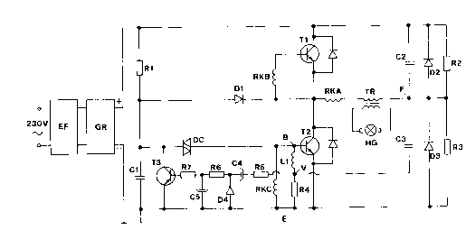
Figure 3 shows an electrical circuit diagram of
an electronic converter according to the invention for
operating low-volt halogen incandescent bulbs. The
circuit arrangement contains, among other components,
CA 02213426 1997-08-18
96P5533 -9- PATENT APPLICATION
an overload detector circuit or an overload cutoff
circuit as well as a frequency adaptation circuit and
has the following features: an input filter (EF) for
suppressing counter-cycle interference currents, a
rectifier GR, whose minus pole is connected to the
ground potential of the circuit, and is the reference
potential in the following, a trigger generator,
comprised of resistance R1, charging capacitor C1 and
diac DC, a self-starting feedback half-bridge
transformer--it essentially comprises two half-bridge
transistors, T1, T2, half-bridge capacitor C2 and
control transformer RKA-RKC for feedback--, a power
transformer TR, at the secondary winding of which is
operated a low-volt halogen incandescent bulb HG, a
frequency adaptation circuit comprised of a serial
connection of choke L1 and resistance R4 as well as
branch capacitor C3, an overload detector circuit
comprised of resistance R4 of the frequency adaptation
circuit, which operates here in its second function as
a current-voltage transformer for producing the
detection signal, as well as a cutoff circuit with
upstream-connected signal-conditioning circuit,
comprised of an inverter circuit with resistance R5,
capacitor C4 and diode D4, a retarding and holding
component comprised of capacitors C4, C5 and the two
resistances R6 and R7 as well as a cutoff transistor
T3. A detailed explanation of the functioning of the
signal-conditioning circuit or of the cutoff circuit
is found in EP 0 647,084 A1.
CA 02213426 1997-08-18
96P5533 -10- PATENT APPLICATION
In one variant, instead of the negative
components, the positive components of the detection
signal are used for control of the cutoff circuit. In
this case, the signal-conditioning circuit does not
contain an inverter circuit.
Branch capacitor C3 is contacted with the
connection point V between choke L1 and resistance R4
on one side as well as foot point F of half-bridge
capacitor C2 connected with the plus pole of the
rectifier on the other side, and acts simultaneously
as the second half-bridge capacitor. The connection
of the serial circuit on the choke side is connected
at point B with the base and the terminal on the
resistance side is connected at point E with the
emitter of half-bridge transistor T2 contacted by
ground potential. A detailed explanation of the
functioning of the frequency adaptation circuit is
found in DE OS (unexamined) 4,436,465.
The design of the input filters is described,
e.g., in H.J. Meyer, "Current supplies for practice",
Vogel Book Publishers Wiirzburg, 1989, pages 115-116
(in German). The rectifier GR essentially comprises a
diode full bridge (see e.g., W. Hirschmann and A.
Hauenstein, "Switched-Mode Power Supplies", Siemens AG,
1990, p. 102 (in German)) and transforms the
alternating voltage of the mains into a pulsating d.c.
voltage +UH .