Note : Les descriptions sont présentées dans la langue officielle dans laquelle elles ont été soumises.
CA 02213436 1997-08-20
W ~96/26627 PCTnUS96)~D17
THOD FOR MU~UFACTURING
ELECTROLUMINESCENT LAMPS
BACKGROUIID OF THE IN~ENTION
1. Field of the Invention
The present invention relates to electroluminescent lamps, and more
particularly to a method for ma:~ufacturing water proof
electroluminescent lamps which are sl1itable for many low-cost
consumer applications.
2. DescriPtion of the Prior Art
Conventional electroluminescent (EL) lamp manufacturing techniques
may be divided into two basic processes. The first is a screen
printing process in which the lamp is constructed layer by layer.
More particularly, the lamp is constructed using costly
electroluminescent inks, clear conducti.ve indium t:in oxide (ITO)
transparent films, conductive inks compounded with a high volume of
metallic silver and a water repellent electrical in~lulating coating
cont~;n;ng an ultraviolet light-activated polymer.
The screen printing process allows intricate graphics effects to be
created using relatively simple manufacturing processes. However,
screen printed EL lamps having high luminance or superior electrical
characteristics tend to be costly to manufacture. Typical
manufacturing costs in high volume applications range from eight to
thirteen cents per square inch, while m;n;m~l quality and performance
st~n~rds result in savings of less than t:wo cents per square inch.
The second process is the continuous lamination method. In this
process, a first film which supports a foil is passed below a
metering roller or blade which applies an insulating layer of ink. A
~ second transparent film that has been sputter coated with clear
conductive ITO is similarly passed below a roller or blade, which
CA 02213436 1997-OX-20
W 096/26627 PCT/u~96r~l76
applies a layer of phosphor ink. In order to achieve a uniform light
output and electrical characteristics, the thickness of the
insulating and phosphor layers must be precisely controlled, along
with the phosphor grain dispersion in the phosphor layer. Thus, the
continuous lamination method requires very tight control over ink
rheology.
Once the ink layers have been dried and inspected for defective
areas, the first and second films are laminated together to form a
lamp core. The film lamination requires heat and/or pressure which
must be tightly controlled so that the light and electrical
characteristics of the finished lamp are not affected. Additionally,
since the phosphor layer is sensitive to water contamination, the
finished lamp is cut into the desired size and shape, electrically
t~rm;n~ted and encapsulated within a water impervious lamination film
(such as Allied Signal's "ACLAR" CTFE).
The continuous lamination method produces foil EL lamps, which are
high performance, high priced lamps typically unsuitable for graphics
or other price-sensitive applications. Foil EL lamps are also
thicker and mechanically less flexible than screen printed EL lamps.
The typical cost of foil sensitive lamps is greater than thirty cents
per square inch, and the lamps are typically used in military,
aircraft and high-end industrial applications.
Accordingly, there is a need for a method for manufacturing low-cost
EL lamps which can be applied to both graphics and price-
sensitive consumer applications.
CA 02213436 1997-08-20
W O 96/26627 l~CTMS96)0~176
SUMM~RY OF THE INVENTION
The present invention is directed to a method for manufacturing EL
lamps which incorporates some of the processes which have been used
in manu~acturing flexible printed circuit boards.
In an exemplary embodiment of the invention, the method of the
present invention includes the following steps. In the first step, a
metal foil is bonded to an insulating paper or plastic core stock and
is die cut or chemically etched to form one or more rear capacitive
electrodes. Next, the insulating paper or plastir core stock is
coupled to a precisely positioned indexing system. In the preferred
embodiment, the indexing system may include sprocket holes along one
or more edges of the insulating paper or plastic core stock.
In the third step, a layer of hygrophobically compounded high
dielectric strength EL phosphor ink is applied to the rear capacitive
electrodes to precisely form the areas of illumination. The EL
phosphor ink is allowed to bleed past the edges of the rear
capacitive electrodes, thereby providing insulation between the front
and rear capacitive electrodes. In step ~our, a layer of transparent
or translucent conductive indium tin oxicle (ITO) or tin oxide ink is
applied to cover the layer of EL phosphor ink, ~-orming a front
capacitive electrode. The ITO ink is al]owed to bleed beyond the EL
phosphor ink in order to make contact: with a metal foil power
conductor.
Next, in step five a transparent polyester film or ultraviolet
activated dielectric coating is applied t:o the entire surface of the
lamp. Finally, in step six metal foil power conductors are provided
to the front and rear capacitive electrodes.
A first embodiment of an EL lamp manufactured by the method of the
present invention comprises a capacitive electrode bonded to a paper
core stock. A layer of EL phosphor ink is printed on the capacitive
electrode to precisely define the areas of illumination. A layer of
conductive ITO ink printed on the EL phosphor layer and is covered by
an insulating layer consisting of a transparent polyester film.
CA 02213436 1997-08-20
W 096/26627 PCTAUS96/00176
In a second embodiment of an EL lamp manufactured by the method of
the present invention, the capacitive electrodes and phosphor ink and
ITO layers are bonded to both surfaces of the paper core stock. The
embodiment provides a low-cost EL lamp which emits light from both
surfaces.
The method of the present invention provides the ability to t
manufacture EL lamps at a cost of less than five cents per square
inch. Additionally, these low-cost EL lamps can be manufactured
using existing or readily obt~;n~hle equipment.
Further features and advantages of the present invention will be
appreciated by a review of the following detailed description of the
preferred embodiments taken in conjunction with the following
drawings.
CA 02213436 1997-08-20
W O 96/26627 PCTnUS96J~D276
BRIEF DESCRIPTION OF THE DRAWINGS
The present invention may be best unde:rstood by referring to the
following detailed description of the preferred embodiments and the
accompanying drawings, wherein like numerals denote l:ike elements and
in which:
Figs. l(a)-(d) are a sequence o~ diagram, illustrating a method for
manufacturing a low-cost EL lamp in accordance with the present
invention;
Fig. 2 is a cross-sectional view of a first exemplary EL lamp 100
constructed in accordance with the method o~ Figs. l(a)-(d);
Fig. 3 is a top view of EL lamp 100 of Fiq. 2;
Fig. 4 is a schematic diagram of an equivalent circ:uit of EL lamp
100;
Fig. 5 is a cross-sectional view of a second exemplary EL lamp 200
constructed in accordance with the method of Figs. l(a)-(d);
Fig. 6 is a top view of EL lamp 200 of Fig. 5; and
Fig. 7 is a schematic diagram of an equ:ivalent circuit of EL lamp
200.
-
CA 02213436 1997-08-20
W 096/26627 PCTrUS96/00176
DETAILED DESCRIPTION OF THE PREFERRED EMBODIMENTS
The following exemplary discussion focuses on the manufacturing of a
low-cost electroluminescent (EL) lamp. The (EL) lamp produced by the
method of the present invention is suitable for a variety of graphics
and low-cost consumer applications.
Referring to Figs. l(a)-(d), a se~uence of diagrams illustrating a
preferred method for manufacturing a low-cost EL lamp in accordance
with the present invention is shown. In the first step of the
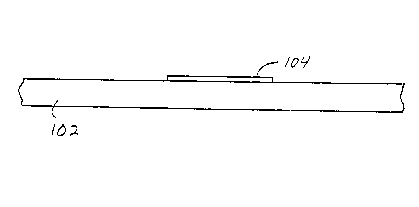
method, a 0.002 inch thick metal foil is die cut or chemically etched
to form one or more rear capacitive electrodes 104 which are bonded
to a paper or plastic core stock 102. Alternatively, the metal foil
can also be embossed onto the paper or plastic core stock from a
separate metal foil supply. The typical thickness of paper or plastic
core stock 102 is approximately 0.01 inch. The die cutting or
chemical etching may be done using any of a number of conventional
techniques. Additionally, paper or plastic core stock 102 may be
coupled to a conventional precision indexing system (not shown),
which may use sprocket holes which are provided along one or more
edges of paper or plastic core stock 102.
In the next step, a layer of EL phosphor ink 106 is applied to rear
capacitive electrodes 104 to precisely form the areas of
illumination. EL phosphor ink layer 106 is allowed to bleed past the
edges of rear capacitive electrodes 104 by approximately 0.02 inch,
thereby insulating rear capacitive electrodes 104. A layer of
conductive ITO ink 108 is then applied to cover layer of EL phosphor
ink 106, with ITO ink layer 108 also being allowed to bleed past the
edges of EL phosphor ink layer 106 by approximately 0.02 inch. The
use of the precision indexing system allows the distribution of the
layers of EL phosphor ink 106 and conductive ITO ink to be
specifically limited to those areas of capacitive electrodes 104
which are to be illuminated. For example, complex graphical patterns
such as circles within circles, text or individually addressable lamp
elements (pixels) may be created.
CA 02213436 1997-08-20
W O 96/26627 PCTnUS96~0017~
Continuing with Figs. l(a)-(d), a transparent or translucent
polyester film 110 is then applied to the entire surface of the lamp.
Polyester film 110 is typically 0.0005 inch thick, which provides
adequate protection against cont~m;n~tion and possible electrical
shock.
In an alternative ~irst step, the metal foil may be replaced by a
conductive plastic film which has been die cut to form capacitive
electrodes 104. In addition, EL phosphor ink 106 ma~ be replaced by
a plastic film imbued with EL phosphors. Similarly, conductive ITO
ink 108 may be replaced by an ITO-coated transparen~ or translucent
polyester film. Further, transparent or translucent polyester film
110 may be replaced by an ultraviolet activated dielectric coating.
Paper or plastic core stock 102 may be replaced with any of a variety
of flexible, non-conducting materials such as thin plastic or
fiberglass. Further, paper or plastic core stock 102 may be
completely replaced by a metal foil which has been coated on one or
both surfaces by layers of EL phosphor ink, a conductive ITO coating
and a transparent or translucent insulati:ng coating or lamination.
Referring now to Fig. 2, a cross-sectional view of a first exemplary
EL lamp 100 constructed in accordance with the above method is shown.
Lamp 100 includes paper or plastic core stock 102, rear capacitive
electrode 104, EL phosphor layer 106, front conductive ITO layer 108
and clear electrical insulator 110. Note that layers 106 and 108
both overlap rear capacitive electrode 104 in order to provide
electrical isolation between layers 106 a:nd 108, while allowing layer
108 to make contact with a metal foil power conductor. Capacitive
electrode 104 is permanently bonded to paper core st.ock 102 using a
non-conducting bonding compound. EL phosphor layer 106 provides a
precise definition of the area of illumination, while avoiding any
waste of the expensive phosphor ink.
Fig. 3 provides a top view of exemplary EL lamp 100. As shown in
Fig. 3, capacitive electrode 104 and EL phosphor ink layer 106 define
a rectangular area of illumination. However, the specific shape of
the area of illumination is not limited to simple rectangles, circles
or polygons. Any pattern with which EL phosphor ink may be printed
onto capacitive electrode 104 may define l_he area of .illumination.
CA 02213436 1997-08-20
W 096/26627 PCTrUS96/00176
Continuing with Fig. 3, metal foil conductors 112 and 114 are used to
provide electrical power to rear capacitive electrode 104 and front
conductive ITO layer 108. When an appropriate alternating current
(AC) power source is connected to conductors 112 and 114, current
flows through EL phosphor ink 106, thus providing illumination. Note
also that the mechanical structure of EL lamp 100 provides a lighting t~
source which is light-weight and flexible.
Referring now to Fig. 4, a schematic diagram of an equivalent
electrical circuit of EL lamp 100 is shown. EL lamp 100 functions as
a capacitor with capacitive electrode 104 as one plate and conductive
ITO layer as the other plate. EL phosphor ink layer 106 form the
dielectric of the capacitor. When an AC power source is connected to
terminals 112 and 114, current passes through phosphor ink layer 106
resulting in illumination.
Referring now to Fig. 5, a cross-sectional view of a second exemplary
EL lamp 200 constructed in accordance with the above method is shown.
Lamp 200 includes paper or plastic core stock 202, rear capacitive
electrode 204, EL phosphor layers 208 and 210, front conductive ITO
layers 212 and 214 and clear electrical insulator 216. Rear
capacitive electrode 204 is permanently bonded to paper or plastic
core stock 202 using a non-conducting bonding compound. EL phosphor
layers 208 and 210 provide a precise definition of the area of
illumination, while avoiding any waste of the expensive phosphor ink.
Fig. 6 provides a top view of exemplary EL lamp 200. As shown in
Fig. 6, rear capacitive electrode 204 and EL phosphor ink layers 208
and 210 define a pair of rectangular areas of illumination. However,
the specific shape of the areas of illumination is not limited to
simple rectangles, circles or polygons. Any patterns with which EL
phosphor ink may be printed onto capacitive electrode 204 may define
the area of illumination.
Continuing with Fig. 6, metal foil conductors 206, 218 and 220 are
used to provide electrical power to capacitive electrode 204 and
conductive ITO layers 212 and 214. When an appropriate AC power
source is connected to conductors 206 and 218, current flows through
EL phosphor ink layer 210 to ITO layer 212, thus providing
illumination of the corresponding rectangular area. Similarly, when
-
CA 02213436 1997-08-20
WO 96/26627 ]PCTrUS96JOD~7~
an AC power source is connected to conductors 206 and 220, current
flows through EL phosphor ink layer 208 to ITO :Layer 214, thus
providing illumination of the corresponding rectangular area.
Finally, when an AC power source is connected to co~lductors 218 and
220, current flows through EL phosphor ink layers 2()8 and 210 using
rear capacitive electrode 204 as a capacitive current path, thus
providing illumination of both rectangular areas. Therefore, either
or both rectangular areas may be illuminated by providing power to
the appropriate electrical terminals.
Note also that the mechanical structure of EL lamp 100 provides a
lighting source which is light-weight and flexible.
Referring now to Fig. 7, a schematic diagram of an equivalent
electrical circuit of EL lamp 200 is shown. EL lamp 200 functions as
a pair of capacitors connected in series, with capacitive electrode
204 as the center plate and conductive ITO layers 21:2 and 214 as the
outer plates. EL phosphor ink layers 208 and 210 form the dielectric
regions of the capacitors. When an AC power source is connected to
terminals 206 and 220, current passes through phosphor ink layer 208
resulting in illumination. Similarly, when an AC power source is
connected to terminals 206 and 218, current passes t;hrough phosphor
ink layer 210 resulting in illuminationO Finally, when an AC power
source is connected to terml n~l S 218 and 220, current passes through
phosphor ink layers 208 and 210 resulting in illumination.
Thus, the method of present invention provides a low-cost EL lamp
which provides substantial illumination. Additiona]ly, the EL lamp
produced by the method of the present inv~ention consume low power and
generate little or no heat. Further, the EL lamp produced by the
method of the present invention has an essentially ~mlimited useful
life, making regular replacement unnecessary.
The foregoing description includes what are at present considered to
be preferred embodiments of the invention. However, it will be
readily apparent to those skilled in the art that various changes and
modifications may be made to the embodiments without departing from
the spirit and scope of the invention. Accordingly, it is intended
that such changes and modifications fall within the spirit and scope
of the invention, and that the invention be limited only by the
CA 02213436 1997-08-20
W 096/26627 PCTrUS96/00176
following claims.
1 0