Note : Les descriptions sont présentées dans la langue officielle dans laquelle elles ont été soumises.
CA 02213619 1997-08-22
TECHNICAL FIELD
The present invention relates generally to wireless modems, and more
particularly to a method for utilizing the communications protocol and
hardware of a
radio frequency identification (RFID) transponder system as a low-cost,
miniature
wireless modem.
BACKGROUND OF THE INVENTION
Microprocessors and their associated memory are used to improve the
operation, usability, and control of many electronic and electro-mechanical
products.
Typically, the memory of these products includes non-volatile memory that
advantageously preserves important system data when the power supply to the
product
is turned off, disconnected, or otherwise rendered inoperative. Such system
data may
include default configuration data required during startup of the
microprocessor or
diagnostic data that facilitates the identification of operational problems.
As the use of microprocessors and associated memory in electronic and electro-
mechanical products proliferates, there is an increasing need to access system
data
stored in the non-volatile memory for diagnostic and/or data modification
purposes. For
example, if a product becomes inoperable, it is generally desirable to access
system
data stored in the memory to search for data errors. If an error is found in
the system
data, it is necessary to correct the system data stored in the memory, thereby
restoring
the product to proper operation.
Access to the memory oftentimes requires costly diagnostic devices that are
connectable to the memory of the product via direct electrical contact
therewith.
Although some diagnostic devices are connectable to the memory of the product
via
indirect electrical contact, such as via a user interface integral with the
product, these
devices have limited utility because they are generally only applicable if the
user
interface, and correspondingly the product, is functioning properly.
Diagnostic devices
that are connectable to the memory of a product via direct electrical contact
are also
problematic in cases where the memory resides in a relatively inaccessible
location
within the product, rendering direct electrical contact between the diagnostic
device and
the memory extremely difficult. In such cases, it may be necessary for a
technician to
1
CA 02213619 1997-08-22
disassemble the product before the memory is accessible, which requires a
significant
amount of time and substantially increases the cost of servicing the product.
There are other cases where it is not practical to access the non-volatile
memory
of a microprocessor via direct or indirect electrical contact, such as in the
case of a field
replaceable unit (FRU) for a computer. An exemplary FRU is a computer circuit
board
having a microprocessor and an associated non-volatile memory, wherein the
memory
is powered by a battery when the memory is disconnected from its external
power
source. The non-volatile memory usually contains important system data read by
the
computer during startup and/or operation of the computer. It is sometimes
necessary
to read the system data stored in the non-volatile memory of the FRU or to
correct,
update, or replace the system data stored therein, particularly when the
computer is
shut off, malfunctioning or otherwise inoperable. Yet the contents of the non-
volatile
memory are not readily accessible by indirect electrical contact under these
conditions
because the user interface of the computer is often correspondingly
inoperable. Thus,
the computer must be disassembled to access the memory via direct electrical
contact.
Disassembly, however, is an unsatisfactory alternative, as noted above, due to
the high
costs associated therewith.
Still another alternative is to access the non-volatile memory using a
conventional contactless communication device such as a wireless modem.
Wireless
modems are used to transfer data between remote locations without requiring
electrical
contact therebetween. Conventional wireless modems, however, have a relatively
high
cost that prevents or discourages their use in low-cost products. Conventional
wireless
modems are also too large for use in products where miniaturization is
required.
Accordingly, it is an object of the present invention to provide a wireless
modem
that allows communication with the memory of an electrical or electro-
mechanical host
device without requiring connection therebetween by either direct or indirect
electrical
contact. It is another object of the present invention to provide a wireless
modem that
is small in size. It is yet another object of the present invention to provide
a wireless
modem that is relatively low in cost. These objects and others are achieved by
the
present invention described hereafter.
2
CA 02213619 1997-08-22
SUMMARY OF THE INVENTION
The present invention is a method for remotely accessing a memory of an
electrical or electro-mechanical device by means free of direct or indirect
electrical
contact with the device memory. In accordance with the method, a remote
exciter/reader is provided that is free of electrical contact with the memory
of the
electrical or electro-mechanical device. A transponder is also provided,
including an
antenna, a reading circuit, and a transponder memory. The transponder memory
is in
direct electrical contact with the device memory.
The method is initiated by generating a radio frequency (RF) excitation signal
using the exciter/reader and transmitting the RF excitation signal to the
transponder.
The RF excitation signal powers the transponder, causing the reading circuit
of the
transponder to generate an RF response signal that includes data from the
device
memory. The RF response signal is transmitted via the antenna back to the
exciter/reader where the RF response signal is read.
In another aspect of the invention, the exciter/reader includes a writer that
generates an RF write signal. The transponder includes a programming circuit
and the
device memory is programmed with the RF write signal using the programming
circuit.
In yet another aspect of the invention, the electrical or electro-mechanical
device is a
computer circuit board including a microprocessor and a memory. The circuit
board is
mounted within a computer housing. The data from the device memory contained
in the
RF response signal includes system data relating to the operation of the
microprocessor, operational data relating to the operational parameters of the
circuit
board, service data relating to repairs made to the circuit board, or use data
relating to
the use of the circuit board.
The present invention will be further understood, both as to its structure and
operation, from the accompanying drawings, taken in conjunction with the
accompanying description, in which similar reference characters refer to
similar parts.
BRIEF DESCRIPTION OF THE DRAWINGS
Figure 1 is a block diagram and electrical schematic of a transponder
according
to the prior art.
3
CA 02213619 1997-08-22
Figure 2 is a block diagram and electrical schematic of a first wireless modem
according to the present invention.
Figures 3a and 3b are block diagrams of an exemplary application for the first
wireless modem of the present invention which includes a transponder coupled
to or
integrated with the non-volatile memory of a computer circuit board located
inside a
computer housing and an exciter/reader/writer located outside the computer
housing
for transmitting and receiving data from the non-volatile memory of the
computer circuit
board.
Figure 4 is a block diagram illustrating the wireless modem of the present
invention in use on an assembly line.
Figure 5 is a block diagram illustrating the wireless modem of the present
invention in use in a warehouse.
Figure 6 is an electronic schematic and block diagram of a second wireless
modem according to the present invention.
DESCRIPTION OF PREFERRED EMBODIMENTS
Radio frequency (RF) transponder systems are used to communicate between
remote locations without electrical contact therebetween. RF transponder
systems
generally include an exciter/reader (ER) and a transponder, otherwise termed
an RF
identification (RFID) tag. The ER generates an RF excitation signal and
transmits it to
the transponder that is energized thereby, causing the transponder to generate
an
identification signal or other data signal and transmit it back to the ER at a
particular
frequency. Some ERs are also capable of generating a write signal and
transmitting
it to the transponder, enabling modification of the data signal generated by
the
transponder. These ERs are referred to herein as exciter/reader/writers
(ERWs). RF
transponder systems are commonly used to identify or indicate the presence of
an
object to which the RFID tag is connected or to transmit information relating
to a
physical condition such as the air pressure of a tire or the temperature of a
fluid in a
container.
The transponder generally employs a single antenna coil to receive the RF
excitation signal and to transmit the identification signal back to the ERW. A
system
4
CA 02213619 2000-10-16
of this type is described in U.S. Patent No. 4,730,188 to Milheiser.
Referring to Figure 1, a conventional transponder is illustrated and
generally designated 10. The transponder 10 includes a parallel-resonant
antenna
circuit that typically includes an antenna coil 16 in parallel with a
capacitor 18. Skilled
artisans will appreciate that separate receive and transmit antennae can be
employed.
The capacitor 18 may be omitted when the parasitic capacitance of the antenna
coil 16
is sufficient to cause resonance. The antenna coil 16 receives the RF
excitation signal
from an ER or ERW (not shown in Figure 1 ) and provides an input to a
rectifier 20 and
a shunt regulator circuit 24. Although illustrated as a single diode, the
rectifier circuit
20 can also be a full-wave rectfier circuit. In combination with the regulator
circuit 24,
the rectifier 20 provides positive and negative voltage levels (Voo) or a
positive voltage
level (Voo) and ground for the remaining components of. the transponder 10. A
capacitor 28, coupled to an output of the rectifier 20, reduces voltage ripple
of the
rectified voltage.
A clock 32 increments a counter 36 at a rate typically equal to the frequency
of
the RF excitation signal. The output of the counter 36 is coupled to a decoder
circuit
40 that includes serial address logic for a memory 44 which is preferably
electronically
erasable programmable read only memory (EEPROM). The memory 44 stores an
identification code for the transponder 10 and outputs the identification code
to one
input of an exclusive NOR gate 48 when the counter 36 has reached a
predetermined
count. The identification code uniquely identifies the transponder 10 and the
object to
which the transponder 10 is attached.
The identification output from the memory 44 is typically encoded into
Manchester format. A sync character different in format from the encoded
identification
code is inserted at the beginning of the frame and the composite signal is
then encoded
in a frequency shift key (FSK) format before being applied to the exclusive
NOR gate
48. The FSK identification code is applied to the antenna coil 16 via a field
effect
transistor (FET) 50 and a resistor 52 that are connected in parallel with the
antenna coil
16. The transmission from the antenna coil 16, that includes the
identification code, is
received by the ER or ERW.
5
CA 02213619 2000-10-16
The identification code can be programmed into the memory 44 either by
physical contact or by RF transmission (via a magnetic field). Programming
through
direct contact is shown in U.S. Patent 4,730,188 to Milheiser. Alternately, a
programming circuit 54 of Figure 1 allows contactless programming of the
memory 44.
The programming circuit 54 typically requires the ERW to transmit a password.
If the
proper password is received, the programming circuit 54 writes the data
received via
the antenna coil 16 and capacitor 18 into the memory 44. Several different
contactless
programming methods are also known including "Coded Informatjon Arrangement",
U.S. Patent No. 4,399,437 to Falck et al.
The counter 36 provides an output to another counter 56 that drives message
control logic circuit 58. The message control logic circuit 58 provides a
frame for the
message stream such that a Manchester code violation occurs for the first four
bits of
the message. This code violation is interpreted by the ER or ERW as the
beginning of
a frame. The messages are produced continuously as long as the transponder 10
is
energized by the RF excitation signal. The outputs of the memory 44 and the
message
control logic circuit 58 are gated through the exclusive NOR gate 48.
The above-described conventional transponders have been used to transmit
identification codes from a remote location or to transmit data relating to a
physical
condition such as tire pressure and fluid or air temperature in difficult to
reach positions.
Reprogramming the transponder has generally been limited to changing the
identification code of the transponder. Transponders that transmit data
related to
dynamic physical conditions generally do not require or provide contactless
programming.
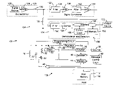
Referring to Figure 2, a wireless modem according to the present invention is
illustrated and is generally designated 100. The wireless modem 100 includes
an ERW
6
CA 02213619 1997-08-22
circuit 104 and a transponder 108. The memory 44 of the transponder 108 is
coupled
to the memory 112 of a host 116. As can be appreciated, the wireless modem 100
allows the memory 112 of the host 116 to be accessed remotely without
requiring
connection via direct electrical contact. In other words, data can be written
to or read
from the memory 112 of the host 116 in a contactless manner.
Various different ERWs 104 can be used depending upon the desired operating
range and frequency. A suitable ERW circuit 104 for short range applications
is the
MINIPROX Reader available from HID Corporation, Tustin, California, USA, that
can
be mechanically configured for mounting in various types of environments. The
ERW
circuit 104 has three main functional units: an exciter/writer (EW) circuit
120, a signal
conditioner circuit 122, and a demodulation and detection circuit 124.
The EW circuit 120 consists of an AC signal source 126 followed by a power
amplifier 128 that amplifies the signal generated by the AC signal source 126
to provide
a high current, high voltage excitation signal to a capacitor 130 and an
antenna coil
132. The inductance of the antenna coil 132 and the capacitance of the
capacitor 130
are selected to resonate at the excitation signal frequency so that the
voltage across
the antenna coil 132 is greater than the voltage output of the power amplifier
128. The
AC signal source 126 provides an RF excitation signal that can include a
password, an
identification code for the transponder 108, and/or a write signal to be
written into the
memory 44 of the transponder or the memory 112 of the host 116 to alter data
stored
therein.
The signal conditioner circuit 122 is also coupled to the antenna coil 132 and
serves to amplify the RF response signal generated by the transponder 108. The
signal conditioner circuit 122 filters out the RF excitation signal frequency
as well as
other noise and undesired signals outside of the frequency range of the
transponder
signals. The signal conditioner circuit 122 includes a first filter 134 that
passes the RF
response signal frequency returned from the transponder 108. A first amplifier
138
increases the signal strength of the signal output by the first filter 134. A
second filter
142 passively excludes high energy signals at the excitation frequency. A
second
amplifier 144 increases the signal strength of the signals output by the
second filter
142. Preferably the first and second filters 134 and 142 include bandpass and
7
CA 02213619 1997-08-22
bandstop filters. Skilled artisans can appreciate that the relative positions
of the first
and second filters can be switched or a higher order filter providing both
bandpass and
bandstop filtering functions can be employed. The first and second amplifiers
138 and
144 can be combined into a single amplifier.
The amplified output of the signal conditioner circuit 122 is input to a
filter 150
of the demodulation and detection circuit 124 that further reduces the RF
excitation
signal energy. Preferably the filter 124 is a low pass filter. The
demodulation and
detection circuit 124 also includes a demodulation circuit 154 and a
microcomputer that
is generally designated 156. The microcomputer 156 includes an input/output
interface
158, a memory 162, and a microprocessor or control logic 166. The demodulation
circuit 154 is typically a FSK demodulator that includes a phase-locked loop
circuit
configured as a tone detector. The demodulation circuit 154 and the
microcomputer
156 extract data from the RF response signal that includes data from the
memory 112
of the host 116. To extract the data, digital signals are generated when the
return
signal from the transponder 108 shifts between two frequencies. The timing of
the
transitions of the digital signals between the logic levels or frequencies is
detected. The
information obtained by the microcomputer 156 can be stored in the memory 162
or
transferred to an output device 170 such as a display, a printer, a network,
another
computer or other devices or storage media.
Figure 3a illustrates an exemplary application of the present invention. A
circuit
board 200 (analogous to the host 116 in Figure 2) is located within a computer
housing
202 of a computer 204. The circuit board 200 includes a microprocessor 206
coupled
to a non-volatile memory 208 (analogous to the host memory 112 in Figure 2). A
battery 214 coupled to the non-volatile memory 208 powers the non-volatile
memory
208 when the external power supply (not shown) of the computer 204 is
inoperative or
disconnected. The transponder 108 is preferably located adjacent the circuit
board 200
or is a plug-in module on the circuit board 200. The memory 44 of the
transponder 108
is connected by electrical contact to the non-volatile memory 208 of the
computer 204.
The ERW circuit 104 is maintained in a fixed position relative to the computer
204 by means of a fixture (not shown) or is alternatively portable. As can be
appreciated, the wireless modem of the present invention allows data to be
transmitted
8
CA 02213619 1997-08-22
to and/or read from the non-volatile memory 208 of the computer 204 to
facilitate
inventory control, reprogramming, repair, and diagnostics. In Figure 3b, the
transponder 108' is fabricated on the circuit board 200. The memory 44 of the
transponder 108' and the non-volatile memory 208 coupled to the microprocessor
206
are integrated into a non-volatile memory 218. The wireless modems in Figures
3a and
3b operate in a manner similar to the wireless modem 100 described above with
reference to Figure 2. The antenna coil 16 is preferably part of the artwork
of the
printed circuit board 200.
The non-volatile memory 208 or 218 of the computer 204 illustrated in Figures
3a and 3b commonly contains system information that is stored even when power
to
the computer 204 is off. The non-volatile memory 208 or 218 is typically
powered, even
when the computer 204 is switched off, by means such as a lithium battery.
Alternatively, the non-volatile memory may be of a type that retains
information, even
when there is a total absence of power, such as an EEPROM memory (not shown).
Using the wireless modem of the present invention, the contents of the memory
208 or
218 can be read and/or written to even if the computer 204 is off and/or not
functioning
properly due to software or hardware problems. The memory 208 or 218 can be
read
or written to in an electrical contact free manner and without requiring the
user interface
of the computer 204. An opening (not shown) may be required in the computer
housing
202, depending upon the construction of the computer housing 202 and upon the
frequency and signal strength of the RF excitation and response signals
generated by
the wireless modem, enabling the signals to pass into or out of the housing
202. If the
non-volatile memory is an EEPROM memory (not shown), the wireless modem
supplies
power thereto enabling the memory to be read.
In addition, the traditional use of the non-volatile memory can be extended to
include other information such as usage data (for example, time and date of
last use
and accumulated time of use), operational data (for example, the number of
disk
accesses and bad reads), service data (for example, the last date serviced and
items
replaced and/or repaired), and configuration data (for example, a manifest of
all
hardware and software items installed in the computer system). The
applications of
9
CA 02213619 1997-08-22
the wireless modem of the present invention include inventory control and
management, product billing, and problem diagnosis in the field.
For example, the system settings stored in the computer 204 may be incorrect
for the hardware or software installed on the computer 204. The incorrect
system
settings may prevent the computer 204 from booting up and/or operation of a
user
interface. A technician reads the data stored in the non-volatile memory using
the
wireless modem of the present invention to identify the installed hardware and
software
components from the manifest stored in the memory 208 or 218. The technician
compares the system settings stored in the non-volatile memory 208 or 218 with
the
correct system settings for the installed hardware and software components to
determine whether the settings are valid. If the system settings are
incorrect, the
technician writes correct system settings into the memory 208 or 218 using the
wireless
modem. If the system settings are correct, the technician accesses prior
service and
use information to further diagnose the malfunction.
Figure 4 illustrates one use for the wireless modems illustrated in Figures 3a
and
3b. As the computers 204 move down an assembly line 220 after assembly, the
ERW
circuit 104 transmits data to or reads data from the non-volatile memory 208
or 218
associated with the microprocessor 206. The ERW circuit 104 writes
configuration data
and system settings into the memory 208 and 218. Later, another ERW circuit
reads
the data for quality assurance, for generating a packing list with all
installed hardware
and software components, or other such applications. The ERW circuit 104
stores the
received data in the memory 162 (Figure 2) of the transponder 100 or outputs
the
received data to the output device 170. As can be appreciated, the ERW circuit
104
preferably reads the software and hardware manifest that details the installed
hardware
and software components on each computer for billing, inventory and pricing
purposes.
Figure 5 illustrates another suitable application for the wireless modem of
the
present invention. A portable ERW circuit 104' is used to read data from or
write data
to a non-volatile memory associated with one or more computers 204 located on
warehouse shelves 240. The retailer or wholesaler can use the information to
quickly
locate a computer having the desired software and hardware components
installed.
CA 02213619 1997-08-22
The wireless modem can also be used with other products that include a non-
volatile memory. For example, a non-volatile memory associated with
electronics of a
vehicle can be used to store use data (for example, time and date of last use
and
accumulated time of use), operational data (for example, number of miles
driven and
average speed), service data (for example, last date serviced and items
replaced
and/or repaired), vehicle data (for example, options installed on the vehicle
or
diagnostic data relating to failed parts). Skilled artisans can appreciate
that the wireless
modem can be used in numerous other applications such as with printers,
kitchen
appliances, cameras, heating and cooling controls and other electronic and
electro-
mechanical devices containing a non-volatile memory.
Referring to Figure 6, an alternate wireless modem is illustrated and is
generally
designated 300. The wireless modem 300 includes an ERW circuit 104 and a
transponder 304. The transponder 304 includes an analog front end 310 having
inputs
connected to a modulator 320, the antenna coil 16, the capacitor 18, and
outputs
connected to a write decoder 324 and a bitrate generator 328. An output of the
write
decoder 324 is connected to a first input of a mode register 336. The mode
register
336 has outputs coupled to the modulator 320 and a logic controller 338. A
second
input of the mode register 336 is coupled to a first output of the memory 340.
The first
and second outputs of the controller 338 are coupled to a first input of the
memory 340
and an input register 344 of the memory 340, respectively. A voltage generator
350
has an output coupled to the input register 344. The memory 340 is coupled to
the
memory 112 of a host 116. Skilled artisans can appreciate that the memory 340
of the
transponder 304 can be combined with the memory 112 of the host in a manner
similar
to the embodiment shown in Figure 3b.
The analog front end 310 generates power from the current induced on the
antenna coil 16 by an RF reading excitation signal or an RF write excitation
signal
(magnetic field) produced by the ERW circuit 104. The analog front end 310
controls
the bidirectional data communications with the ERW circuit 104. The analog
front end
310 rectifies the AC coil voltage to generate a DC supply voltage to power the
transponder 304 and extracts a clock signal from the AC coil voltage. The
analog front
end 310 selectively switches a load across opposite nodes of the antenna coil
16 for
11
CA 02213619 2000-10-16
data transmission from the transponder 304 to the ERW circuit 104. The analog
front
end 310 also detects a field gap that occurs when the ERW circuit 104 is
attempting to
write information into the memory 340 and/or the memory 112. As with the
embodiment illustrated in Figure 2, passwords for reading and writing can be
used.
The controller 338 loads the mode register 336 with operational data from the
memory 340 after power-on and periodically during reading to minimize errors.
The
controller 338 controls reading and writing access to the memory 340 and/or
the
memory 112. The controller 338 compares a password transmitted by the ERW
circuit
104 to the password stored in the memory 340 to grant or deny reading or
writing
access to the data stored in the memory 340.
The bitrate generator 328 allows the selection of bitrates that are a
fractional
portion of the frequency of the RF excitation signal. Typically, the bitrate
generator
allows selection of the following bitrate combinations: RF/8, RF/16, RF/32,
RF/40,
RF/50, RF/64, RF/100, and RF/128. Other bitrate combinations can be provided
if
desired. The write decoder 324 determines whether a write data stream from the
ERW
circuit 104 is valid. The voltage generator 350 generates a supply voltage for
programming the memory 340 or the memory 112 during a write data stream. The
mode register 336 stores the mode data from the memory 340 and periodically
refreshes the mode data during reading operation. The modulator 320 allows
selection
of various different modulation schemes including: frequency shift key (FSK);
phase
shift key (PSK); Manchester; biphase; and combinations thereof. The memory 340
is
preferably EEPROM.
The transponder 304 can be adapted from a Temic e5550 ReadIWrite
Identification Integrated Circuit (IDICc~) available from Temic Eurosil,
Eching, Germany,
by including the appropriate data input connections in a manner apparent to
the skilled
artisan applying the teaching of the present invention. Details of the Temic
e5550
IDIC~ are provided in "e5550 Standard RIW Identification IC Preliminary
Product
Features" dated October 13, 1994 and in "e5550 Standard R/W Identification IC
Preliminary Information" dated December 8, 1995.
12
CA 02213619 1997-08-22
While the foregoing preferred embodiments of the invention have been
described and shown, it is understood that alternatives and modifications,
such as
those suggested and others, may be made thereto and fall within the scope of
the
invention.
13