Note : Les descriptions sont présentées dans la langue officielle dans laquelle elles ont été soumises.
CA 022142~9 1997-08-27
-1 -
TM MODE DIELECTRIC RESONATOR AND TM MODE DIELECTRIC
FILTER AND DUPLEXER USING THE RESONATOR
BACKGROUND OF THE INVENTION
1. Field of the Invention
The present invention relates to a transverse magnetic
(TM) mode dielectric resonator and to a TM mode dielectric
and a TM mode dielectric duplexer using the resonator.
2. Description of the Related Art
As a dielectric filter using a TM mode dielectric
resonator, a dielectric filter having a structure such as
that shown in Fig. 13 is known. Each of dielectric
resonators shown in Fig. 13 is arranged as a dual mode type
in such a manner that dielectric blocks of short-circuit
type TM11o mode dielectric resonators are integrally combined
in a crisscross fashion. This structure enables one TM mode
dielectric resonator to have the function of two TM mode
dielectric resonators while being formed so as to be equal
in size to one ordinary dielectric resonator of this kind.
Referring to Fig. 13, a dielectric filter 101 has four
TM dual mode dielectric resonators 102, 103, 104, and 105,
which are arranged in a row with their openings facing in
the same direction. Metallic panels 106 and 107 are
attached to these dielectric resonators so as to cover the
openings.
CA 022142~9 1997-08-27
-2-
The TM dual mode dielectric resonator 102 has a cavity
casing 102a having openings on the front and rear sides as
viewed in Fig. 13, and a dielectric crisscross block 102XY.
The cavity casing 102a and the dielectric crisscross block
102XY are integrally formed of the same dielectric material.
A conductor 102b is formed on the outer surface of the
cavity casing 102a except on the front and rear opening
edges. The cavity casing 102a with the conductor 102b forms
a shielded cavity. The dielectric block 102XY is formed of
a horizontal portion 102X and a vertical portion 102Y as
viewed in Fig. 13. Thus, one TM dual mode dielectric
resonator 102 is formed as a two-stage resonator. Each of
the TM dual mode dielectric resonator 103, 104, and 105 has
the same structure as the TM dual mode dielectric resonator
102.
An input loop 108 and an output loop 109 are mounted on
che panel 106. The input loop 108 and the output loop 109
are connected to external circuits via coaxial connectors
(not shown).
Coupling loops 107a, 107b, 107c, and 107d for coupling
each adjacent pair of the TM dual mode dielectric resonators
are mounted on the panel 107.
In dielectric resonators for use in such a dielectric
filter, the resonant frequency of each dielectric resonator
is determined by the size of the cavity and the size of the
CA 022142~9 1997-08-27
-3-
dielectric block.
For example, in the case of an ordinary TM11o mode
dielectric resonator having a single vertical dielectric
block structure, the resonant frequency becomes lower if the
width of the cavity is increased while the width, thickness
and height of the dielectric block and the height of the
cavity are fixed. The resonant frequency becomes lower if
the width or thickness of the dielectric block is increased
while the size of the cavity is fixed. Also, when the
frequency is fixed, an increase in the unloaded Q of the
dielectric resonator is attained by increasing the height of
the dielectric block.
In such a case, if the height of the dielectric block
is increased, the height of the cavity is necessarily
increased. Since a real current flows through the conductor
on the cavity casing surface in the TM11o mode dielectric
resonator, the loss in the conductor on the cavity casing
surface becomes larger if the size of the cavity casing is
increased. However, an increase in unloaded Q achieved by
enlarging the cavity is sufficiently large in comparison
with the loss in the conductor on the cavity casing surface.
Consequently, the unloaded Q becomes higher if the height of
the dielectric block is increased.
If the loss in the conductor on the cavity casing
surface can be reduced, the unloaded Q can be increased
CA 022142~9 1997-08-27
-4-
while the increase in the height of the dielectric block is
limited. Therefore, there has been a need for a dielectric
resonator designed to reduce the loss in the conductor on
the cavity casing surface.
In the TM dual mode dielectric resonator shown in Fig.
13, when the sizes of the vertical and horizontal portions
of the dielectric block are adjusted according to a
predetermined frequency, the size of the cavity is also
determined. To increase the unloaded Q, therefore, it is
necessary to increase both the width and height of the
cavity, resulting in an increase in the overall size of the
dielectric filter. Also, the resonant frequency becomes
lower if the cavity size is increased while the size of the
dielectric block is fixed. Therefore, if the size of the
cavity is increased, the width or thickness of the
dielectric block is necessarily reduced. Thus, in the
conventional TM dual mode dielectric resonator, it is
difficult to independently change each of the unloaded Q and
the frequency.
SUk~RY OF THE INVENTION
In view of the above-described problems, an object of
the present invention is to provide a dielectric resonator
which has substantially no loss in the conductor on the
cavity casing surface, and in which the unloaded Q and the
CA 022142~9 1997-08-27
-5-
resonant frequency can be changed independently of each
other.
Another object of the present invention is to provide a
dielectric filter and a dielectric duplexer having an
improved unloaded Q and having a reduced thickness.
To achieve these objects, according to a first aspect
of the present invention, there is provided a TM mode
dielectric resonator comprising a shielded-cavity casing
having electrical conductivity, and at least one dielectric
block disposed in the shielded-cavity casing, wherein
electrodes are formed on two surfaces of the dielectric
block opposite from each other, and one of the two surfaces
on which the electrodes are formed is placed on an inner
surface of the shielded-cavity casing.
In this structure, substantially no real current flows
in the shielded-cavity casing corresponding to the cavity
casing of the conventional TM mode dielectric resonator.
According to a second aspect of the present invention,
a plurality of the above-described dielectric blocks are
superposed one on another so that at least one of the two
surfaces of each dielectric block on which the electrodes
are formed is in contact with the adjacent surface of
another of the dielectric blocks.
The unloaded Q of the resonator according to the first
aspect of the invention can be further improved by using
CA 022142~9 1997-08-27
-6--
this structure.
According to a third aspect of the present invention, a
plurality of the above-described dielectric blocks are
superposed one on another so that at least one of the two
surfaces of each dielectric block on which the electrodes
are formed is opposed to the adjacent surface of another of
the dielectric blocks while being spaced apart from the
same.
This structure enables use of the the dielectric
resonator of the present invention as a multi-stage
resonator.
According to a fourth aspect of the present invention,
a thin-film multilayer electrode formed by alternately
superposing a thin-film conductor and a thin-film dielectric
is used.
The loss in the electrodes formed on the upper and
lower surfaces of the dielectric block in the resonator
according to the first aspect of the invention can be
reduced if the electrodes are formed in this manner, thereby
further improving the unloaded Q.
According to a fifth aspect of the present invention,
the dielectric block is formed into a cylindrical shape.
The loss at the edge of the electrode can be reduced
thereby relative to that in the electrode on a dielectric
block in the form of a polygonal prism.
CA 022142~9 1997-08-27
According to a sixth aspect of the present invention,
the above-described TM mode dielectric resonator is
externally coupled to input and output means.
A dielectric filter having a high unloaded Q can be
obtained by being constructed in this manner.
According to a seventh aspect of the present invention,
coupling means are disposed between the TM mode dielectric
resonator and the input and output means.
It is possible to easily control the degree of coupling
between the TM mode dielectric resonator and the input and
output means by changing, adding or removing coupling means.
According to an eighth aspect of the present invention,
coupling means are disposed between a plurality of TM mode
dielectric resonators.
It is possible to easily control the degree of coupling
between the TM mode dielectric resonators by changing,
adding or removing coupling means.
According to a ninth aspect of the present invention,
the coupling means comprises an electrode sheet formed of a
dielectric sheet and an electrode formed on one surface of
the dielectric sheet.
It is possible to easily obtain the desired degree of
coupling by suitably selecting the dielectric constant of
the dielectric and the size of the electrode sheet.
According to a tenth aspect of the present invention,
CA 022142~9 1997-08-27
-8-
in a plurality of TM mode dielectric resonators, the
resonant frequency of the initial-stage and final-stage in
the state of operating alone is increased relative to the
resonant frequency of the other TM mode dielectric
resonators, thereby equalizing the resonant frequencies of
the TM mode dielectric resonators when the resonators form a
dielectric filter.
According to an eleventh aspect of the present
invention, a plurality of TM mode dielectric filters
described above are combined to form a first TM mode
dielectric filter having a first frequency band and a second
TM mode dielectric filter having a second frequency band,
and the first frequency band and the second frequency band
are made different from each other.
In this manner, a dielectric duplexer having a higher
unloaded Q can be obtained.
According to a twelfth aspect of the present invention,
the shape of the TM mode dielectric resonator forming the
first TM mode dielectric filter and the shape of the TM mode
dielectric resonator forming the second TM mode dielectric
filter are made different from each other to make the first
frequency band and the second frequency band different from
each other.
A need for adding a circuit for relatively shifting the
frequency bands is thereby eliminated while such a circuit
CA 022142~9 1997-08-27
_9 _
is required in the case of using TM mode dielectric
resonators equal in shape.
According to a thirteenth aspect of the present
invention, the first TM mode dielectric filter is used as a
transmitting filter while the second TM mode dielectric
filter is used as a receiving filter.
In this manner, a TM mode dielectric duplexer used for
a transmitter-receiver and having a higher unloaded Q can be
obtained.
BRIEF DESCRIPTION OF THE DRAWINGS
Fig. lA is a partially fragmentary perspective view of
a dielectric filter which represents a first embodiment of
the present invention;
Fig. lB is a cross-sectional view taken along the line
A-A of Fig. lA;
- Fig. 2A is a partially fragmentary perspective view of
a dielectric filter which represents a second embodiment of
the present invention;
Fig. 2B is a cross-sectional view taken along the line
B-B of Fig. 2A;
Fig. 3A is a partially fragmentary perspective view of
a modification of the dielectric filter shown in Figs. 2A
and 2B;
Fig. 3s is a cross-sectional view taken along the line
CA 022142~9 1997-08-27
-1 O-
C-C of Fig. 3A;
Fig. 4A is a partially fragmentary perspective view of
a dielectric filter which represents a third embodiment of
the present invention;
Fig. 4B is a cross-sectional view taken along the line
D-D of Fig. 4A;
Fig. 5A is a partially fragmentary perspective view of
a dielectric filter which represents a fourth embodiment of
the present invention;
Fig. 5B is a cross-sectional view taken along the line
E-E of Fig. SA;
Fig. 6 comprises plan views of inner portions of upper
and lower sections of the dielectric filter shown in Figs.
SA and 5B;
Fig. 7 is a cross-sectional view of a modification of
the dielectric filter shown in Figs. 5A, 5B, and 6;
Fig. 8 is a partially fragmentary perspective view of a
dielectric duplexer which represents a fifth embodiment of
the present invention;
Fig. 9 is an exploded perspective view of the
dielectric duplexer shown in Fig. 8;
Fig. 10 is a cross-sectional view of a modification of
the dielectric duplexer shown in Fig. 8 and 9;
Fig. 11 is a cross-sectional view of another
modification of the dielectric duplexer shown in Fig. 8 and
CA 022142~9 1997-08-27
-1 1-
9;
Fig. 12 is a cross-sectional view of a dielectric
filter which represents a sixth embodiment of the present
invention; and
Fig. 13 is an exploded perspective view of a
conventional TM mode dielectric filter.
DESCRIPTION OF THE PREFERRED EMBODIMENTS
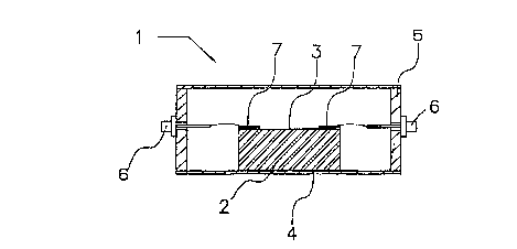
A dielectric filter which represents a first embodiment
of the present invention will be described with reference to
Figs. lA and lB. Fig. lA is a partially fragmentary
perspective view of a dielectric filter 1, and Fig. lB is a
cross-sectional view taken along the line A-A of Fig. lA.
As shown in Figs. lA and lB, the dielectric filter 1
has a dielectric block 2 provided in a casing 5 made of a
metal and forming a shielded cavity.
The dielectric block 2 is a cylindrical member formed
of a dielectric material. Electrodes 3 and 4 are formed on
two opposite surfaces of the dielectric block 2. The
dielectric block 2 is placed so that the electrode 4 is in
contact with an inner bottom surface of the shielded-cavity
casing 5. The electrode 4 is fixed and electrically
connected to the shielded-cavity casing 5 by soldering or
the like. The electrode 3 of the dielectric block 2 faces
an inner ceiling surface of the shielded-cavity casing 5 and
CA 022l42~9 l997-08-27
-12-
is uniformly spaced apart from this surface. When a high-
frequency signal is input to the thus-constructed dielectric
filter 1, an electric field is generated between the
electrodes 3 and 4 in the dielectric block 2 and a magnetic
field is generated along the circumference of the dielectric
block 2. As a result, an electromagnetic field is
concentrated at and confined in the dielectric block 2 in an
electromagnetic field distribution approximate to a TMo1o
mode. At this time, the dielectric block 2 functions as a
one-stage dielectric resonator.
A pair of coaxial connectors 6 for external input and
output are attached to side wall potions of the shielded-
cavity casing 5. Center electrodes of the coaxial
connectors 6 are electrically connected to electrodes sheets
7 by, for example, wires.
Each of the electrode sheets 7 is formed of a sheet of
an insulating material such as a resin and an electrode film
formed on the upper surface of the insulating material
sheet. No electrode film is formed on the lower surface of
the insulating material sheet. The electrode sheets 7 are
disposed on and attached to the electrode 3 formed on the
upper surface of the dielectric block 2. The lower surfaces
of the electrode sheets 7, on which no electrode film are
formed, are brought into contact with the electrode 3.
The thus-constructed dielectric filter 1 functions as
CA 022l42~9 l997-08-27
-13-
described below.
A high-frequency signal is input to one of the coaxial
connectors 6. The capacitance across the insulating
material between the electrode 3 of the dielectric block 2
and the electrode film on the upper surface of one of the
electrode sheets 7 connected to the center electrode of the
coaxial connector 6 acts for coupling between the center
electrode of the coaxial connector 6 and the dielectric
block 2. The dielectric block 2 resonates with the input
signal by this coupling. A signal is thereby output through
the capacitance of the other electrode sheet 7 and through
the other coaxial connector 6 connected to the electrode
film on this electrode sheet 7.
The thus-arranged dielectric filter can be much smaller
in thickness than the conventional dielectric filter using
short-circuit type TM11o mode dielectric resonators. The
resonant frequency and the unloaded Q of the dielectric
filter of this embodiment are determined by the same factors
as the conventional dielectric filter using short-circuit
type TM11o mode dielectric resonators. That is, the resonant
frequency is determined by the sectional area along a plane
perpendicular to the direction of height while the unloaded
Q is determined by the height of the dielectric block. In
this embodiment, however, substantially no real current
flows through the side surface of the shielded-cavity casing
CA 022142~9 1997-08-27
-14-
corresponding to the conventional cavity casing.
Accordingly, substantially no deterioration in unloaded Q
results with respect to this portion. Consequently, the
increase in the height of the dielectric block necessary for
obtaining the desired unloaded Q can be limited, thereby
limiting the increase in the height of the entire dielectric
filter.
The embodiment of the present invention has been
described with respect to use of a cylindrical dielectric
block. However, such a cylindrical dielectric block is not
exclusively used and dielectric blocks having any other
shapes may also be used as long as they have electrodes
corresponding to the two electrodes 3 and 4 shown in Fig. 1.
Among such dielectric blocks usable in accordance with
the present invention, however, a cylindrical dielectric
block, such as the dielectric block 2 of the embodiment
described above, is used particularly advantageously for a
reason described below. In the surface of such a
cylindrical dielectric block on which an electrode is
formed, the distance from the center of the circle to the
edge of the circuit, i.e., the circumferential, is constant.
In other dielectric blocks in the form of polygonal prisms,
the distance from the center to the vertices of the
polygonal shape is different from the distance from the
center to other edge portions. In such dielectric blocks,
CA 022l42~9 l997-08-27
-15-
therefore, a potential difference occurs to cause a current
at the edge of the electrode along the polygonal shape,
resulting in occurrence of a loss in the electrode. In
contrast, in a cylindrical dielectric block, substantially
no current flows due to such a potential difference since
the distance between the center of the circle and the
circumferential end of the surface on which the electrode is
formed is constant. The resulting loss in this case is
advantageously small. Because of the above-described effect
of using a cylindrical shape, a superconductor, with which a
serious problem of loss at the electrode edge may arise, can
be used as electrodes 3 and 4. If a superconductor is used
as electrodes 3 and 4, a dielectric resonator or filter
having a higher unloaded Q can be obtained.
A second embodiment of the present invention will next
be described with reference to Figs. 2A and 2B. Fig. 2A is
a partially fragmentary perspective view and Fig. 2B is a
cross-sectional view taken along the line B-B of Fig. 2A.
Components of this embodiment identical to those of the
first embodiment are indicated by the same reference
numerals and will not be described in detail.
Referring to Figs. 2A and 2B, a dielectric filter 11
has dielectric blocks 12a and 12b disposed in a metallic
shielded-cavity casing 5.
Electrodes 13a and 14a are formed on two opposite
CA 022142~9 1997-08-27
-16-
surfaces of the dielectric block 12a. Electrodes 13b and
14b are formed on two opposite surfaces of the dielectric
block 12b. The electrode 13a of the dielectric block 12a is
fixedly connected to an inner ceiling surface of the
shielded-cavity casing 5 by soldering or the like while the
electrode 14b of the dielectric block 12b is fixedly
connected to an inner bottom surface of the shielded-cavity
casing 5 by soldering or the like. The electrode 14a of the
dielectric block 12a and the electrode 13b of the dielectric
block 13b are electrically connected to each other.
Electrode sheets 7 are formed in the same manner as
those in the first embodiment. Each of electrode sheets 7
is attached to the joint between the dielectric blocks 12a
and 12b, the surface of the electrode sheet 7 on which no
electrode film is formed being in contact with the
dielectric blocks 12a and 12b. If the balance of an
electromagnetic field distribution through the upper and
lower dielectric blocks is considered, it is preferable to
attach the electrode sheets 7 to the joint between the
dielectric blocks 12a and 12b. However, the electrode
sheets 7 may be attached to other portions.
The center electrodes of the coaxial connectors 6
attached to side surfaces of the shielded-cavity casing 5
are electrically connected to the electrode films on the
electrode sheets 7 by, for example, wires. The center
CA 022l42~9 l997-08-27
-17-
electrodes of the coaxial connectors 6 may be directly
connected to the electrodes 13b and 14a without using
electrode sheets 7. In such a case, a wide-band dielectric
filter can be formed because the degree of external coupling
is maximized.
The thus-constructed dielectric filter 11 functions as
a one-stage dielectric filter and has an improved unloaded Q
in comparison with the dielectric filter of the first
embodiment if these dielectric filters are equal in height.
A modification of this embodiment such as that shown in
Figs. 3A and 3B may be made. Fig. 3A is a partially
fragmentary perspective view and Fig. 3B is a cross-
sectional view taken along the line C-C of Fig. 3A.
Components of this embodiment identical to those of the
first or second embodiment are indicated by the same
reference numerals and will not be described in detail.
Referring to Fig. 3A and 3B, dielectric blocks 22a and
22b constructed in the same manner as the dielectric block 2
shown in Figs. lA and lB and the dielectric blocks 12a and
12b shown in Figs. 2A and 2B are placed in a shielded-cavity
casing 5. A dielectric block 22c, newly provided, is
interposed between the dielectric blocks 22a and 22b, thus
constructing a dielectric filter 21. In this arrangement,
the dielectric blocks 22a and 22c form one-stage resonator
and the dielectric blocks 22b and 22c also form one-stage
CA 022142~9 1997-08-27
-18-
resonator. Accordingly, the dielectric blocks 22a to 22c
superposed one on another in the dielectric filter 21 shown
in Figs. 3A and 3B function as a dual mode dielectric
resonator, so that the dielectric filter 21 can be used as a
filter having a two-stage resonator. On the basis of this
structure, a dielectric filter having n-l dielectric
resonator stages may be constructed by further superposing
dielectric blocks so as to form a stack of n dielectric
blocks.
The above-described TM dual mode dielectric resonator
of this embodiment having the structure shown in Figs. 3A
and 3B uses dielectric blocks thin enough to reduce the
overall thickness relative to that of the conventional
short-circuit type TM dual mode dielectric resonator having
the same resonant frequency.
In this embodiment, as well as in the first embodiment,
the shape of the dielectric blocks is not limited to a
cylindrical shape and may have the shape of any polygonal
prism. However, it is preferred that each of the dielectric
blocks be formed into a cylindrical shape for the reason
described above with respect to the first embodiment. Also,
the shapes of the plurality of dielectric blocks of the
dielectric filter shown in Figs. 2A and 2B or 3A and 3B may
be varied.
A third embodiment of the present invention will next
CA 022142~9 1997-08-27
-1 9 -
be described with reference to Figs. 4A and 4B. Fig. 4A is
a partially fragmentary perspective view and Fig. 4B is a
cross-sectional view taken along the line D-D of Fig. 4A.
Components of this embodiment identical to those of the
first or second embodiment are indicated by the same
reference numerals and will not be described in detail.
Referring to Fig. 4A and 4B, a dielectric filter 31 has
such a structure that an electrode 34a of a dielectric block
32a and an electrode 33b of a dielectric block 32b are
electrically insulated from each other by spacing
therebetween. The dielectric blocks 32a and 32b function as
resonators independent of each other, such that the
dielectric filter 31 is formed of a two-stage resonator.
A coupling control plate 39 having a coupling control
hole 39a formed generally at its center is disposed between
the electrode 34a of the dielectric block 32a and the
electrode 33b of the dielectric block 32b. The degree of
coupling between the resonator formed by the dielectric
block 32a and the resonator formed by the dielectric block
32b is controlled by selecting the size of the coupling
control hole 39a. If the coupling control hole 39a is
larger, the degree of coupling between the resonator formed
by the dielectric block 32a and the resonator formed by the
dielectric block 32b is higher. If the coupling control
hole 39a is smaller, the degree of coupling between the
CA 022142~9 1997-08-27
-20-
resonator formed by the dielectric block 32a and the
resonator formed by the dielectric block 32b is lower.
In this embodiment, as well as in the first and second
embodiments, the shape of the dielectric blocks is not
limited to a cylindrical shape. However, it is preferred
that each of the dielectric blocks be formed into a
cylindrical shape for the reason described above with
respect to the first embodiment. Also, the shapes of the
two dielectric blocks used may be different from each other.
A fourth embodiment of the present invention will next
be described with reference to Figs. 5A, 5B, and 6. Fig. 5A
is a partially fragmentary perspective view and Fig. 5B is a
cross-sectional view taken along the line E-E of Fig. 5A.
Fig. 6 comprises plan views of upper and lower sections of
the dielectric filter shown in Figs. SA and 5B. Supporting
members 48 shown in Figs. 5B are omitted in Fig. 6. In this
embodiment, a dielectric filter 41 formed of a four-stage
resonator is constructed by disposing, in a side-by-side
fashion, two dielectric filters 31 described above as the
third embodiment. Components of this embodiment identical
to those of the first, second or third embodiment are
indicated by the same reference numerals and will not be
described in detail.
Referring to Fig. 5A and 5B, the dielectric filter 41
has four cylindrical dielectric blocks 42a to 42d, and pairs
CA 022142~9 1997-08-27
-21-
of electrodes 43a and 44a, 43b and 44b, 43c and 44c, and 43d
and 44d are respectively formed on two major opposite
surfaces of the dielectric blocks 42a to 42d.
The structure of each of the dielectric blocks 42a to
42d is the same as that of the above-described dielectric
blocks of the first to third embodiments, and will not be
described in detail.
The shielded-cavity casing 45 is formed of a dielectric
material having the same thermal expansion coefficient as
the dielectric blocks 42a to 42d, and an electrode 45a
formed on its outer surface and, therefore, has the same
shielding function as a metallic shielded-cavity casing.
Since the shielded-cavity casing 45 has the same thermal
expansion coefficient as the dielectric blocks, it is free
from the problem of the difference between the thermal
expansion coefficients of a metal and a dielectric. The
shielded-cavity casing 45 is formed by combining separate
upper and lower sections. Recesses for accommodating the
dielectric blocks 42a to 42d are formed in each of the upper
and lower sections. Further, input/output electrodes 46 are
formed on one of the side surfaces of the shielded-cavity
casing 45 while being electrically separated from the
electrode 45a formed on the outer surface of the shielded-
cavity casing 45. The input/output electrodes 46 extend
vertically from the bottom surface of the shielded-cavity
CA 022142~9 1997-08-27
-22-
casing 45 used as a mounting surface.
One of the input/output electrodes 46 is coupled to the
dielectric block 42b through an electrode sheet 7. The
dielectric block 42b is coupled to the dielectric block 42a
uniformly spaced apart from the dielectric block 42b. The
dielectric block 42a is in turn coupled to the dielectric
block 42c adjacent to the dielectric block 42a through an
electrode sheet 7. Further, the dielectric block 42c is
coupled to the dielectric block 42d uniformly spaced apart
from the dielectric block 42c. The dielectric block 42d is
coupled to the other input/output electrode 46 through an
electrode sheet 7.
Supporting member 48 made of a dielectric material
having a smaller dielectric constant is disposed between the
dielectric blocks 42a and 42b uniformly space these
dielectric blocks from each other. Another supporting
member 48 is disposed between the dielectric blocks 42c and
42d for the same purpose. A coupling control plate 49 made
of a metal is integrally combined with each supporting
member 48 by being partially embedded in the supporting
member 48. Each coupling control plate 49 has a coupling
control holed 49a for controlling the coupling between the
dielectric blocks 42a and 42b or the dielectric blocks 42c
and 42d
The thus-constructed dielectric filter can be obtained
CA 022142~9 1997-08-27
-23-
as a filter smaller in thickness and capable of being
mounted in a surface mount manner.
The dielectric blocks 42a to 42d may have different
characteristic resonant frequencies. That is, in the
dielectric blocks 42b and 42d coupled to the input/output
electrodes 46 and respectively forming the initial-stage
and final-stage dielectric resonators, the circumferential
side surface on which no electrode is formed is partially
cut off to adjust the resonance frequency of the
corresponding dielectric resonator to a frequency higher
than that of the resonators formed by the other dielectric
blocks 42a and 42c. This is because, when input and output
means are respectively coupled to the initial-stage and
final-stage dielectric resonators by capacitive coupling,
the capacitance due to each coupling reduces the apparent
resonant frequency of each of the initial-stage and final-
stage dielectric resonators by such an amount that the
desired filtering characteristic of the dielectric filter
formed by the dielectric resonators cannot be obtained.
That is, to present this phenomenon, the resonant frequency
of each of the initial-stage and final-stage dielectric
resonators in the state of operating alone is increased so
that the apparent resonant frequencies of all the dielectric
resonators become approximately equal to each other when the
dielectric resonator is formed.
CA 022142~9 1997-08-27
-24-
A structure such as shown in Fig. 7 may alternatively
be used as means for increasing the resonant frequency of
each of the initial-stage and final-stage dielectric
resonators. Fig. 7 is a cross-sectional view of a
dielectric filter 41a corresponding to the cross section of
the dielectric filter shown in Fig. 5B.
As shown in Fig. 7, dielectric blocks 42e and 42f
smaller in diameter than the dielectric blocks 42b and 42d
forming the initial-stage and final-stage dielectric
resonators are provided in place of the dielectric blocks
42b and 42d. That is, the dielectric block 42e is provided
in the initial stage while the dielectric block 42f having
the same diameter as the dielectric block 42e is provided in
the final stage, thereby increasing the resonant frequency
of each of the initial-stage and final-stage dielectric
resonators in the state of operating alone.
In this embodiment, as well as in the first to third
embodiments, the shape of the dielectric blocks is not
limited to a cylindrical shape. However, it is preferred
that each of the dielectric blocks be formed into a
cylindrical shape for the reason described above with
respect to the first embodiment. Also, the shape of one of
the plurality of dielectric blocks may be changed. In this
embodiment, the input and output means are not coaxial
connectors such as those used in the first, second or third
CA 022142~9 1997-08-27
-25-
embodiment but surface mount type input/output electrodes.
In this embodiment, however, coaxial connectors arranged in
the same manner as those in the first, second or third
embodiment may alternatively be used. Needless to say, the
input/output electrode structure of this embodiment suitable
for surface mounting may be used in place of the coaxial
connectors in the dielectric filters described above as the
first to third embodiments.
A fifth embodiment of the present invention will next
be described with reference to Figs. 8 and 9. Fig. 8 is a
partially fragmentary perspective view and Fig. 9 is an
exploded perspective view. Components of this embodiment
identical to those of the first, second, third or fourth
embodiment are indicated by the same reference numerals and
will not be described in detail.
Referring to Fig. 8, a dielectric duplexer 51 is formed
of a first dielectric filter 51a having a first frequency
band and a second dielectric filter 51b having a second
frequency band.
The first dielectric filter 51a is formed of dielectric
blocks 52a to 52d shown in Fig. 9. In the dielectric filter
51a, a coaxial connector 56a is coupled to the dielectric
block 52b through an electrode sheet 7, and the dielectric
block 52b is coupled to the dielectric block 52a. The
dielectric block 52a is coupled to the dielectric block 52c
CA 022142~9 1997-08-27
-26-
through an electrode sheet 7. The dielectric block 52c is
coupled to the dielectric block 52d, which is coupled to a
coaxial connector 56b through an electrode sheet 7 and a
coil L1 and a capacitor C1 provided as matching means.
Thus, the dielectric filter 51a having a four-stage
dielectric resonator is formed, as shown in Fig. 8.
The second dielectric filter 51b is formed of
dielectric blocks 52e to 52h shown in Fig. 9. In the
dielectric filter 51b, a coaxial connector 56b is coupled to
the dielectric block 52f through a capacitor C1 and a coil
L1 provided as matching means and through an electrode sheet
7. The dielectric block 52f is coupled to the dielectric
block 52e. The dielectric block 52e is coupled to the
dielectric block 52g through an electrode sheet 7. The
dielectric block 52g is coupled to the dielectric block 52h,
which is coupled to a coaxial connector -56c through an
electrode sheet 7. Thus, the dielectric filter 51b having a
four-stage dielectric resonator is formed, as shown in Fig.
8.
As shown in Fig. 9, a shielded-cavity casing 55 is
formed by combining separate upper and lower sections.
Recesses for accommodating the dielectric blocks 52a to 52h
are formed in each of the upper and lower sections.
The dielectric blocks 52a to 52h are electrically
connected to recessed surfaces of the shielded-cavity casing
CA 02214259 1997-08-27
-27-
55 by annular grounding plates 60.
As shown in Fig. 9, sets of supporting members 58 for
supporting the dielectric blocks 52a to 52h and a coupling
control plate 59 supported by being interposed between upper
and lower supporting members 58 are provided between the
groups of dielectric blocks 52a, 52c, 52e, and 52g and the
group of dielectric blocks 52b, 52d, 52f, and 52h.
Supporting members 58 are made of a material having a
small dielectric constant. Three supporting members 58 form
one set for supporting one dielectric block in a three-point
supporting manner. Cuts 58a are formed in the supporting
members 58 to enable the electrode sheets 7 to be fixed by
being pinched between the dielectric blocks and the
supporting members 58a.
Coupling control holes 59a are formed in the coupling
control plate 59. The diameter and the shape of the
coupling control holes 59a are selected to control coupling
between the dielectric blocks 52a and 52b, between the
dielectric blocks 52c and 52d, between the dielectric blocks
52e and 52f and between the dielectric blocks 52g and 52h.
The thus-constructed dielectric duplexer 51 can be
obtained as a small-loss thin duplexer formed of an eight-
stage dielectric resonator.
The initial-stage and final-stage dielectric blocks of
the dielectric filters 51a and 52b of the dielectric
CA 022142~9 1997-08-27
-28-
duplexer 51 may be reduced in diameter, as are those in the
above-described modification of the fourth embodiment.
Fig. 10 is a cross-sectional view of a dielectric
duplexer 61 in which the diameters of the initial-stage and
final-stage dielectric blocks of each of dielectric filters
are reduced. A structure about coaxial connectors of this
dielectric duplexer is the same as that in the dielectric
duplexer 51 shown in Figs. 8 and 9, and the description for
it will not be repeated.
As shown in Fig. 10, the diameters of the dielectric
blocks 62b, 62d, 62f, and 62h corresponding to the initial
and final stages of the dielectric filters are reduced
relative to those of the other dielectric blocks 62a, 62c,
62e, and 62g.
The shapes of supporting members 68a and grounding
plates 60a for supporting the dielectric blocks 62b, 62d,
o2f, and 62h are also changed according to the sizes of
these dielectric blocks.
In this manner, the resonant frequencies of the
initial-stage and final-stage dielectric resonators in the
state of operating alone are increased to ensure that, in
each of the first and second dielectric filters, the
apparent resonant frequencies of the dielectric resonators
are approximately equal to each other. Needless to say, the
apparent resonant frequency of the dielectric resonators
CA 022142~9 1997-08-27
-29-
forming the first dielectric filter and the apparent
resonant frequency of the dielectric resonators forming the
second dielectric filter are set so as to be different from
each other.
A structure such as that as shown in Fig. 11 can also
be used as a structure for enabling the first and second
dielectric filters to have different frequency bands. A
structure about coaxial connectors of the dielectric
duplexer shown in Fig. 11 is the same as that in the
dielectric duplexer 51 shown in Figs. 8 and 9, and the
description for it will not be repeated.
As shown in Fig. 11, dielectric blocks 72a to 72d
forming a first dielectric filter and dielectric blocks 72e
to 72h forming second dielectric filter are made different
in shape from each other; the dielectric blocks 72a to 72d
are smaller in diameter than the dielectric blocks 72e to
72h, thereby enabling the first and second dielectric
filters to have different frequency bands. While in this
modification the diameters of dielectric blocks are made
different from each other, any other various means for
setting different frequency bands, e.g., making rectangular
and cylindrical dielectric blocks, are also possible. The
frequency bands of the first and second dielectric filters
may be made different from each other by adding reactance
elements such as capacitors and inductors without changing
CA 022142~9 1997-08-27
-30-
the shape of the dielectric blocks or by cutting the
dielectric blocks.
Each of the dielectric duplexers shown in Figs. 8 to 11
can be used as a common antenna device for a transmitter-
receiver in such a manner that the first frequency band of
the first dielectric filter is used as a receiving frequency
band of a receiving filter while the second frequency band
is used as a transmitting frequency band of a transmitting
filter. Also, the first and second dielectric filters may
be used as two transmitting filters or two receiving
filters.
A sixth embodiment of the present invention will next
be described with reference to Fig. 12. This embodiment
uses the same construction as that of the dielectric filter
1 shown in Fig. 1. Components or portions identical or
corresponding to those shown in Fig. 1 are indicated by the
same reference numerals and will not be described in detail.
A dielectric filter 81 shown in Fig. 12 differs from
the dielectric filter 1 shown in Fig. 1 in the structure of
electrodes formed on the dielectric block. That is, while
each of the electrodes 3 and 4 of the dielectric block 2 in
the dielectric filter 1 shown in Fig. 1 is formed of a
single-layer conductor, each of electrodes 83 and 84 of a
dielectric block 82 in the dielectric filter 81 shown in
Fig. 12 is formed of a thin-film multilayer electrode formed
CA 022l42~9 l997-08-27
-31-
by alternately laminating a thin-film conductor and a thin-
film dielectric. Such a thin-film multilayer electrode,
e.g., one described in Japanese Patent Application No.
310900/1994, can be used with a reduced insertion loss in
comparison with a single-layer conductor. Therefore, if
such an thin-film multilayer electrode is used in a
resonator, the resonator can have a higher unloaded Q.
An arrangement using a thin-film multilayer electrode
in the dielectric filter shown in Fig. 1 has been described
as the sixth embodiment by way of example. Needless to say,
such a thin-film multilayer electrode can also be applied to
each of the dielectric filters of the second to fourth
embodiments and the dielectric duplexer of the fifth
embodiment to obtain a dielectric filter or dielectric
duplexer having a higher unloaded Q.
According to the present invention, substantially no
real current flows in the shielded-cavity casing for
accommodating the dielectric block, so that there is
substantially no loss in the shielded cavity casing. As a
result, a dielectric resonator, a dielectric filter and a
dielectric duplexer each having a high unloaded Q can be
obtained.
According to the second aspe~t of the present
invention, a plurality of dielectric blocks are disposed in
a space where an electromagnetic field distribution is
CA 022142~9 1997-08-27
-32-
generated, thereby making it possible to obtain a dielectric
resonator, a dielectric filter and a dielectric duplexer
each having a higher unloaded Q.
According to the third aspect of the present invention,
a plurality of dielectric blocks are arranged in the
direction of height while being spaced apart from each other
to form a multi-stage resonator, thereby achieving a
reduction in bottom surface area.
According to the fourth aspect of the present
invention, a thin-film multilayer electrode is used to
obtain a dielectric resonator, a dielectric filter and a
dielectric duplexer each having a much higher unloaded Q.
According to the fifth aspect of the present invention,
the dielectric block is formed into a cylindrical shape such
that the edge of the electrode surface is at a constant
distance from the center of the surface, thereby preventing
occurrence of a potential difference and, hence, a current
at the edge. The loss in the electrode can be further
reduced thereby. As a result, a dielectric resonator having
a higher unloaded Q can be obtained.
According to the ninth aspect of the present invention,
an electrode sheet formed of a dielectric sheet and an
electrode formed on one surface of the dielectric sheet is
used as a coupling means, and the desired degree of coupling
can easily be achieved by suitably selecting the dielectric
CA 022142~9 1997-08-27
-33-
constant of the dielectric and the size of the electrode
sheet.
According to the tenth aspect of the present invention,
the resonant frequency of the initial-stage and final-stage
TM mode dielectric resonators in the state of operating
alone is increased, thereby equalizing the resonant
frequencies of the TM mode dielectric resonators when the
resonators form a dielectric filter.
According to the eleventh aspect of the present
invention, a plurality of TM mode dielectric filters
described above are combined to form a first TM mode
dielectric filter having a first frequency band, and a
second TM mode dielectric filter having a second frequency
band, and the first frequency band and the second frequency
band are made different from each other, thereby obtaining a
dlelectric duplexer having a higher unloaded Q.
- According to the twelfth aspect of the present
invention, the shape of TM mode dielectric resonator forming
the first TM mode dielectric filter and the shape of the TM
mode dielectric resonator forming the second TM mode
dielectric filter are made different from each other to make
the first frequency band and the second frequency band
different from each other. A need for adding a circuit for
relatively shifting the frequency bands is thereby
eliminated while such a circuit is required in the case of
CA 02214259 1997-08-27
-34-
using TM mode dielectric resonators equal in shape.