Note : Les descriptions sont présentées dans la langue officielle dans laquelle elles ont été soumises.
CA 02214624 1997-09-0~
~,
. .
DIGITAL AMPLITUDE MODULATION AMPLIFIER
AND TELEVISION BROADCASTING MACHINE
BACKGROUND OF THE INVENTION
1. Field of the Invention:
This invention relates to a digital amplitude
modulation amplifier, and more particularly to a
digital amplitude modulation amplifier which converts a
modulation signal into a digital signal, power
amplifies a transmission carrier in accordance with the
digital signal and outputs an amplitude modulated wave.
The present invention relates also to a television
broadcasting machine, and more particularly to a
television broadcasting machine which can transmit a
vestigial side band modulated (VSB) television
broadcasting signal by phase modulating and amplitude
modulating a carrier with phase information and
amplitude information obtained from a video signal.
2. Description of the Related Art:
Fig. 1 shows a block diagram of an example of a
conventional amplitude modulation amplifier. Referring
to Fig. l, a carrier outputted from carrier generator
ll and a modulation signal outputted from modulation
signal generator 12 are supplied to amplitude modulator
41, by which an amplitude modulated wave is produced by
modulating the amplitude of the carrier with the
CA 02214624 1997-09-0~
modulation signal. The amplitude modulated wave is
supplied to and power amplified by linear power
amplifier 42 which performs an A class or AB class
operation. Consequently, the carrier (amplitude
modulated wave) whose amplitude is modulated in
accordance with the modulation signal is outputted from
linear power amplifier 42.
Fig. 2 shows a block diagram of an example of a
conventional digital amplitude modulation amplifier.
This conventional digital amplitude modulation
amplifier is disclosed in U.S. Patent No. 4,804,931 and
can control the output level thereof with a digital
signal in the form of a modulation signal.
Referring to Fig. 2, an analog modulation signal
generated from modulation signal generator 12 is
supplied to A/D converter 13, by which it is converted
into a digital modulation signal. The digital
modulation signal is supplied to on/off controller 14,
by which it is converted into a control signal for
on/off switching four switches SWl to SW4. Here, since
four switches SW1 to SW4 are involved, the quantization
bit number of the output digital signal of A/D
converter 13 described above is 4 bits, and the control
signal mentioned above on/off switches switches SW1 to
SW4 corresponding to the individual bits.
Switches SW1 to SW4 receive a carrier generated by
CA 02214624 1997-09-0~
carrier generator 11 as input signals thereto and
supply the inputted carriers to power amplifiers PA1 to
PA4 provided corresponding thereto for periods for
which they are controlled to an on state. Since a
linear characteristic is not required for power
amplifiers PAl to PA4, they are constructed so as to
effect a C class operation in which they exhibit a high
power utilization efficiency. Further, power
amplifiers PAl to PA4 have amplification degrees
weighted for the individual bits of the digital signal
of 4 bits. For example, power amplifier PAl has an
amplification degree which increases in proportion to
23 corresponding to the most significant bit tMSB) of
the 4-bit digital signal, and similarly, power
amplifiers PA2, PA3 and PA4 have amplification degrees
which increase in proportion to 22, 21 and 20,
respectively.
An output signal of each of power amplifiers PAl
to PA4 is inputted to the one of the two input signals
of the corresponding one of the 3 dB couplers C01 to
C04 provided corresponding to power amplifiers PA1 to
PA4 and is coupled to another input signal to the other
input terminal. Here, output signals of the 3 dB
couplers C02, C03 and C04 of the preceding bits (lower
bits) are inputted to the other input terminals of the
3 dB couplers C01, C02 and C03. Further, the carrier
CA 02214624 1997-09-0~
from carrier generator 11 amplified by initial signal
amplifier 19 is inputted to the other input terminal of
the 3 dB coupler C04 of the least significant bit
(LSB). It is to be noted that dummy resistors R1 or R4
are connected to dummy outputs of 3 dB couplers C01 to
C04, respectively.
3 dB couplers C01 to C04 have the same
construction, and as a representative of them, the
construction of coupler C01 is shown in Fig. 3.
Referring to Fig. 3, coupler C01 has input terminal 51
to which an output signal of coupler C02 of the lower
bit is inputted, input terminal 52 to which an output
signal of power amplifier PAl of the self bit is
inputted, output terminal 53 from which a coupling
output signal is outputted, and dummy output terminal
54.
Since the output signal of coupler C02 of the
lower bit is a coupling output signal of 3 dB couplers
C04, C03 and C02 (in other words, a composite signal of
the output signals of power amplifiers PA4, PA3 and PA2
in accordance with on/off states of switches SW4, SW3
and SW2), as can be seen from the construction of Fig.
3, an output signal composed in accordance with on/off
states of switches SWl to SW4 from among the output
signals of power amplifiers PAl to PA4 is outputted
from output terminal 53 of 3 dB coupler C01. In
CA 02214624 1997-09-0~
particular, the output signal of 3 dB coupler COl in
this instance is an amplitude modulated wave varied in
accordance with on/off states of switches SWl to SW4
and having an amplitude modulated in accordance with
the modulation signal. Fig. 4 is a diagrammatic view
of a concept of composition of the amplitude modulated
wave, and reference symbols pal to pa4 denote output
signal components of power amplifiers PAl to PA4 of the
output amplitude modulated wave.
The conventional amplitude modulation amplifier
shown in Fig. 1, however, has a problem in that the
power utilization efficiency is low because an
amplitude modulated signal is power amplified by linear
power amplifier 42 which effects an A class or AB class
operation. This is described with reference to Figs.
5(A) and 5(B). An amplitude modulated wave exhibits a
large difference between a peak level and an average
level of the signal as seen from Fig. 5(B). In order
to amplify an amplitude modulated wave having such
character as just described with minimized distortion,
a linear power amplifier which effects an A class or AB
class operation is used, and the efficiency of the
power amplifier of the type just mentioned drops in
accordance with a drop of the output level as seen from
Fig. 5(A). Therefore, the efficiency at an average
output level exhibits a value lower than a peak
... . . .. .. . .. . . . .
CA 022l4624 l997-09-0
efficiency.
Meanwhile, the conventional digital amplitude
modulation amplifier shown in Fig. 2 has such problems
as described below since it employs 3 dB couplers C01
to C04. In particular, if voltage E1 inputted to input
terminal 51 and voltage E2 inputted to input terminal
52 in Fig. 3 have a relationship such that the phases
thereof may be 0 degree and 90 degrees, respectively,
output voltage EOUT of output terminal 53 and dummy
voltage EDUM of dummy output terminal 54 have a
relationship such as the ones represented by the
following expressions:
EO~ 0~ + ,~ ~( 90~ - 90~ ) = ,~ ~0~ + ,~ /OO
EDUM = ,~ / ( 0~ - gO~) + ~ ~ 90~ = ~ /-90~ + ~ 90~
According to the expressions above, when El = E2,
dummy voltage EDUM to dummy output terminal 54 is 0,
and the input voltages are all led out to output
terminal 53. However, input voltage El to input
terminal 51 is a composite output signal of power
amplifiers PA2 to PA4 of the lower bits and varies in
accordance with on/off states of switches SW2 to SW4 on
the input sides of power amplifiers PA2 to PA4 (that
CA 02214624 1997-09-0~
is, the values of the 2 to 4 bits of the digital
signal). Also input signal E2 to input terminal 52
varies between presence and absence depending upon the
state of its corresponding bit.
Accordingly, depending upon the on/off states of
switches SWl to SW4 on the input sides of power
amplifiers PAl to PA4 (that is, the values of the bits
of the digital signal), all of the signal power
inputted to 3 dB coupler COl is not led out to output
terminal 53, but part of the signal power is absorbed
from dummy output terminal 54 by dummy resistor Rl,
resulting in drop of the power utilization efficiency.
Also the modulation degree of the output signal from
output terminal 53 does not exhibit regeneration of the
amplitude of the input modulation degree with fidelity.
Meanwhile, a conventional television broadcasting
machine includes, for example, as shown in a block
diagram of Fig. 6, input terminal 101 for receiving an
analog video signal, signal invertor 103, amplitude
modulator 150, carrier generator 151, vestigial side
band filter (VSBF) 152, power amplifier 153 and output
terminal 117.
Operation of the conventional television
broadcasting machine is described below. An analog
video signal inputted through input terminal 101 is
inverted by signal invertor 103 and then inputted as a
CA 02214624 1997-09-0~
modulation signal to amplitude modulator 150, by which
a carrier from carrier generator 151 is amplitude
modulated with the modulation signal to form an
amplitude modulated wave. Since the amplitude
modulated wave is a double side band (DSB) signal, it
is supplied to vestigial side band filter (VSBF) 152,
by which most of a lower side band is removed therefrom
to form a vestigial side band ~VSB) signal. Then, the
vestigial side band signal is power amplified by power
amplifier 153 and outputted to output terminal 117 so
that it may be multiplexed and transmitted with an
audio modulated wave.
However, since the conventional television
broadcasting machine requires vestigial side band
filter 152 irrespective of whether it is of a lower
power stage or a high power stage and vestigial side
band filter 152 is a part so important that it decides
a characteristic of the entire broadcasting machine and
is required to be formed with a particularly high
degree of accuracy, it has a problem in that vestigial
side band filter 152 is a special filter and is
expensive.
SUMMARY OF THE INVENTION
The present invention has been made in view of the
foregoing, and it is an object of the present invention
CA 02214624 1997-09-0~
to provide a digital amplitude modulation amplifier
which can produce an amplitude modulated signal
efficiently.
It is another object of the present invention to
provide a digital amplitude modulation amplifier which
can output an amplitude modulated wave which
regenerates the amplitude of an input modulation degree
with a higher degree of fidelity.
Further, the present invention has been made in
view of the situations described above, and it is a
further object of the present invention to provide a
television broadcasting machine which can transmit a
vestigial side band modulated television signal without
using a vestigial side band filter.
In order to attain the object described above,
according to as aspect of the present invention, there
is provided a digital amplitude modulation amplifier,
comprising an A/D converter for converting an analog
modulation signal into a digital signal of a
predetermined quantization bit number, a plural number
of power amplifiers equal to the quantization bit
number of the digital signal for C class operating with
amplification degrees weighted for the individual bits,
selectively inputting means for selectively inputting a
carrier to the plural number of power amplifiers in
accordance with values of the individual bits of the
CA 02214624 1997-09-0~
-- 10 --
digital signal, coupling means for power composing, for
all bits, output signals of those of the plural number
of power amplifiers which are allocated to lower bits
and output signals of those of the plural number of
power amplifiers which are allocated to the other upper
bits while controlling the phases of both of the output
signals based on an external input phase control
signal, further power composing, for all of the bits,
the power composed signals while controlling the phases
of the power composed signals based on the output
signals of those of the power amplifiers which are
allocated to the upper bits and the external input
phase control signal and outputting a phase modulated
wave from the last stage, and phase controlling means
for receiving the digital signal as an input signal and
generating and supplying the external input phase
control signal to the coupling means.
In the aspect of the present invention described,
since the coupling means power composes output signals
of the plural number of power amplifiers which are
allocated to lower bits and output signals of the
plural number of power amplifiers which are allocated
to the other upper bits while controlling the phases of
both of the output signals based on an external input
phase control signal, an output signal of one of the
plural number of power amplifiers and an output signal
CA 02214624 1997-09-0~
of another one of the plural number of power amplifiers
or a power composed signal of output signals of another
two of the plural number of power amplifiers on the
lower bit side of the one power amplifier, which are
inputted to the coupling means, can be composed
efficiently and outputted, and a power loss which is
absorbed by dummy loads of the coupling means can be
substantially eliminated.
According to another aspect of the present
invention, the digital amplitude modulation amplifier
described above further comprises a D/A converter for
converting, from within the digital signal divided into
predetermined lower bits and upper bits in advance, the
digital signal of the lower bits into an analog signal,
an amplitude modulator for amplitude modulating the
carrier with the output analog signal of the D/A
converter, and a single A class or AB class power
amplifier provided in place of the one, or two or more
of the plural number of power amplifiers which are
allocated to the lower bits, and an output signal of
the A class or AB class power amplifier is inputted to
the coupling means while the digital signal of the
upper bits is inputted to the selective inputting
means.
In the aspect of the present invention described,
while the power amplifiers which are provided
CA 02214624 1997-09-0
- 12 -
corresponding to the upper bits of the digital signal
and effect a C class operation are used for the upper
bits of the digital signal, the single A class or AB
class power amplifier can be used commonly for the
lower bits of the digital signal.
Further, since, in the aspect of the present
invention, a carrier phase modulated with a desired
information signal can be used for the input carrier, a
modulated wave which includes both of amplitude
information and phase information can be outputted.
Further, in order to attain the object described
above, according to a further aspect of the present
invention, there is provided a television broadcasting
machine, comprising information production means for
producing first information and second information
which are perpendicular to each other from an input
analog video signal using first and second filters,
polar coordinate transformation means for polar
coordinate transforming the first information and
second information to extract amplitude information and
phase information of a vestigial side band modulation
system, phase modulation means for phase modulating a
carrier with the phase information, a power amplifier
for power amplifying an output phase modulated wave of
the phase modulation means, and amplitude controlling
means for controlling an output level of the power
.
CA 02214624 1997-09-0~
amplifier in accordance with the amplitude information,
the power amplifier outputting a vestigial side band
signal to form a television signal.
Next, operation of the present invention is
described. A vestigial side band (VSB) signal is used
for television broadcasting. Since the VSB signal
includes a double side band (DSB) part and a single
side band (SSB) part, a modulated wave is subject to
phase modulation simultaneously to amplitude
modulation. This is described using numerical
expressions. Where angular frequencies of base bands
corresponding to the DSB part and the SSB part of a VSB
signal are represented by ~D and ~S~ respectively, an
input video signal including a dc component is
represented by
1 + k cos~Dt + k cos~st
where k is the modulation degree and is given by Vm/Vc
where Vc is the amplitude of the carrier and Vm is the
amplitude of the modulation signal.
If carrier Vc-cos~ct is amplitude modulated with
the video signal given above, then the following
expression is obtained:
VDSB = ( 1 + k-cos~Dt + k C~s~st) vc cos~ct
= Vc cosc()ct + (1/2)VC{kC~S( ~)C + C~D)t
+ kcos(~c - ~D)t + kcos(~c + ~s)t + kcos(~c ~ ~S)t~
Conventionally, a VSB signal is obtained by
CA 02214624 1997-09-0~
-
- 14 -
removing the term of lower side wave k cos(~c - ~s)t
in the expression above using a vestigial side band
filter. The following expression is obtained by
transforming the VSB signal:
~vs~=vc-cos~ct +(1/2)Vc{kcos(~c+ ~D)t
+kcos(c~) c--c~) D)t+kcos(c~) c + c~) s)t}
=Vc[{l+ 2(2kcoscc~Dt+kcosc~)st)}co5oct- 2ksi~ )sts~ )ct]
= A (t) Vc cos (cL~ct + ~ (t)) (2)
where
A (t) = {1+ 2 (2kcoscl)Dt+kcos~)st)} +(2 ksirl~)5t)
-ks~ ~st
(t) =tan-l 2
1+ 2(2kcosc~)Dt+kcos~st)
In this manner, the VSB signal is in the form of a
signal wherein carrier Vc-cos~ct is modulated with
amplitude information A(t) and phase information ~(t).
Therefore, in the present invention, first
information (that is, real axis components (I
information: 1 + k cos~Dt + (1/2)k cos~st)) and second
information (that is, imaginary axis components (Q
information: (l/2)k-sin~st)), which are in a
perpendicular relationship to each other, are produced
by the information production means using the first
filter which has a characteristic that it passes
therethrough signal components of a band which makes
CA 02214624 1997-09-0~
the DSB part of an input analog video signal (1 +
k-cos~Dt + k cos~st) and limits the amplitude of
signal components of another band which makes the SSB
part to 1/2 time and the second filter which has
another characteristic that it passes therethrough only
signal components of a band which makes the SSB part of
a VSB signal with an amplitude equal to l/2 that of the
input thereto and the phase of the output signal
thereof is displaced by 90 degrees.
Then, the first information and the second
information (real axis components and imaginary axis
components) are transformed into polar coordinates by
the polar coordinate transformation means thereby to
obtain amplitude information and phase information.
They can be represented by the following expressions:
Amplitude information:A (t) = ~ =~(l+kcos~Dt+2kcos~st)+(2ksin~st)
--ksin~st
Phase information: ~ (t) = tan~l Q= 2
1 +kcos~Dt+ 2 kcos~st
Carrier Vc-cos~ct is phase modulated with this
phase information ~(t) by the phase modulation means,
and an output phase modulated wave of the phase
modulation means is supplied to the power amplifier.
The output level of the power amplifier is controlled
. .
CA 02214624 1997-09-0~
-
- 16 -
in accordance with amplitude information A(t) by the
amplitude controlling means. Consequently, VSB signal
vvsB given by the following expression:
VVSB = A(t) VC COS(~Ct + ~(t))
is obtained. This expression is the same as the
expression (2) above.
BRIEF DESCRIPTION OF THE DRAWINGS
Fig. 1 is a block diagram of an example of a
conventional amplitude modulation amplifier;
Fig. 2 is a block diagram of an example of a
conventional digital amplitude modulation amplifier;
Fig. 3 is a block diagram of a 3 db coupler of
Fig. 2;
Fig. 4 is a diagrammatic view of a concept of
composition of an output amplitude modulated wave of
Fig. 2;
Figs. 5(A) and 5(B) are a characteristic diagram
and a waveform diagram of an amplitude modulated wave,
respectively, illustrating a subject of the
conventional amplitude modulation amplifier of Fig. 1;
Fig. 6 is a block diagram of an example of a
conventional television broadcasting machine;
Fig. 7 is a block diagram of a first embodiment of
the present invention;
Fig. 8 is a diagrammatic view illustrating details
CA 02214624 1997-09-0
-- 17 --
of an example of a coupler shown in Fig. 7;
Figs. 9(A) and 9(B) are diagrammatic views of an
example of a phase shifter shown in Fig. 8;
Fig. 10 is a view illustrating input power ratios,
phase differences of signals at different locations and
control phase shift amounts of the coupler of Fig. 8;
Figs. ll(A) and ll(B) are diagrammatic views
showing constructions of different examples of phase
shifters in the coupler shown in Fig. 7;
Fig. 12 is a view showing a table indicating
relationships between digital signals and phase shift
amounts of the phase shifters shown in Fig. 7;
Fig. 13 is a view showing a table indicating
relationships of input and output powers and losses to
digital signals in Fig. 7;
Fig. 14 is a block diagram of a construction of a
second embodiment of the present invention;
Fig. lS is a diagrammatic view of a concept of
composition of an output modulated wave of Fig. 14;
Figs. 16(A), 16(B) and 16(C) are a block diagram
of a construction of a third embodiment of the present
invention and diagrammatic views of applied modulated
waves, respectively;
Fig. 17 iS a block diagram of a fourth embodiment
of the present invention;
Figs. 18(A), 18(B) and 18(C) are characteristic
CA 02214624 1997-09-0~
-
- 18 -
diagrams of FIR digital filters shown in Fig. 17;
Figs. l9(A) and l9(D) are diagrams illustrating
examples of characteristics of the FIR digital filters
shown in Fig. 17;
Fig. 20 is a diagrammatic view illustrating
operation of a polar coordinate transformation circuit
shown in Fig. 17;
Figs. 21(A) and 21(B) are circuit diagrams
illustrating output level control methods of a power
amplifier;
Fig. 22 is a block diagram of a fifth embodiment
of the present invention; and
Fig. 23 is a block diagram of an example of an
analog polar coordinate transformer shown in Fig. 22.
DETAILED DESCRIPTION OF THE PREFERRED EMBODIMENTS
Embodiments of the present invention are described
below with reference to the drawings.
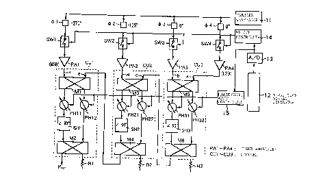
Fig. 7 is a block diagram of a construction of an
embodiment of a digital amplitude modulation amplifier
according to the present invention. In Fig. 7, the
same components as those of Fig. 2 are denoted by the
same reference symbols. In particular, the digital
amplitude modulation amplifier shown in Fig. 7 is
similar to the conventional digital amplitude
modulation amplifier shown in Fig. 2 in that it
CA 02214624 1997-09-0~
-- 19
includes carrier generator 11, modulation signal
generator 12, A/D converter 13 and on/off controller
14, and on/off controller 14 outputs a control signal
for on/off switching four switches SW1 to SW4.
Power amplifiers PA1 to PA4 having amplification
degrees weighted individually with individual bits of a
4 -bit digital signal are provided corresponding to
switches SW1 to SW4, respectively. Since a linear
characteristic is not required for power amplifiers PA1
to PA4, power amplifiers PA1 to PA4 are constructed so
as to effect a C class operation with which the power
utilization efficiency is high.
Meanwhile, the present embodiment is different
from the conventional digital amplitude modulation
. 15 amplifier in that it includes phase shift amount
controller 15 to which an output digital modulation
signal of A/D converter 13 is inputted and phase
shifters ~1 to ~ 4 to which an output carrier of
carrier generator 11 is inputted, and couplers CU1, CU2
and CU3 provided corresponding to power amplifiers PA1,
PA2 and PA3, respectively, are different in
construction from 3 dB couplers CO1 to C04 of the
conventional digital amplitude modulation amplifier.
Phase amount controller 15 is a memory to which the
digital signal is inputted as an address, and generates
a phase control signal indicative of a predetermined
CA 02214624 1997-09-0
-- 20 --
phase shift amount in response to the input address and
outputs the phase control signal to couplers CUl to
CU3.
Each of couplers CUl, CU2 and CU3 has a second
input terminal to which an output amplification carrier
of a corresponding one of power amplifiers PAl, PA2 and
PA3 is inputted, and a first input terminal to which an
output signal of coupler CU2 or CU3 of the bit of the
preceding stage (lower bit) or power amplifier PA4 is
inputted. Each of couplers CUl, CU2 and CU3 includes
first 3 dB coupler Ml, M3 or M5 for coupling input
signals to the two input terminals thereof, first
variable phase shifter PHll, PH21 or PH31 to which one
of two output signals of first 3 dB coupler Ml, M3 or
M5 is inputted, second variable phase shifter PH12,
PH22 or PH32 to which the other of the two output
signals of first 3 dB coupler Ml, M3 or M5 is inputted,
-90 degree phase shifter SHl, SH2 or SH3 for shifting
the phase of an output signal of first variable phase
shifter PHll, PH21 or PH31 by -90 degrees, and second 3
dB coupler M2, M4 or M6 for receiving and coupling
output signals of second variable phase shifter PHI2,
PH22 or PH32 and -90 degree phase shifter SHl, SH2 or
SH3. Fig. 8 is a view showing a detailed example of
coupler CUl of Fig. 7, and also the other couplers CU2
and CU3 have the same construction.
CA 02214624 1997-09-0~
A coupling output signal of second 3 dB coupler M2
in coupler CUl corresponding to the most significant
bit (MSs) is outputted as circuit output voltage EOUT
(output power POUT). It is to be noted that the phase
shift amounts of first variable phase shifters PH11,
PH21 and PH31 and second variable phase shifter PH12,
PH22 and PH32 are controlled with an output control
signal of phase shift amount controller 15.
Fig. 9(A) shows a circuit diagram of an example of
first and second variable phase shifters PH11 to PH32
of couplers CUl to CU3. As shown in Fig. 9(A),
variable phase shifters PHll to PH32 have a ~
structure including transmission line 31 inserted in
series in a signal line and a plurality of series
circuits connected in parallel between the signal line
and a reference voltage (ground) at the opposite ends
of transmission line 31 and composed of impedance
elements Zl to Z6 and switch elements Sl to S6 paired -
with each other. Switch elements S1 to S6 are
selectively switched on or off with an output control
signal of phase shift amount controller 15 shown in
Fig. 7.
By the way, if, for example, capacitors Cl and C2
which are capacitance elements are interposed as
impedance elements in the line as seen in Fig. 9(B),
then reflected waves are produced. However, if the
CA 02214624 1997-09-0
- 22 -
length of transmission line 31 inserted in series is
selected so that the reflected waves from capacitors C1
and C2 as viewed from the input end may have a phase
difference of 180 degrees relative to each other, the
reflected waves can cancel each other to suppress the
reflection (VSWR). In this instance, if capacitors are
used, then the reflected waves exhibit phase delays,
but if coils which are inductance elements are used,
then the reflected waves exhibit phase leads. For
variable phase shifters PHll and PH12 shown in Fig. 8,
the structure of Fig. 9(B) described above is used such
that output signals of the two variable phase shifters
PHll and PH12 may have a same phase by the control of
the phase shift amounts of two variable phase shifters
PHll and PH12.
Next, operation of the embodiment shown in Fig. 7
is described with reference to Figs. 7 to 9(B).
Referring to Fig. 7, a carrier of a predetermined
frequency generated by carrier generator 11 is first
shifted in phase by predetermined angles of -270
degrees, -135 degrees, 0 degree and 0 degree by phase
shifters ~ 2, ~3 and ~4, respectively, and then
supplied to and power amplified by power amplifiers
PAl, PA2, PA3 and PA4, respectively. As a requirement
for each of couplers CUl to CU3 to output an output
signal which is a coupled signal of two input signals
CA 02214624 1997-09-0~
thereto as hereinafter described, it is required that
the two input signals have the same phase, and phase
shifters ~ 2, ~3 and ~4 are provided in order to
satisfy the requirement. It is to be noted that no
coupler need be provided for phase shifters ~3 and ~4
since the phase shift amounts of them are 0 degree.
Output signals f, d and b of power amplifiers PAl,
PA2 and PA3 are supplied to first 3 dB couplers Ml, M3
and M5 in couplers CU1, CU2 and CU3 provided
corresponding thereto and are coupled to output signals
e and c of couplers CU2 and CU3 of the preceding stage
bits (lower bits) and output signal a of power
amplifier PA4 of the least significant bit (LSB) by
first 3 dB couplers Ml, M3 and M5, respectively.
Since couplers CUl, CU2 and CU3 have the same
construction, coupler CU1 is described as a
representative of them with reference to Fig. 8. When
input voltage E1 (signal e) and input signal E2 (signal
f) are inputted in the same phase (0 degree) from the
two input terminals in Fig. 8, voltages of an equal
amplitude indicated by vectors g and h are outputted to
the two output terminals of first 3 dB coupler M1. The
phases of the output voltages vary as given by the
following expressions depending upon the amplitude
ratio between voltages El and E2:
-
CA 02214624 1997-09-05
-- 24 --
El E2 ~E,2+E2 E2
E, ~_9OO+ E2 ,0O IE, +E2 ,(_~ lE,) A ~
~E,2+E22 0 -lEz ~ -lE,
where A= ~ x ----tan E ~ Y = ~n E2
The output voltages indicated by vectors h and g
given above are adjusted in phase angle to -4s degrees
as given by the following expressions as the phases
thereof are controlled by -{(y - x )/2} and +{(y
x )/2} by phase shifters PHll and PH12, respectively,
so that they may be same as each other:
( ~- ~) E '-tan ~E'+tan~'E2 tan~lE2+tan'E'
Y 2 =-~n-~E'- E~ ~ E, tan~~E2+tan~~
A signal outputted from phase shifter PHll
described above and having a phase of -45 degrees of a
vector denoted by j in Fig. 8 is further shifted in
phase by -90 degrees by phase shifter SHl so that a
signal having a phase of -135 degrees as indicated by
CA 02214624 1997-09-0
-- 25 -
vector k is obtained.
The signal outputted from phase shifter PH12 and
having the phase of -45 degrees indicated by vector i
in Fig. 8 and the signal outputted from phase shifter
SH1 and having the phase of -135 degrees indicated by
vector k in Fig. 8 are inputted as two input signals
having an equal amplitude and having a phase difference
of 90 degrees to the two input terminals of second 3 dB
coupler M2. Second 3 dB coupler M2 couples the two
input signals and outputs output voltage EOUT and dummy
voltage EDUM represented by the following expressions
and having vectors indicated in Fig. 8 to the two
output terminals thereof:
E~ 135~+ ~ ~(-45~-90~)= ~ A~-135~=~EI+Ez2 ~-135~
ED~ = ~ ~ - 45~+ ~ ~(-135~-90~)= ~ ~-45~+ ~ ~-225~=0
As can be seen from the expressions above, all
voltages El and E2 are outputted as output voltage EOUT
while dummy voltage EDUM to be outputted to the dummy
output terminal is reduced to zero (no signal is led
out).
In this manner, in Fig. 8, as two input signals
are applied in the same phase to first 3 dB coupler Ml
and the two output signals of first 3 dB coupler M1 are
CA 02214624 1997-09-0
- 26 -
controlled by phase shifters PHll and PH12 so that they
may have a same phase and besides the two input signals
to be inputted to second 3 dB coupler M2 are controlled
by phase shifter SH1 so that they may have a phase
difference of 90 degrees from each other and the input
signals controlled in this manner are inputted to
second 3 dB coupler M2, dummy voltage EDUM is reduced
to zero and the two signals inputted are all led out as
output voltage EOUT. It is to be noted that the phase
of output voltage EOUT in this instance is different by
-135 degrees from those of input signals El and E2 and
is fixed irrespective of the levels of input voltages
El and E2.
Here, when the amplitudes of two input signals e
and f are different from each other, the amplitudes of
the two signals (indicated by vectors g and h in Fig.
8) outputted from first 3 dB coupler Ml are equal to
each other, but the phases of them are different from
each other. Those signals are controlled by phase
shifters PHll and PH12 so that they may have a same
phase. A circuit of the construction of Fig. 9
described hereinabove is used for phase shifters PHll
and PH12, and a method of obtaining same phase signals
using phase shifters PHll and PH12 is described below.
In this instance, in order to simplify the control
of the phase shift amounts of phase shifters PHll and
CA 02214624 1997-09-
- 27 -
PH12, a tolerance of 90 + 18 degrees is set for the
phase difference between the input signals to each of
phase shifters PHll and PH12, and the phases are
controlled stepwise. It is to be noted that the loss
originating from a phase error of +18 degrees is 2.3 %
in the maximum and can be ignored.
In order that the conditions described above may
be satisfied, the the power ratio relationships between
powers E and F of input signals e and f, the phase
difference between the two signals (indicated by
vectors g and h in Fig. 8) outputted from first 3 dB
coupler M1, the phase shift control amounts of phase
shifters PHll and PH12 by phase shift amount controller
15 and the phase difference between the two signals
(indicated by vectors i and k in Fig. 8) inputted to
second 3 dB coupler M2 is set in such a manner as
illustrated, for example, in a table of Fig. 10. The
reason why the phase difference between the two signals
(indicated by vectors g and h in Fig. 8) outputted from
first 3 dB coupler M1 is classified in ranges of 18
degrees in Fig. 10 is that it is intended to simplify
the phase control (however, an error of 2 to 3 % is
permitted~. Further, in Fig. 10, voltage ratios are
squared to convert them into power ratios.
As can be seen from Fig. 10, since states of the
two input signals are limited to several combinations,
CA 022l4624 l997-09-0
- 28 -
phase shift amount control for all angles over 360
degrees is not required, but a step phase shifter which
can provide phase shift amounts of +36, 0, -g, -18, -27
and -36 degrees may be used for phase shifter PH11
while another step phase shifter which can provide
phase shift amounts of -36, 0, +9, +18, +27 and +36
degrees may be used. It is to be noted that the basic
phase shift amounts in Fig. 10 are represented by -{(y
- x )/2} and +{(y - x )/2} given hereinabove.
Phase shifters PHll and PH12 which realize the
phase shift amounts described above are shown in Figs.
ll(A) and ll(B), respectively. Each of phase shifters
PHll and PH12 has a ~ structure including transmission
line 31 inserted in series in a signal line and
capacitors or coils interposed between the signal line
and a reference voltage (ground) at the opposite ends
of transmission line 31. Switch elements Sll to S20 or
S21 to S30 which are selectively switched on or off by
an output control signal of phase shift amount
controller 15 shown in Fig. 7 are connected in series
to the corresponding capacitors or coils between the
capacitors or coils and the reference voltage (ground).
In order to obtain a phase delay, a switch element
is controlled to an on-state so that a capacitor may be
connected to the input terminal and the output terminal
of transmission line 31, but in order to obtain a phase
CA 02214624 1997-09-0
- 29 -
lead, another switch element is controlled to an on-
state so that a coil may be connected to the input
terminal and the output terminal of transmission line
31. In Figs. ll(A) and ll(B), each numerical value
represents a phase shift amount to be obtained, and
associated arrow marks indicate switch elements to be
switched on in order to obtain the phase shift amount.
It is to be noted that, in order to obtain the phase
shift amount of 0 degree, all of switch elements Sll to
S20 and S21 to S30 are opened (off). Consequently, a
signal passes only through transmission line 31, and
the phase shifter exhibits a through-state and the
phase shift amount of 0 degree is obtained.
The output amplification signals of power
amplifiers PA4 and PA3 are controlled by coupler CU3 so
that the phase difference between them may be 90
degrees as they are inputted as signals a and b in a
same phase to and coupled by first first 3 dB coupler
M5 and the two output signals of first 3 dB coupler M5
are phase shifted by variable phase shifters PH31 and
PH32 so that they may have the same phase and then the
output signal of variable phase shifter PH31 is phase
shifted by -90 degrees, and the output amplification
signals controlled in this manner are inputted to
second variable 3 dB coupler M6. Consequently, two
input signals a and b inputted are all led out as an
..... . .
CA 02214624 1997-09-0
- 30 -
output voltage and inputted as signal c to first
variable 3 DB coupler M5 of coupler CU2.
Here, since output voltage c of coupler CU3
inputted to one of the two input terminals of first 3
dB coupler M3 in coupler CU2 is displaced by -135
degrees from input signals a and b, it is phase shifted
by -135 degrees by phase shifter ~2 and inputted to
first 3 dB coupler M3 so that signal d to be inputted
to the other input terminal of first 3 dB coupler M3
through switch SW2 and power amplifier PA2 may have a
same phase as signal c. Thus, two input signals c and
d are coupled by first 3 dB coupler M3. The two output
signals of first 3 dB coupler M3 are controlled in
phase by variable phase shifters PH21 and PH22 so that
they may have a same phase and the output signal of
phase shifter PH1 is phase shifted by -90 degrees by
phase shifter SH2 so that the two output signals of
first 3 dB coupler M3 are controlled so as to have a
phase difference of 90 degrees and inputted to second 3
dB coupler M4 in this state. Then, the two signals are
coupled by second 3dB coupler M4 so that they are all
outputted as an output voltage from second 3 dB coupler
M4 and inputted as signal e to first 3 dB coupler M1 of
coupler CU1.
Since output voltage e of coupler CU2 inputted to
one of the two input terminals of first 3 dB coupler Ml
CA 02214624 1997-09-0~
in coupler CUl is displaced by -135 degrees from input
signals c and d (by -270 degrees from signals a and b),
- it is phase shifted by -270 degrees in advance by phase
shifter ~1 so that signal f to be inputted to the
other input terminal of first 3 dB coupler M1 through
switch SW1 and power amplifier PA1 may have the same
phase as signal e, and output voltage e phase shifted
in this manner is inputted to coupler CUl. Those input
signals e and f are coupled by coupler CU1, from which
two signals e and f inputted are all led out as output
voltage EOUT while dummy voltage EDUM is reduced to
zero.
Switches SW1 to SW4 of the digital amplitude
modulation amplifier shown in Fig. 7 exhibit totaling
16 (= 24) combinations of on/off states in response to
different levels of the modulation signal, and input
signal powers of couplers CUl to CU3 and power ratios
between them and phase shift amounts of first variable
phase shifters PH11 to PH31 and second variable phase
shifters PH12 to PH32 in the 15 combinations of on/off
states except the combination of off states of all of
switches SWl to SW4 are collectively illustrated in a
table of Fig. 12. Referring to Fig. 12, A, B, C, D, E
and F represent the powers of input signals a, b, c, d,
e and f, respectively, and when any of power amplifiers
PAl to PA4 is "1", this represents that a corresponding
CA 02214624 1997-09-0
- 32 -
one of switches SWl to SW4 provided corresponding to
power amplifiers PAl to PA4, respectively, is on and
that one of power amplifiers PAl to PA4 has an input
and an output.
Fig. 13 is a table illustrating the relationship
of the input modulation signal level of the digital
amplitude modulation amplifier shown in Fig. 7 to input
power PIN, output power POUT and loss LOSS in the 15
combinations of on/off states of switches SWl to SW4
described above. Here, the input modulation signal
level is denoted by INPUT, and input power PIN is a
total power of input signals a, b, c and d. Meanwhile,
output power POUT represents the output power of the
output terminal of coupler CUl.
As apparent from Fig. 13, the loss power (LOSS)
which is absorbed by dummy resistors R1 to R3 of
couplers CU1 to CU3 is lower than 0.2 dB and is reduced
remarkably from that of the conventional digital
amplitude modulation amplifier. The loss power can be
further reduced by increasing the variable step widths
of the phase shift amounts of phase shifters PH11 to
PH32.
Next, a second embodiment of the present invention
is described. Fig. 14 shows a block diagram of the
second embodiment of the digital amplitude modulation
amplifier according to the present invention. In Fig.
CA 02214624 1997-09-0~
-
14, the same components as those of Fig. 7 are denoted
by the same reference symbols, and overlapping
description of them is omitted here. The embodiment
shown in Fig. 14 is characterized in that a single
amplitude modulator 17 and a single A class or AB class
power amplifier 18 are provided for lower bits of an
output digital signal of A/D converter 13.
Referring to Fig. 14, a digital output signal of
A/D converter 13 is divided into upper bits and lower
bits determined in advance, and only the upper bits are
supplied to on/off controller 14 while the lower bits
are supplied to D/A converter 16 and converted into an
analog signal by D/A converter 16. Here, the upper
bits and the lower bits are determined arbitrarily.
Here, for simplified description, it is assumed, as an
example, that the digital signal has 4 bits and 1 bit
is used as the lower bits while the other 3 bits are
used as the upper bits.
The output analog signal of D/A converter 16 is
supplied to amplitude modulator 17, by which a carrier
from carrier generator 11 inputted thereto through
phase shifter ~4 is amplitude modulated in an analog
fashion with the inputted output analog signal. The
amplitude modulated wave obtained by amplitude
modulator 17 and corresponding to the lower bit is
first power amplified by A class or AB class liner
CA 02214624 1997-09-0
-- 34 --
power amplifier 18 and then inputted to coupler CU1, by
which it is coupled to (power amplified with) an output
signal corresponding to the upper bit of power
amplifier PAl.
Accordingly, in the present embodiment, the lower
bits are replaced by one class power amplifier 18.
While 1 bit is used as the lower bits for simplified
illustration in Fig. 14, if it is assumed otherwise
that the digital signal has 8 bits and the lower bits
are 3 bits while the upper bits are 5 bits, then a
digital amplitude modulation amplifier can be formed
from five power amplifiers PA and five couplers and one
A class or AB class power amplifier 18.
Therefore, while, in the first embodiment wherein
a number of power amplifiers equal to the number of
bits of the digital signal must be prepared, the number
of power amplifiers increases as the number of bits
increases, the present embodiment has an advantage in
that, even if the number of bits of the digital signal
increases, it can be formed using a number of power
amplifiers smaller than that of the first embodiment.
Fig. 15 shows a diagrammatic view of a concept of
composition of an output amplitude modulated wave of
the second embodiment shown in Fig. 14. In Fig. 15,
pal to pa3 denote output signal components of power
amplifiers PAl to PA3 corresponding to the upper bits
CA 02214624 1997-09-0~
in the output amplitude modulated wave, and slanting
line portion paO indicates an analog amplitude
modulated wave component corresponding to the lower
bits.
Although use of A class or AB class power
amplifier 18 deteriorates the power utilization
efficiency, since the signal level corresponding to the
lower bit is very low comparing with those of the upper
bits as seen from Fig. 15, the deterioration of the
efficiency by the lower bits does not have a much
influence upon the efficiency of the entire amplifier.
Further, the envelopes of the amplitude modulated wave
become smooth and also production of harmonics can be
reduced.
Next, a third embodiment of the present invention
is described. Fig. 16(A) shows a block diagram of the
third embodiment of the digital amplitude modulation
amplifier according to the present invention. As shown
in Fig. 16(A), the digital amplitude modulation
amplifier includes phase modulated carrier generator
21, modulation signal generator 22 and digital
amplitude modulation amplification element 23. Digital
amplitude modulation amplification element 23 has a
circuit construction of one of the embodiments of the
present invention shown in Figs. 7 and 14 except
carrier generator 11 and modulation signal generator
CA 02214624 1997-09-0
-- 36 --
12.
In other words, the present third embodiment
includes, in place of carrier generator 11 of the first
or second embodiment, phase modulated carrier generator
21 which receives, as input signals to the power
amplifiers corresponding to the individual bits, a
carrier phase modulated with an information signal
different from the modulation signal of modulation
signal generator 22 so that a modulated wave which is
modulated in both amplitude and phase can be obtained.
With the present third embodiment, since a phase
modulated carrier can be amplitude modulated, a single
side band (SSB) signal can be obtained by amplitude
modulating a carrier phase modulated with phase
information ~ with a modulation signal having
amplitude information r and represented by Vm cos~mt
as seen in Fig. 16(B). Further, a vestigial side band
(VSB) signal represented by a vector which draws an
elliptical locus can be obtained by amplitude
modulating a carrier phase modulated with phase
information a with modulation signal Vml cos~mlt or
Vm2 cos~m2t having amplitude information r as seen
from Fig. 16 (C) .
It is to be noted that the present invention is
not limited to the embodiments described above. For
example, while, in Fig. 7, the number of couplers is 3
CA 02214624 1997-09-0~
including couplers CUl to CU3 and the number of power
amplifiers is 4 including power amplifiers PAl to PA4,
the number of couplers may be an arbitrary number N
corresponding to a quantization bit number of a digital
signal while the number of C class power amplifiers may
be (N + 1). Meanwhile, in the embodiment of Fig. 14,
if the number of the lower bits is m, then the
amplifier can be constructed using (N + 1 - m) C class
power amplifiers PA and one A class or AB class power
amplifier 18.
As described above, according to the present
invention, where a plurality of C class power
amplifiers which exhibit a high power utilization
efficiency are used and output signals of the power
amplifiers are composed using couplers, since the power
loss absorbed by dummy loads to the couplers can be
substantially eliminated, a digital amplitude
modulation amplifier which is higher in power
utilization efficiency than conventional digital
amplitude modulation amplifiers and regenerates the
amplitude of an input modulation signal with a high
degree of fidelity.
Further, according to the present invention, since
power amplifiers which are provided corresponding to
the upper bits of a digital signal and effect a C class
operation are used while a single A class or AB class
.... .... .
CA 02214624 1997-09-0
- 38 -
power amplifier is used commonly for the lower bits of
the digital signal, also where the number of bits of
the digital signal is large, the digital amplitude
modulation amplifier can be formed in a simple
construction.
Further, according to the present invention, if an
input carrier is phase modulated with a desired
information signal in advance, since a modulated wave
which includes both of amplitude information and phase
information can be outputted, a digital amplitude
modulation amplifier having a high universality can be
realized.
Next, embodiments of a television broadcasting
machine of the present invention are described with
reference to the drawings.
Fig. 17 shows a block diagram of a television
broadcasting machine of a fourth embodiment of the
present invention. Referring to Fig. 17, an analog
video signal inputted via input terminal 101 is
converted into a digital signal by A/D converter 102
and then inverted by signal invertor 103, whereafter it
is inputted to first finite impulse response (FIR)
digital filter 104 and second finite impulse response
(FIR) digital filter 105.
First FIR digital filter 104 has a frequency
characteristic, for example, as shown in Fig. 18(A)
CA 02214624 1997-09-0
- 39 -
such that it passes therethrough signal components of a
band which makes the DSB part of a VSB signal and
limits the amplitude of signal components of another
band which makes the SSB part to 1/2 time. In Fig.
18(A), frequency components lower than 0.75 MHz are
signal components of the band which makes the DSB part
of a VSB signal, and frequency components from 0.75 MHz
to 4.2 MHz are signal components of the band which
makes the SSB part. From this first FIR digital filter
104, I information 106 is extracted.
Meanwhile, second FIR digital filter 105 has such
a frequency characteristic, for example, illustrated in
Fig. 18(B) that it passes therethrough only signal
components of a band which makes the SSB part of a VSB
signal with an amplitude equal to 1/2 that of the input
thereto and the phase of the output signal thereof is
displaced by 90 degrees from that of the output signal
of first FIR digital filter 104. In Fig. 18(B), signal
components from 0.75 MHz to 4.2 MHz are signal
components of a band which makes an SSB. From this
second FIR digital filter 105, Q information 107 is
extracted.
Impulse responses for calculation of coefficients
of those FIR digital filters 104 and 105 are given by
the expressions given below. Here, N represents the
tap coefficients of FIR digital filters 104 and 105,
... . . . . .
CA 02214624 1997-09-0
- 40 -
and in order to satisfy the specifications for a
television signal, 128 taps or more are required.
1 N-l
First FIR digital filter 4: h (n)=N~H~k)cos{2~n(k-L)lN}
l N-l
Second FIR digital filter 5: h (n)=N~H(k)sin{27m(k--L)/N}
Transmission function H(k) is given asymmetrically with
respect to angular frequency ~ = 0 as given by the
following expression:
1(-0.75MHz<k<+4.2MHz)
H(k)=~
O(k~-0.75MHz,k~+4.2MHz)
An example of the amplitude-frequency
characteristic of first FIR digital filter 104
described above is illustrated in Fig. l9(A), and an
example of the phase-frequency characteristic is
illustrated in Fig. l9(B). Meanwhile, an example of
the amplitude-frequency characteristic of second FIR
digital filter 105 is illustrated in Fig. l9(C), and an
example of the phase-frequency characteristic is
illustrated in Fig. l9(D).
I information 106 and Q information 107 output~ed
from FIR digital filters 104 and 105 described above
are inputted, as seen in Fig. 17, to polar coordinate
CA 02214624 1997-09-0
- 41 --
transformation circuit 108, by which they are converted
into amplitude information A(t) and phase information
U(t). The relationship of I information 106 and Q
information 107 to amplitude information A(t) and phase
information ~(t) is such as illustrated in Fig. 20.
Referring back to Fig. 17, of amplitude
information A(t) and phase information ~(t) extracted
from polar coordinate transformation circuit 108,
amplitude information A(t) is supplied to amplitude
control circuit 115 while phase information ~(t) is
supplied to phase modulator 111, by which a carrier
inputted from carrier generator 112 is converted into a
phase modulated wave by phase modulation with phase
information ~(t). The phase modulated wave is
supplied to D/A converter 113, by which it is converted
into an analog signal. Then, unnecessary high
frequency components are removed from the analog signal
by low-pass filter (LP~) 114, and a resulting signal is
supplied to power amplifier 116.
While power amplifier 116 power amplifies and
outputs the phase modulated wave inputted thereto
through LPF 114, the output amplitude level is
controlled with the amplitude control signal inputted
from amplitude control circuit 115 and corresponding to
amplitude information A(t). Consequently, a signal
produced by amplitude modulation of the phase modulated
CA 02214624 1997-09-0
- 42 -
wave with the amplitude control signal, that is, a
vestigial side band (VSB) signal, is outputted to
output terminal 117. In this manner, a VSB signal can
be obtained without using a vestigial side band filter.
It is to be noted that, as an example of a method
of controlling the amplitude level of power amplifier
116, there is a method wherein, as shown in Fig. 21 (A),
the drain of field effect transistor (FET) 121, which
is an amplification element, is connected to an output
terminal of amplitude control circuit 115 via coil 122
so that the drain voltage of FET 121 iS controlled with
an output voltage of amplitude control circuit 115 to
vary the drain output voltage.
Meanwhile, Fig. 21 ( B) shows another example
wherein, in place of FET 121, bipolar transistor (NPN
transistor) 123 iS used as an amplification element.
In this example, the collector voltage of bipolar
transistor 123 can be varied by controlling the same
with an output voltage of amplitude control circuit 115
via coil 124.
Next, a fifth embodiment of the present invention
is described. Fig. 22 shows a block diagram of a
television broadcasting machine of the fifth embodiment
of the present invention. In Fig. 22, same components
as those of Fig. 17 are denoted by same reference
symbols, and overlapping description thereof is omitted
CA 02214624 1997-09-0
- 43 -
here. Referring to Fig. 22, an input analog signal
inverted by signal invertor 103 is inputted to low-pass
filter (LPF) 133 and band-pass filter (BPF) 134 after a
dc voltage from dc voltage source 132 iS added to it by
adder 131.
LPF 133 passes therethrough only signal components
(lower than 0. 75 MHz) of a band which makes the DSB
part of a VSB signal. Meanwhile, BPF 134 passes
therethrough only signal components (0. 75 MHz to 4.2
MHz) of another band which makes the SSB part of the
VSB signal. An output signal of BPF 134 is reduced to
1/2 in amplitude by 1/2 attenuator 135 and then added
to an output signal of LPF 133 by adder 136 to form I
information. Meanwhile, the output of 1/2 attenuator
135 is supplied also to Hilbert transformer 137, by
which it is phase shifted by 90 degrees to form Q
information.
The I information and the Q information mentioned
above are supplied to analog polar coordinate
transformer 138, by which they are converted into
amplitude information r (= (12 + Q2) 1/2 ~ and phase
information ~ (= tan~l(Q/I)). Here, analog polar
coordinate transformer 138 is composed of, as seen in
Fig. 23, multipliers 141 and 142, trigonometric
function operator 143, adder 144 and square root
operator 145. Referring to Fig. 23, a signal obtained
CA 02214624 1997-09-0~
-
- 44 -
by squaring input I information by multiplier 141 and
another signal obtained by squaring input Q information
by multiplier 142 are first added by adder 144 and then
supplied to and square root operated by square root
operator 145. Consequently, amplitude information r
represented by (I2 + Q2)1/2 is outputted from square
root operator 145.
Meanwhile, trigonometric function operator 143
receives the input I information and the input Q
information, performs operation of tan~1(Q/I) and
outputs a result of the calculation as phase
information ~. Multipliers 141 and 142, trigonometric
function operator 143 and square root operator 145 can
be realized using a linear IC or a like device.
Of amplitude information r and phase information
~ outputted from analog polar coordinate transformer
138, amplitude information r is supplied, similarly as
in the fourth embodiment, to amplitude control circuit
115 while phase information ~ is supplied to phase
modulator 111, by which a carrier from carrier
generator 112 is phase modulated with phase information
~. The phase modulated wave from phase modulator 111
is supplied to power amplifier 116, by which it is
amplitude modulated with a control signal from
amplitude control circuit 115. Consequently, a VSB
signal is obtained from power amplifier 116.
CA 02214624 1997-09-0
- 45 -
With the present embodiment, amplitude information
and phase information can be detected from a video
signal using an analog circuit, and a VSB signal can be
obtained from the amplitude information and the phase
information without using a vestigial side band filter.
As described above, according to the present
invention, since a carrier is phase modulated and
amplitude modulated with amplitude information and
phase information obtained from an input video signal,
a vestigial side band signal can be obtained without
using vestigial side band. Consequently, a television
broadcasting machine can be constructed at a reduced
cost comparing with a conventional television
broadcasting machine which employs a vestigial side
band filter.