Note : Les descriptions sont présentées dans la langue officielle dans laquelle elles ont été soumises.
CA 02214927 1997-10-31
Patent name: Methods for making phase masks with spatial variable f~lrst
order ef~lciency for ~Iber Bragg grating fabrication
Background:
UV light can induce a permanent refractive index change in some kind optical fibers and
optical wave guides. The photosensitivity of the certain kind optical fiber waveguide can
be used to make Bragg gratings, which is a permanent, spatially periodic refractive index
modulation along the length of the photosensitive core of the optical fiber or optical wave
guide. Fiber Bragg gratings have many applications in optical fiber telecommunication,
optical sensor and optical information process. Fiber Bragg gratings can be used as
bandpass reflective filters, dense wavelength division multiplexing(DWDM) add and
drop filters, dispersion compensation, and optical fiber sensors.
There are two methods of side writing Bragg gratings in optical fiber and optical wave
guide, one of them is holography approach and another one is phase mask approach.
Holography approach is using two beam interference to form a periodic light intensity
modulation along optical fiber or optical wave guide. The period of the pattern is
controlled by controlling the angle between the interfering beams. Holography approach
is described in U.S. patent application Ser. No. 4,474,427 invented by K.O.Hill,
B.S.Kavassaki, D.C. Johnson, and Yoshimassa Fujii and in U.S. patent application Ser.
No. 4,807,950 invented by Glenn et al. Phase mask method is the most common way to
fabricate Bragg grating in optical fiber and optical wave guide. A phase mask is an
uniform or chirped grating in fused silica glass substrate. Optical fibers or optical wave
guide is placed close or near close under phase mask. When a UV light illuminates the
phase mask, +l and -I diffraction orders of the grating in phase mask will interference
each other along the fiber or wave guide core and a refractive index change in optical
fiber or optical wave guide is formed. Phase mask method is very robust and insensitive
to the environment conditions such as vibration. Phase mask method of fabricating such
Bragg gratings is described in U.S. patent application Ser. No. 969,774 invented by
K.O.Hill, B.Malo, F.Bilodeau and D. Johnson and entitled METHOD OF
FABRICATING BRAGG GRATINGS USING A SILICA GLASS PHASE GRATINGS
MASK.
Phase masks can be made by holography approach or by electron beam direct write
approach. To make a phase mask by holography approach is very similar as writing a
grating on optical fiber. First two interference beams are used to form a sinusoid intensity
modulation on a layer of photoresist coated on a fused silica glass substrate. After
developing a sinusoid profile on the photoresist layer is formed. Then a dry etching is
implemented to transfer the sinusoid profile on the photoresist into the fused silica glass
substrate underneath to make a phase mask. The another method to make phase masks is
using electron beam lithography machine to write very fine lines on a photoresist layer on
the top of a Chromium layer with fused silica glass substrate plate. After developing a
very fine pattern on the photoresist layer is formed. The open Chromium on the
photoresist pattern layer is removed by a wet etching process and the left photoresist is
cleaned to get a Chromium pattern on the fused silica glass substrate. A dry etching
CA 02214927 1997-10-31
process is used to transfer the fine line patterns into fused silica glass substrate to make a
phase mask. The electron beam direct write approach is a standard photomask making
process in microelectronic industry and t'ollowed by a dry etching process.
Fiber Bragg gratings written by a phase mask with an uniform speed laser scanning will
have a main peak in the center reflection spectrum accompanied by a series of side lobes
at adjacent wavelengths. It is very important to lower the reflectivity of these side lobes
or 'apodise' the reflection spectrum of the fiber Bragg grating in these optical fiber
devices where high rejection of the nonresonant light is required. DWDM systems
require device that can isolate channels that are spaced by only lOOGHz(0.8nm at1~50nm wavelength). Fiber Bragg gratings are the promise components in the DWDM
systems as optical signal channel adder( input channel ) and optical signal channel
dropper( output channel ). For example that one optical wavelength channel will be
dropped from optical fiber should have no effect on other optical wavelength channels.
A high main peak in the center wavelength reflection spectrum with very low side lobes
at adjacent wavelengths is very important for DWDM fiber Bragg gratings.(reference 1)
Another benefit of the reflection spectrum apodisation of fiber Bragg gratings is the
improvement of the dispersion compensation characteristics of chirped Bragg gratings.
(reference 2)
Both holographic approa~h and phase mask approach can make apodised fiber Bragg
gratings. The holographic approach uses two laser beams with intensity variation from
beam center to the beam edge (for example Gaussian beam intensity profile) to write
fiber Bragg gratings. The two laser beams will make an intensity modulation grating
along the fiber cc re so the apodised fiber Bragg grating was made. This kind apodised
fiber Bragg grating is not "pure apodisation" since not only the refractive index grating
modulation is apodised but also the average induced refractive index is not constant and
has a spatial profile along the fiber core. This kind apodisation approach can suppress the
side lobes in the spectral response of the fiber Bragg gratings. But the fiber Bragg
gratings will have a fine structure on the short wavelength side of their reflection
response curve which is particularly strong in high reflectivity gratings.(reference 3)
Phase mask approach can also make spodised fiber Bragg gratings by varying exposure
time(varying scanning speed) along the length of the fiber Bragg grating. A longer
exposure time(slower scanning speed) can induce a larger local refractive index
modulation grating and a short exposure time(faster scanning speed) will induce a small
local refractive index modulation grating. The apodised fiber Bragg gratings made with
this approach will have the same problem as holographic approach does: not only
refractive index is modulated but also the average induced refractive index varies along
the fiber Bragg grating length. The same problem mentioned above, the fine structure on
the short wavelength side of the grating reflection spectrum, will occur with the apodised
fiber Bragg gratings made by the phase mask approach.
.1. Albert, K.O.Hill, B.Malo, S. Theriault, F. Bilodeau, D.C.Johnson and L.E.Erickson
pror~osed using a phase mask with variable dift'raction efficiency to make a fiber Bragg
grating with apodisation of the spectral response. They made a phase mask with variable
grating groove size (groove width and or groove depth in the grating period) to varying
CA 02214927 1997-10-31
the relative intensity of the first order diffraction beams. When a UV laser beam is
scanning the phase mask with variable local first order diffraction efficiency the
interferent pattern modulation varies along the fiber Bragg grating length. Since the
exposure time is the same(uniform scanning speed) the average induced refractive index
along the fiber Bragg grating length will be constant. This method can make a fiber
Bragg grating with "pure apodisation" with only refractive index grating modulation
change and the constant average induced refractive index. They used focused ion beam
machine to make this kind phase masks. It is not practical to make a long phase mask
with focused ion beam machine because it will take very long writing time for focused
ion beam machine to make a phase mask with a size of lOmm x 3 mm.
~ I.Singh, and W.W.Morey also made apodised fiber Bragg gratings for DWDM using a
variable efficiency phase mask.(reference 4) The basis of their variable efficiency phase
mask is by varying the grating groove depth to change the first order diffraction
efficiencies, as same as that proposed by J. Albert et al.. But the method to make the
variable efficiency phase mask is different from the focused ion beam machine method
used by J. Albert et al.. The variable efficiency phase mask is made by holography
approach with a interference from two beams that have a spatially variable intensity
profile such as Gaussian beam profile. But the holographic approach have some
disadvantages such as: not easy to control the interference beam spatial intensity profile,
not easy to make chirped phase mask with variable efficiency.
Invention
In the present invention two new methods of making apodised phase masks, which have
spatial variable grating groove depth to get variable first order efficiency along the
grating length, are presented.
1. Method one:
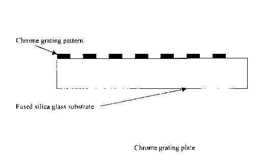
A chrome photomask of grating patterns is made first by an electron beam direct write
lithography machine. The chrome photomask made on a fused silica plate has many
grating patterns inside. Then the chrome photomask is cut into several plates with each
one of them contains a grating patterns.(see figure 1) After cleaning the chrome grating
plates a photoresist layer is coated on the chrome grating plates.(see figure 2) A gray
level mask with spatial variable optical transmission is used in a lithography process to
form a spatial variable photoresist thickness on the chrome grating plate along the grating
length.(see figure 3) The lithography process can be implemented with a contact mask
aligner lithography machine or with a project image reduction lithography machine called
"stepper" in microelectronic industry. The gray level mask with the spatial variable
optical transmission profile is put on the mask position in the lithography machine and
the chrome grating plate coated with a photoresist layer is put in the wafer position in the
lithography machine. After the exposed photoresist on the chrome grating plate is
developed a spatial variable thickness profile on the photoresist layer is made.(see figure
4) A dry etching process is followed to transform the photoresist profile into the fused
silica plate to make a phase mask with spatial groove depth profile.(see figure 5) The
chrome grating pattern is used as protect mask during the dry etching process so only
open area without chrome in the grating pattern will be etched down into substrate. Since
there is a spatial variable photoresist profile on the top of the chrome grating plate, the
w~
CA 02214927 1997-10-31
local grating groove depth on the substrate, where the photoresist is thicker, will be
shallow and the local grating groove depth, where the photoresist is thinner, will be
deeper.(see figure 6) Since the grating groove depth on the substrate varies along the
phase mask length the first order efficiency changes also along the phase mask length.
The fiber Bragg gratings made by the phase mask with spatial variable first order
efficiency will have a main reflection peak of the center wavelength with suppressed side
lobes: apodised reflection spectrum. By carefully designing the grating groove depth
profile along the grating length the phase mask can make fiber Bragg gratings with
Gaussian apodisation or other kind apodisation profile in the reflection spectrum.
In the invention the grating patterns in the chrome photomasks made by electron beam
lithography approach are uniform gratings or chirped gratings. The grating periods in the
chrome photomask can be from 0.5 micro meter to 1.2 micrometers, which are
corresponding to working wavelengths from 0.85 micrometer to 1.55 micrometers. To be
illuminated by UV laser beam the chrome photomasks are made on fused silica glass
plates. One chrome photomask can contain one or several grating patterns. If the chrome
photomask contains several grating patterns the chrome photomask can be diced into
several plate pieces, each of them contains one grating pattern. After the chrome grating
plates are cleaned they are coated with a photoresist layer. A prebake process is followed
and the chrome grating plates with the photoresist layer are put into an oven or put on a
hot plate for a certain time. Then a lithography process is implemented to transform the
spatial variable optical density on a gray level mask into a spatial variable photoresist
depth profile on the chrome grating plate.
In the invention the lithography process can be implemented in a contact mask aligner
lithography machine or a projection image reduction lithography machine called
"stepper" in microelectronic industry. The chrome grating plates are put on the wafer
position in the lithography machine. A ~ray level mask with spatial variable optical
transmission is used as the mask in the lithography machine. A conventional photomask
has only two optical transmission levels: transparent(white) or not transparent(black).
Gray level masks can have more than two optical transmission levels. For example a gray
level mask have three optical transmission levels: 100% transparent(white), 50%
transparent and 0~/o transparent(black). Normally a gray level mask can have eight to
several hundred optical transmission levels. When a gray level mask with eight
transmission levels is illuminated with a uniform optical beam the optical intensity of the
output beam will be modulated with eight levels. If a chrome grating plate with a
photoresist layer is illuminated under the modulated optical beam a photoresist profile
with eight different. depths will form on the chrome grating plate after the exposed
photoresist plate is developed. Using a gray level mask with a spatial variable optical
transmission profile carefully designed a photoresist layer with the spatial variable depth
profile like Gaussian profile or other kind profiles can be obtained on a chrome grating
plate.
In the invention the gray level mask, which has a spatial variable optical transmission
profile specially designed, can be made on the high energy beam sensitive glass with
electron beam lithograr)hy machine(reference 5). The gray level mask can also be made
CA 02214927 1997-10-31
on a conventional sio2 by mean of evaporation of metal alloy such as Inconel(a nickel
chromium iron alloy) and a following liftoff step.(reference 6) The gray level mask can
also be made by changing the number or area of openings in a chrome
photomask.(reference 7) The gray level mask can also be made on the conventionalcommercial slide imagers and low-contrast film(reference 8-9).
In the invention after a spatial variable photoresist thickness layer is formed on the
chrome grating plate with a lithography process a dry etching process is implemented to
transfer the spatial photoresist profile into the fused silica glass substrate. The dry etching
process can be reactive ion etching. The dry etching process can also be a chemical
assistant ion beam etching. The etching ratio between photoresist and substrate can be
different. The photoresist etching ratio can be quicker than the substrate etching ratio.
The photoresist etching ratio can be slower than the substrate etching ratio. For different
etching ratio between the photoresist and the substrate different spatial photoresist
profiles are required to get final spatial grating groove depth profiles in the substrate.
In the invention the chrome grating pattern is used as a protection mask during the dry
etching process. Only the open area without chrome will be etched down into fused silica
substrate with the dry etching process. If there is no photoresist layer on the top of the
chrome grating pattern a grating with the same grating groove depth will be made by the
dry etching process. If there is no chrome grating pattern under the spatial variable
photoresist layer a spatial variable profile in the substrate will be made with the dry
etching process. Since there is a spatial variable photoresist profile on the top of the
chrome grating plate the etched grating groove depth will have a spatial variable profile
along the grating length. After cleaning the chrome and photoresist finally a phase mask
with a spatial variable grating groove depth profile along the grating length on the fused
silica glass substrate has been made. A phase mask with a spatial variable grating
groove depth profile will have a spatial variable first order diffraction efficiencies along
the grating length. The phase mask with a spatial variable first order efficiencies along
the grating length can make apodised fiber Bragg gratings with the main center reflective
peak and suppressed side lobes, which is very important for DWDM system to reduce the
interchannel interference.
In the invention the Bragg grating can be made in optical fiber or optical waveguide.
2. Method two:
A phase mask with uniform grating groove depth is made first. (see figure 7) Then the
phase mask is coated with a photoresist layer.(see figure 8) A gray level mask with
spatial variable optical transmission is used in a lithography process to form a spatial
variable photoresist thickness on the chrome grating plate along the grating length.(see
figure 9) The lithography process can be implemented with a contact mask alignerlithography machine or with a project image reduction lithography machine called"stepper" in microelectronic industry. The gray level mask with the spatial variable
optical transmission profile is put on the mask position in the lithography machine and
the phase mask with the uniform grating groove depth coated with a photoresist layer is
put in the wafer position in the lithography machine. After the exposed photoresist on the
CA 02214927 1997-10-31
phase mask is developed a spatial variable thickness profile on the photoresist layer is
made.(see figure 10) A dry etching process is followed to transform the photoresist
profile into the fused silica plate to make a phase mask with spatial groove depth
profile.(see figure 11) Since there is a spatial variable photoresist profile on the top of
the phase mask, the local grating groove depth on the substrate, where the photoresist is
thicker, will be shallow and the local grating groove depth, where the photoresist is
thinner, will be deeper.(see figure 12) Since the grating groove depth on the substrate
varies along the phase mask length the first order efficiency changes also along the phase
mask length. The fiber Bragg gratings made by the phase mask with spatial variable first
order ef'ficiency will have a main reflection peak of the center wavelength withsuppressed side lobes: apodised reflection spectrum. By carefully designing the grating
groove depth profile along the grating length the phase mask can make fiber Bragg
gratings with Gaussian apodisation or other kind apodisation profile in the reflection
spectrum.
CA 02214927 1997-10-31
References:
1). Matschara M. and Hill K.O., "Optical-waveguide band-rejection filters: design",
Appl. Opt., vol. l 3, pp.2886-2888(1974).
2). Hill K.O., Theriallt S., Malo B., Bilodeau F., Kitigawa T., Johnson D.C., Albert J.,
Takiguchi K., Kataoka T., and Hagimoto K., "Chirped in-fiber Bragg grting dispersion
compensators: Linearisation of dispersion characteristic and demonstration of dispersion
compensation in 100km, 10Gbit/s optical fibre link", Electron. Lett., vol. 30, ppl755-
1756( l 994)
3). Mizrahi V., and Sipe J.E., "Optical properties of photosensitive gratings", Journal of
Lightwave Technology, LT-Il, pp.823-825(1993).
4). H. Singh, and W.W.Morey, "Apodized Fiber Gratings for DWDM Using Variable
Efficiency Phase Masks", IEEE/LEOS Summer Topical Meetings, 1997, Montreal,
Canada.
5). Walter Daschner, Pin Long, Robert Stein, Chuck Wu and S.H.Lee, " General aspheric
refractive micro-optics fabricated by optical lithography using a high energy beam
sensitive glass gray-level mask", Journal of Vacuum Science and Technology B, vol.
14(6), pp. 3730-3733(1996).
6). Walter Daschner, Pin Long, Michael Larsson, and S.H.Lee, " Fabrication of
diffractive optical elements using a single optical exposure with a gray level mask",
Journal of Vacuum Science and Technology B, vol. 13(6), pp.2729-2731 (1995).
7). Y.Opplinger, P.Sixt, J.M.Stauffer, J.M.Mayor, P.Regnault and G.Voirin"One-step 3D
Shaping Using a Gray-Tone Mask for Optical and Microelectronic Applications",
Microelectronic Engineering, Vol. 23, pp.449-454(1994).
8). Thomas J. Suleski and Donald C. O'Shea, " Gray-scale masks for diffractive-optics
fabrication: I. Commercial slide imagers", Applied Optics, Vol. 34, pp.7507-7517(1995).
9). Donald C. O'Shea and Willie S. Rockward, "Gray-scale masks for diffractive-optics
fabrication: lI. Spatially filtered halftone screens", Applied Optics, Vol. 34, pp.7518-
7526(1995).