Note : Les descriptions sont présentées dans la langue officielle dans laquelle elles ont été soumises.
CA 0221~722 1997-09-17
W 096/34469 PCTnU3~ cS~
A TRAFFIC SHAPING ATM NETWORK SWITCH
BACKGROUND OF THE INVENTION
1. Field of the Inven~ion
This invention relates to an asynchronous transfer mode
(ATM) network switch. More particularly, this invention relates
to a switch having means for controlling the flow of ATM cells
constituting an individual virtual connection (VC).
2. Background of the Invention
In ATM data transmission, cells of data conventionally
comprising fi~ty-three bytes (forty-eight bytes carrying data and
the r~m~;n'ng five bytes defining the cell header, the address
and related information) pass through the network on a virtual
connection at an agreed upon rate related to the available
bandwidth and the level or service paid for. The agreed upon
rate will relate not only to the steady average flow of data, but
will also limit the peak flow rates.
Over an extensive network, cells on a connection can become
bunched together with different cells having different delays
imposed upon them at different stages, so that the cell flow on a
VC then does not conform with the agreed upon rates. To prevent
rates being exceeded to the detriment of other VC's in the
network, the network will include, for example at the boundary
between different networks, means for policing the flow. The
flow policing means typically includes a "leaky bucket" device
which assesses the peak and average flow rates of cells on a VC
and if required either downgrades the cells' priority or discards
cells. An example of such a device is disclosed in co-owned UK
Patent Applica~ion No. 9505358.3 which is hereby incorporated
herein in its entirety. Since policing can result in the
discarding of cells which should not be discarded, it is
desirable to effect "traffic shaping" to space out the cells on a
VC sufficiently so as to ensure that they meet the agreed upon
rates, and in particular the peak rates.
CA 022l~722 l997-09-l7
W 095.'31~9 PCTrUS96/05606
A problem with traffic shaping is that it is desirable to
delay the transmission of cells by variable amounts in an attempt
to avoid cell loss. In practice, however, variable cell delay
has been difficult to implement.
SUMMARY OF THE INV~NTION
It is therefore an object of the invention to provide a
traffic shaping means for an ATM switch.
It is another object of the invention to provide an ATM
switch with a traffic shaping mechanism which delays the
transmission of incoming cells by varying amounts of time.
It is a further object of the invention to provide a traffic
shaping mechanism for an ATM switch which accounts for both peak
and average cell flow rates.
In accord with the objects of the invention, an ATM network
switch is provided with a traffic shaping means on the input or
output side thereof. The traffic shaping means broadly comprises
means for determining for each cell received at the traffic
shaping means an onward transmission time dependent upon the time
interval between the arrival of the cell and the time of arrival
of the preceding cell on the same VC, buffer means for storing
each new cell at an address corresponding to the onward
transmission time, and means for outputting cells from the buffer
means at a time corresponding to the address thereof.
In one embodiment of the invention, the switch comprises a
cross-point switch (switch fabric) having a plurality of input
ports (cell receiving means for receiving ATM cells from a data
link) and a plurality of output ports (cell transmitting means
for transmitting ATM cells outwardly on the data link), and one
or more controllers (which are often called "slot controllers' or
"link controllers") for switching data cells from any input port
CA 0221~722 1997-09-17
W 096/34469 PCTrUS96/OS606
to any output port. The cell transmitting means of each
controller includes the traffic shaping means arranged to set,
for each cell presented to the transmitting means, a current
onward transmission time when onward transmission at the input
rate meets a predetermined flow rate criterion, and a delayed
onward transmission time when onward transmission at the current
time would cause the traffic on a VC to exceed a predetermined
flow rate criterion. The traffic shaping means comprises at
least one leaky bucket processor for determ;n;ng an onward
transmission time, buffer means for storing each new cell at an
address corresponding to the onward transmission time, and means
for outputting cells from the buffer means at a time
corresponding to the address thereof.
In a preferred embodiment, each leaky bucket processor of
the traffic shaping means comprises:
a timer means for timing the arrival of each ATM cell
presented to the transmitting means;
memory means for storing a predetermined regular bucket
increment, a current bucket level value and a bucket m~x;ml~m
value, being the maximum capacity of the bucket;
calculating means for calculating the time difference
between the arrival time of the cell and a stored onward
transmission time for the preceding cell on the same VC, and for
calculating a new bucket level from the time difference, the
current bucket level, and the bucket increment;
subtraction means for subtracting the maximum level from the
new level to give an overflow value and, if the overflow value is
negative, for setting the value of the overflow to zero; and
means for adding the overflow value to the current time to
give the onward transmission time for the cell and for storing
the onward transmission time in the memory or buffer means.
According to a preferred arrangement, the traffic shaping
means comprises a leaky bucket processor which carries on two
leaky bucket calculations, and means for comparing the overflow
values calculated in the two leaky bucket calculations and for
CA 0221~722 1997-09-17
W 096/34469 PCTrUS96/OS606
passing only the greater of the two values to the adding means.
Preferably, a first of the two leaky bucket calculations monitors
peak cell flow rates, while the second leaky buckt calculation
monitors average cell flow rates.
According to another preferred aspect of the invention, the
buffer means comprises a FIFO for each VC for storing cells on
that VC, and memory means for storing at an address corresponding
to the onward transmission time for each cell the address of the
cell. The buffer means is suitably configured dynamically in
Random Access Memory (RAM), so that the VC FIFOs are set up as
new VCs are set up. Also, the output means is preferably
arranged to output cells from the FIFOs in accordance with the
data stored in the memory means.
Additional objects and advantages of the invention will
become apparent to those skilled in the art upon reference to the
detailed description taken in conjunction with the provided
figures.
BRIEF DESCRIPTION OF THE DRAWINGS
Figure 1 is a representation of an ATM switch in accordance
with the invention;
Figure 2 is a more detailed representation of one of the
slot controllers of the switch shown in Figure 1;
Figure 3 is a representation of the buffer memory
arrangement forming part of the traffic shaping means within the
slot controller shown in Figure 2;
Figure 4 is a representation of an alternative buffer
arrangement which can be used with the traffic shaping means
within the slot controller shown in Figure 2; and
CA 0221~722 1997-09-17
W 096/34469 PCTrUS~''.5~0C
Figure 5 is a flow diagram of the leaky bucket algorithm
used in the traffic shaping means shown in Figure 3.
DETAILED DESCRIPTION OF THE PREFERRED EMBODIMENTS
Referring to Figure 1, an ATM network switch is shown
comprising a plurality of slot controllers lla-llf and two
separate switch fabrics 14a and 14b. In the simple arrangement
illustrated, six slot controllers are shown, but a typical switch
might have sixteen slot controllers. Each slot controller 11 has
an external input link 12 and output link 13. The switch fabrics
14a and 14b are of a dynamic crosspoint type with input and
output connections 15 and 16 respectively to each of the slot
controllers 11. This type of arrangement is described in more
detail in co-owned application #GB9507454.8 which is hereby
incorporated by reference herein in its entirety. The structure
of the slot controllers is, for example, of the general type
described and claimed in previously incorporated patent
application #GB9505358.3, and ATM cells arriving on a input link
12 may be processed in the general manner described in that
application.
.
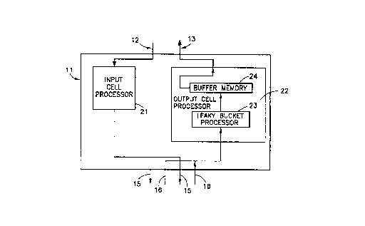
Figure 2 shows the structure of a slot controller 11 in more
detail. In accord with the preferred embodiment of the
invention, the slot controller 11 comprises an input cell
processor 21, whose structure will not be described further since
it has no bearing on the present invention. The input cell
processor 21 is connected to the input link 12 and to the input
connections 15 to the switch fabric. Cells output from the
switch fabric on connections 16 are processed for the
transmission on the output link 13 by an output cell processor 22
which includes a leaky bucket processing means 23 and a buffer
memory 24. It is noted that in Figure 2, for the sake of
clarity, only those components which relate to traffic shaping
functions are illustrated. It will be appreciated, however, that
the output cell processor 22 handles additional functions such as
CA 0221~722 1997-09-17
W 096/34469 PCTrUS~5'C560'
the writing to the cell headers of the new VPI/VCI information,
and output to the output link 13.
As previously mentioned, the output cell processor 22
comprises a leaky bucket processing means 23 and a buffer memory
24. The leaky bucket processing means 23 receives cells arriving
from the switch fabric and determines for each cell, as
hereinafter described with reference to Figure 4, whether the
peak and sustained cell flow rates appropriate to the cell's VC
have been exceeded. If the cell conforms with the peak and
sustained flow rates specified, the cell is entered into a buffer
memory 24 at an address corresponding to the current time. If one
or the other of the peak and sustained rates has been exceeded,
so that the leaky bucket overflows, the amount of the overflow,
or of the greater of the overflows if both buckets overflow, is
added to the current time as the address for the cell in the
buffer memory 24. Thus, the onward transmission of the cell is
delayed by the amount of the overflow, to ensure that the cell
will conform with the specified rates. The cells are output from
the buffer memory 24 in order of stored time slot; i.e., the
cells are not transmitted onwards before the relevant time slot
becomes due.
Figure 3 shows a first arrangement of the buffer memory 24
forming part of the traffic shaping means in the slot controller
illustrated in Figure 2. In the arrangement of Figure 3, the
buffer memory 24 comprises a multi-~'m~nsional FIFO 31
dynamically configured in Random Access Memory (RAM). For
convenience of illustration, only a very small portion of the
buffer is shown in Figure 3. The horizontal direction in the
buffer represents different time slots arranged sequentially, the
buffer being such that the current time pointer moves along the
buffer until it reaches one end, and is then reset to the other
end so that the buffer is effectively "circular". At each time
slot, one or more ATM cells may be stored. The time slot may be
empty if no cells are assigned the same onward transmission time.
If more than one cell is assigned the same onward transmission
-
CA 0221~722 1997-09-17
W O 96134469 PCTnUS96/OS606
time, the time slot is treated as a FIFO memory, with the cells
being written to the slot sequentially and read out of the time
slot in the same order in which they are written to the slot. An
output logic means 32 is arranged to step a current time pointer
along the bu*fer according to the actual current time, but to
control output of cells according to an output time pointer which
lags behind the current time by up to approximately eight time
slots (the a]gorithm attempts to maintain a m~X;mllm of eight time
slots lag, but if many cells are present a grater lag can
sometimes develop). Conveniently, the time slots are each of
640ns duration, being thirty-two clock periods of the system
clock. In a convenient mode of operation, the output pointer
waits until the current clock has advanced by eight slots
relative to the output time, and then during the next time
interval looks at each of the eight time slots to output the
cells found. Thus, for the example shown in Figure 3, the time
slot b has three cells awaiting transmissionj and these are
transmitted in turn. The next slot, c might for example have no
cells waiting, so the output time pointer jumps to the next slot
d and causes the two cells waiting there to be transmitted in
turn. If all the waiting cells in the eight slots have not been
transmitted in the next time interval of 640ns, the output time
pointer continues to advance at eight-times the clock speed until
it "catches up" and cells are being transmitted within the
appropriate time interval. In practice, it is expected that the
set of eight slots will allow the output to keep pace with the
current time, but it will be appreciated that different numbers
of slots, with appropriate speeds, may be selected if desired or
if necessary.
Figure 4 illustrates an alternative arrangement for the
~ buffer part of the traffic shaping means, in which the cells are
stored in a series of FIFOs 41 defined dynamically in RAM, each
- VC having its own FIF0, and a buffer memory 42 stores at
appropriate time slot addresses the address of the relevant FIFO
41. Leaky bucket processing logic 43 is used to process incoming
cells in the manner hereinbefore described with reference to
CA 022l~722 l997-09-l7
W O 96/34469 PCTrUS~lC'60C
Figure 2, and as further described hereinafter with reference to
Figure 5. In a manner analogous to that described with reference
to Figure 3, the buffer memory 42 is controlled by logic 44 to
store in sequential time slots the addresses of the cells in the
FIFOs 41 instead of the actual cells, and to output the addresses
in sequence to cause the cells to be output from the FIFOs 41.
More than one address can be stored at any time slot, and the
addresses are then output in sequence on a "first in first out"
basis, in the same way as the actual cells are output in the
embodiment described with reference to Figure 3.
Figure 5 illustrates the algorithm used by the leaky bucket
processor. The algorithm shown uses two buckets, one for peak
flow and one for sustained flow, and each cell is process by both
buckets, the result of the bucket having the greatest overflow
being used to determine the time slot for the cell address (for
the embodiment shown in Figure 4) or (in the case of the system
illustrated in Figure 3) the time slot in the FIFO for the cell
itself. The new cell is received at 50 to start the process. At
51, the algorithm calculates the time interval between the stored
onward transmission time for the last cell on the same VC and the
current time at which the new cell arrives. Then the new level
of each bucket is determined at 52 by subtracting the calculated
time interval from the existing bucket level, and the new level
is used to calculate at 53 an overflow value by subtracting the
bucket maximum from the new level. If it is determined at 54
that the overflow is negative, at 55 the overflow is set to zero.
Regardless, the overflow values obtained from the two buckets
(peak and average) are compared and the greatest overflow is
selected at 56. At 57, the onward transmission time for the cell
is set to the current time plus the amount of the overflow. Each
bucket level is then incremented at 58 by the stored
predetermined increment, which is equivalent to one cell, and the
new bucket levels are written at 59 to the memory. The stored
time is then set to the onward transmission time at 60 for use in
the calculation for the next cell on the particular VC, and at 61
the system is ready to read the next cell on the VC.
CA 0221~722 1997-09-17
W O 96t34469 PCTrUS96/OS606
The resulting transmission time from the performance of the
algorithm is used to set the time slot in the buffer memory at
which the cell (in the case of the embodiment is described with
reference to Figure 3), or the cell FIFO address (in the case of
the embodiment described with reference to Figure 4) is stored.
The cell, or the address, then remains in the appropriate time
slot until tlle output time pointer determines that its contents
should be read and the cell output, either directly from the
buffer, or, in the case of the Figure 4 embodiment, from the
separate FIFO 41. The result of this operation is that the cells
are transmitted onward from the slot controller in a more
controlled manner, with the effects of bunching of the cells
having been removed.
There have been described and illustrated herein a traffic
shaping ATM network switch. While particular embodiments of the
invention have been described, it is noted intended that the
invention be limited thereto, as it is intended that the
invention be as broad in scope as the art will allow and that the
specification be read likewise. Thus, while particularly
preferred processor apparatus disclosed in co-owned applications
was described, it will be appreciated that other processor
apparatus could be utilized in accord with the principles of the
invention. Likewise, while processing of two leaky buckets for
peak and average flow rates was described, it will be appreciated
that the leaky bucket processor could process any number of leaky
buckets. It will therefore be appreciated by those skilled in
the art that yet other modifications could be made to the
provided invention without deviating from its spirit and scope as
so claimed.
.