Note : Les descriptions sont présentées dans la langue officielle dans laquelle elles ont été soumises.
CA 02216589 2001-02-14
Computer-Assisted Design Analysis Method
For Extracting Device And Interconnect Information
This invention relates to the field of semiconductor integrated circuit
structure analysis.
BACKGROUND Of THE INVENTION
In the intensely competitive field of microelectronics, detailed analysis of a
semiconductor integrated circuit product can provide valuable information as
to how ;~
particular technical problem was dealt with, overall strengths and weaknesses
of a design
approach, etc.. This information can be used to make decisions regarding
market positioning,
future designs and new product development. The information resulting from
analysis of the
product is typically provided through circuit extraction (reverse
engineering), functional
analysis and other technical means. At the core of this activity is the
process of design
analysis which, in this context, refers to the techniques and methodology of
deriving
complete or partial schematics, starting with essentially any type of
integrated circuit in any
process technology. For such technical information to be of strategic value it
must be
accurate and cost-effective, and it is very important that the information
should be timely.
A design analysis process typically involves skilled engineers manually
extracting
circuit information from a set of large "photomosaics" of an integrated
circuit (IC). Skilled
technicians and engineers perform the following sequential manual tasks:
( 1 ) Capture Image:
(i) a high magnification photograph is taken, using a camera, of a small
portion
of an IC which has been processed to expose a layer of interest.
(2) step (i) is repeated for all of various regions of interest of the layer
of the IC, ensuring
CA 02216589 2001-02-14
2
that sufficient overlap exists between adjacent photographs that will be used
to create
photomosaics.
(3) Create Photomosaics:
(ii) all adjacent photographs associated with the given IC layer are aligned
and
taped together.
(4) steps (1)-(3) are repeated for all layers (1)-(N) necessary to construct a
layout
database of the IC. All layers include interconnect layers. For example, four
sets of
photomosaics are required for a state-of the-art microprocessor employing four
layers
of interconnect: three layers of metal and one layer of polysilicon.
(5) Extract Circuit:
(iii) transistors, logic gates and other elements employed in the IC are
identified by
manually visually examining the polysilicon and lower metal interconnect
photomosaics.
(iv) interconnections between circuit elements of (iii) are traced and this
information is captured in the form of schematic drawings.
(v) drawings of (iv) are manually checked against the photomosaics and any
obvious errors are con-ected.
(6) Organize Schematic:
(vi) the drawings of (v) are organized into hierarchal functional/logical
blocks.
(7) Capture Schematic:
CA 02216589 2001-02-14
(vii) the drawings of (vi) are entered into a computer using computer aided
engineering (CAE) software tools for subsequent simulation and functional
analysis of the IC.
S Fully manual techniques for circuit extraction are not reliable since the
task of
extracting circuit information can be quite arduous and is prone to errors.
Surprisingly,
researchers have explored automated circuit extraction procedures instead of
computer-
assisted techniques. Because of the image processing techniques used to
extract circuit
information, the device must have excellent clarity on all the IC layers (i.e.
no residuals from
previous layers, and no stripping of the current layer). This is a heavy
burden for the
chemical etches used to prepare the samples (remove oxide, strip off IC
layers, clean the
sample, etc..
Some systems have attempted to be fully automated, but no system has been
designed
to aid the engineer in extracting the device and interconnect information. The
prior an
generally involves some sort of image processing or pattern recognition to
identify the
polygons which constitute the layout. Such systems are described in U.S.
Patent 5,086,477
issued February 4th, 1992 to Kenneth K Yu et al and U.S. Patent 5,191,213
issued March 2na
1993 to Haroon Ahmed et al. and also US Patent 5,694,481 issued December
2°d 1997 to
Lam et al.
In the system described in U.S. 5,086,477, the integrated circuit chip is
scanned by a
microscope or scanning electron microscope (SEM). The system identifies every
unique cell
and/or gate used in the integrated circuit. A unique abstract representation
is created for each
of these unique cells or gates, which are stored in a library.
However, without any operator guidance, the system cannot know where the
boundary of a cell lies. While the patent suggests the use of diffusion edges
to define cell
boundaries, it appears that the only way that this can be done is by manual
operator direction.
In the patented system, once all unique cells have been captured in a
reference library,
CA 02216589 2001-02-14
4
the system attempts to associate and match all abstract features contained in
the layout data
base to the cells in the reference library using classical template matching.
However because
of the magnitude of data contained in a layout data base for a typical modem
integrated
circuit, even after the data has been compressed, the processing time required
to reliably
extract a netlist is large. The difficulty and time required for the operator
directed process
becomes very difficult with a large number of cells or gates, since the number
of template
matching operations increases exponentially with the number of reference cells
and/or gates.
Once all reference cells in the patented system have been template matched to
the
data base, theoretically all features in the layout data base will have been
grouped and
classified and a netlist can be constructed. If all the features of the layout
data base have
been classified then a netlist can be constructed. If there are features of
the layout data base
that have not been classified, either the system must construct a new cell or
gate to be added
to the reference library and an operator is informed, or the operator is
informed by the system
and the operator performs this task. The cell to cell interconnect information
extraction,
which is required to construct a netlist, is said to be performed using
template matching,
which is very inefficient.
Due to the template matching approach that is required, the patented system
should be
limited to gate-array or very structured standard cell integrated circuit
analysis in which the
large majority of the cells are identical, since as the number of cells in the
integrated circuits
increase, the efficiency decreases. It is therefore inefficient for analysis
of modem ASICs or
custom integrated circuits, large and/or complex integrated circuits. The
patented system
would also be limited to applications where many devices from a few ASIC
manufacturers
are investigated, due to the investment and time required to develop separate
reference
libraries, e.g. related to a different set: of design rules.
U.S. Patent 5,191,213 relates to a technique for removing layers of an
integrated
circuit and for scanning each of the layers.
US Patent 5,694,481 issued December 2"d 1997 to Lam et al discloses a system
CA 02216589 2001-02-14
which performs the following steps, in the following order: a) image capture;
b) image
segmentation and polygon generation; c) registering (of polygon data); d)
vertical aligmnent;
e) schematic generation. Although an improvement over the prior art this
technique still has
its limitations, some of them being:
5
1. Segmentation and polygon generation results are degraded around the
boundaries of
each of the images, which increased the amount of operator interaction. This
could be
minimized, by decreasing the perimeter to area ratio of the size of each image
being
captured. This minimizes the problem without solving the source.
2. Registering of polygon data is not as precise as registering of images.
Although a
saving is generated in terms of computing time, operator time, especially at
the
vertical alignment phase, is increased.
3. Vertical alignment employs a potentially large search to align the
different IC layers
to each other. This search involves aligning sets of contacts and vias to each
other
from successive layers. This task could be hampered by a number of reasons:
i. If deprocessing was poor, contacts/vias would not necessarily be easily
replicated from layer-to-layer. Contacts/vias from successive layers may not
necessarily be available.
ii. The preferred embodiment of that invention used an SEM to perform image
capture. Any SEM magnification drift could not be accommodated in the
previous disclosure.
iii. The search for a match could potentially be quite time consuming since no
previous knowledge of a cross-reference point was available. Additionally,
due to the often repetitive nature of integrated circuits, there was a chance
of
aligning the layers at the wrong location. If the 'layer misalignment'
threshold
was set too low, no match may be found.
CA 02216589 2001-02-14
6
4. No facility for correcting 'beam twist' in an SEM-like system is provided.
None of the previous techniques has the structure and advantages of the method
included in the present invention.
SUMMARY OF THE INVENTION
The present invention overcomes the above shortcomings. A computer assisted
circuit extraction method is proposed which counters these problems. In this
disclosure, the
overhead involved with 'tuning' the image processing algorithms and/or pattern
recognition
algorithms is removed, since the polygons are created manually.
The present invention is thus significantly more adaptable and the efficiency
of layout
1 S extraction in respect of modem very large and complex integrated circuits
is greatly
improved.
In accordance with another object of the present invention there is provided a
method
for extracting design information from a semiconductor integrated circuit (IC)
or at least a
portion thereof comprising: (a) imaging at least a portion of one or more IC
layers to obtain
stored images of said portions of the IC; (b) using manual or automatic
registration
techniques to mosaic images; (c) using an IC layout package possessing a
feature of allowing
images to be displayed and moved and polygons to be created to allow the
recreation of the
IC layout in the form of polygons; (d ) exporting or storing of a polygon
database in a
standard IC layout format; (e) creating a table of transistor connections
(netlist); (f)
organizing circuit netlist into functional blocks of increasing complexity;
and (g) generating a
schematic diagram.
In accordance with yet another object of the present invention there is
provided a
method for extracting design information from a semiconductor integrated
circuit (IC) or at
least a portion thereof comprising: (a) imaging at least a portion of one or
more IC layers to
CA 02216589 2001-02-14
7
obtain stored images of said portions of the IC; (b) using manual or automatic
registration
techniques to mosaic images; (c) using an IC layout package possessing a
feature of allowing
images to be displayed and moved and polygons to be created to allow the
recreation of the
IC layout in the form of polygons; (d) exporting or storing of a polygon
database in a
standard IC layout format; and (e) creating a table of transistor connections
(netlist).
Further objects and advantages of the present invention will be apparent from
the
following description, wherein preferred embodiments of the invention are
clearly shown.
BRIEF DESCRIPTION OF THE DRAWINGS
A better understanding of the invention will be obtained by reading the
description of
the invention below, with reference to the following drawings, in which:
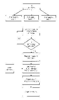
Figure 1 is a flow chart generally illustrating the present invention of
extracting
design information from a pre-existing semiconductor integrated circuit (IC).
DETAILED DESCRIPTION OF THE INVENTION
Based on the sophistication of the user and the level of automation desired, a
few
different system configurations are available - from no computer automation
beyond the
image display/manual image movement/polygon drawing/printing to a system which
performs these tasks with the added features of automated image placement and
netlist
generation. Optionally, signal tracing capabilities can be added. In all cases
the user has the
option of generating specialized symbols which are recognized by the netlist
tool as primitive
functions (i.e. transistor, inverter etc.). These are just IC layout format
cells which either a
netlist tool can recognize, or a symbol which the engineer is more familiar
with. The layout
format being generally GDSII.
To the operator, the symbols that are being placed are considered primitive.
However, below each symbol is actual layout information which can be
interpreted by
CA 02216589 2001-02-14
industry standard netlist tools (which netlist tools can be of the Verilog or
Spice or VHDL
type). The symbols may have, underneath them, a layout as simple as a single
transistor
(either n- or p- type) or even as complicated as a flip-flop, a memory array
or any other
layout entity which is repeated multiple times in a layout. The symbols have
ports on them
which the operator would use to interconnect each symbol with the other
symbols which have
been placed using the standard IC layers. The route and IC layer which the
operator uses to
interconnect each of the symbols does not necessarily need to correspond with
the
type/routing of the interconnection which is physically used in the layout,
although this may
often be the case. For example, even when extracting circuit information from
a circuit
which was fabricated using a two-layer metalization process, any number of
metalization
layers, even 6 or more, could be used to mimic the interconnections of the
symbols as long as
the netlist tool recognizes these extra layers of metalization and the
electrical connectivity of
the circuit is preserved.
It should also be mentioned that transistor sizing can be extracted from the
polygons
which are generated through the process, the true accuracy of the sizings
being dependent on
the type of imaging used.
The advantage of this method over current technologies, is that no facility
exists
which incorporates all these components. Tools are available to manipulate
pixel images
(and even include overlays), but none exist which can output data in IC
industry standard
formats. In summary, IC tools are inadequate for performing this task since
they do not have
the facility to view/manipulate pixel data and more generic image manipulation
tools are also
inadequate because they are customized for document presentation, and do not
provide the
facility to perform complicated manipulations with polygon data (i.e. extract
relative
positioning information, boolean intersections etc.).
The method flow could be as follows°
1. Image device IC layers individually. Transistor polysilicon and diffusion
areas can be
imaged together. If the device is simple (i.e. one metal, one polysilicon) -
only one
CA 02216589 2001-02-14
9
set of images may be necessary;
2. Optionally use pixel based registration techniques to mosaic the images. A
facility
must exist for an operator to manually move the pixel images. This is required
if the
operator decides to mosaic the images manually, or detects a mis-registration
produced by the automated techniques;
3. Use a package similar to an IC'. layout package which allows the drawing,
and
extraction of positions, of polygons over the images. The package must allow
the
user to toggle which set of background images should be displayed (2nd layer
metal,
1 st layer metal, etc.). Optionally, each set of background images can be
moved and
rotated with respect to a fixed point in the database. Also, optionally, basic
building
blocks such as NMOS , PMOS, NPN, PNP transistors, resistors, capacitors,
diodes,
inductors etc. can be placed instead of drawing components explicitly.
Additionally,
optional building blocks such as simple logic gates, or even complicated
structures
can be placed directly as well. These blocks can be in the form of schematic
symbols
which an engineer would be familiar with and/or physical layout symbols, which
the
computer can interpret.
4. The optional facility to either export the polygon database in a standard
IC layout
format, such as GDSII, and/or the facility to create a table of transistor
connections
netlist can be present. It should be noted that a new, more compact, netlist
may be
generated following the organizing since it can then utilize the results of
the circuit
organization;
S. The optional facility to create functional blocks of increasing complexity
in the netlist
can be available. This includes the facility to recognize standard logic
functions, or
higher-level patterns of organization.
The techniques outline above are similar to flow used to lay an IC out. The
difference, in this case, is that the operator re-creates the IC layout, using
the digital
CA 02216589 2001-02-14
representations of the physical IC as a guide. Using these techniques, even
large circuit areas
of an IC can be extracted.
It should also be noted that the step of organizing the circuit netlist into
functional
blocks of increasing complexity and the step of generating a schematic diagram
may not be
necessary when dealing with small areas.
The invention may be embodied in other specific forms without departing from
the
spirit or essential characteristics thereof. The present embodiments are
therefore to be
10 considered as illustrative and not restrictive, the scope of the invention
being indicated by the
appended claims rather than by the foregoing description, and all changes that
come within
the meaning and range of equivalency of the claims are therefore intended to
be embraced
therein.