Note : Les descriptions sont présentées dans la langue officielle dans laquelle elles ont été soumises.
CA 02216998 2004-09-30
IN-SITU DIFFUSION OF DOPANT IMPURITIES DURING
DENDRITIC WEB GROWTH OF CRYSTAL RIBBON
BACKGROUND OF THE INVENTION
This invention relates to the field of solar cells for converting
solar energy into electrical energy. More particularly, this invention relates
to
dendritic web photovoltaic cell technology.
Solar cells comprising semiconductor devices employing the
photovoltaic effect for convening solar energy into electrical energy have
long
been known. A known particular type of solar cell is made using the dendritic
crystal web growing technique in which a source material, such as silicon, is
melted in a furnace and slowly withdrawn using a seed crystal attached to a
suitable mechanical drawing apparatus along a path from the source melt
through a furnace exit port to a receiving station. Under suitable temperature
controlled conditions and a proper withdrawal rate, the melt material forms a
crystalline web having a dendritic cross-section which cools to a finished
crystalline web, This process is more fully described in"Dendritic Web Silicon
For Solar Cell Application", RG. Seidenstecker, Journal of Crystal Growth, 39
( 1977) PP. 17-22.
In order to provide the photovoltaic effect, semiconductor
junctions must be formed within the crystalline web using a suitable dopant
technique. One popular technique employed is the dopant diffusion process in
which a dopant material is diffused into the crystalline web via the two major
web surfaces to provide first and second diffusion layers of opposite
conductivity type. Diffusion has been done in the past using a gas diffusion
process in which the dopant material is in the form of a gas stream which is
permitted to flow past the web surfaces so that ions of the dopant materials
can
be diffused into the crystalline web material. This process must necessarily
be
carried out well downstream of the cxystauine web formation site, and
typically
requires a separate diffusion station, which adds complexity to the dendritic
CA 02216998 2004-09-30
2
solar cell production process. In addition, gaseous diffusion requires
separate
gas sources (for the dopant materials of opposite conductivity type) and
carefully designed and fabricated gas flow paths to prevent the dopant gas
streams from escaping to ambient or contaminating other equipment.
SUMMARY OF THE INVENTION
The invention comprises a method and apparatus for in-situ
diffusion of dopant impurities into one or both of the major web surfaces of a
growing crystalline web which avoids the disadvantages attendant upon the gas
diffusion process, which is relatively uncomplicated to implement in existing
melt furnaces and which employs solid dopant diffusion source materials to
provide the requisite concentrations of dopant materials,
From a process standpoint, the invention comprises a method of
fabricating a dendritic web photovoltaic crystal ribbon comprising the steps
o~
( 1 ) growing a dendritic crystal web including two maj or surfaces
and a dendrite from a melt source in a furnace by drawing melt material along
a
path from the melt source and permitting the melt material to cool; and
(2) directly exposing at least one of the two major surfaces of the
growing web to a substantially flat surface of a solid dopant material heated
to
a diffusion temperature as the growing web is drawn along the path, wherein
the substantially flat surface is maintained substantially parallel to the at
least
one of the two major surfaces, thereby diffusing some of said solid dopant
material into said at least one of the two major surfaces.
When the method is performed by exposing both major surfaces
of the growing web to a solid dopant material, one of the major surfaces is
exposed to a first dopant material and the other one of the major surfaces is
exposed to a second dopant
CA 02216998 1997-10-O1
3
material, the first and second dopant materials providing dopants of
opposite conductivity type.
The web is exposed by placing a solid dopant material,
preferably in planar form, in a holder adjacent a thermal source to heat
the solid dopant materiel to the diffusion temperature. The thermal
source preferably includes a solid thermal element, which is heated
alternatively by subjecting the thermal element to heat contained in the
furnace or heating the thermal element with a heating coil.
The step of exposing the web to the solid dopant material
may be performed either inside the furnace or outside the furnace.
When performed outside the furnace, the solid dopant material is
placed in thermal contact with the, thermal source adjacent the exit
port, and the thermal source preferably includes a rapid thermal heater
fixture, such as a resistance heater of conventional design.
From an apparatus standpoint, the invention comprises a
furnace having means for producing a melt source of crystal growing
material, and an exit port; means for drawing melt material along a
path from the melt source through the exit port so that a dendritic
crystal web having two major surfaces is grown as the melt material is
drawn along the path; a solid dopant material arranged along the path
in facing relation to at least one of the two major surfaces of the
dendritic crystal web; and means for heating the solid dopant material
to a diffusion temperature so that the growing dendritic crystal web is
exposed to the solid dopant material in order to create a diffusion layer
in at least one of the two major surfaces. The solid dopant material is
preferably received in a holder mounted along the path and located
either within the furnace or outside the furnace adjacent the exit port.
The means for heating the solid dopant material includes
a thermal element located along the path and at least partially
surrounding the dopant material, with the solid dopant material
arranged in thermal contact with the thermal element. An optional
CA 02216998 1997-10-O1
4
auxiliary heating coil may be arranged about the thermal element for
controlling the temperature. When the heating means is located
outside of the furnace, preferably adjacent the exit port, an auxiliary
rapid temperature external heater is provided, preferably an electrically
powered resistance heater element.
The apparatus may be arranged with single-sided or
double-sided dopant capabilities. When arranged for double-sided
dopant operation, the solid dopant material comprises a first dopant
material element arranged in facing relation to one of the first and
second major surfaces of the growing dendritic crystal web, and a
second dopant material element arranged in facing relation to the other
one of the first and second major surfaces of the dendritic crystal web
so that each of the first and second dopant material elements functions
as a diffusion source for the corresponding facing major surface of the
IS growing dendritic crystal web. The first and second dopant material
elements provide dopants of opposite conductivity types in the double-
sided configuration.
For a fuller understanding of the nature and advantages
of the invention, reference should be made to the ensuing detailed
description, taken in conjunction with the accompanying drawings.
BRIEF DESCRIPTION OF THE DRAWINGS
FIG. 1 is a sectional view of a first embodiment of the
invention;
25 FIG. 2 is a perspective view partially broken away
illustrating a portion of the Fig. 1 embodiment;
FIG. 3 is a sectional view of a second embodiment of the
invention;
FIG. 4 is a partial perspective view illustrating a portion
of the embodiment of Fig. 3;
CA 02216998 1997-10-O1
$ .
FIG. 5 is a sectional view of another embodiment of the
invention; and
FIG. 6 is a perspective view partially broken away of a
portion of the embodiment of Fig. 5.
DETAILED DESCRIPTION OF THE PREFERRED EMBODIMENTS
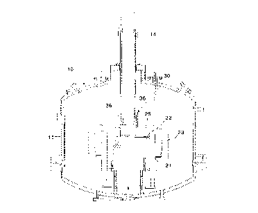
Turning now to the drawings, Figs. 1 and 2 illustrate a
first embodiment of the invention in which a vertical thermal element
and solid diffusion source and holder are positioned within a web
growing furnace. With reference to Fig. 1, a conventional furnace
generally designated with reference numeral 10 has an outer wall
structure 11 with an exit port 12. Secured to wall structure 11 adjacent
exit port 12 is a web drawing support fixture 14 for enabling a growing
web initially formed inside the furnace 10 to be withdrawn by means of
a conventional web drawing mechanism (not shown) and transferred to
a receiving station. Since the web drawing mechanism and receiving
station are well known, conventional devices, further description is
deemed unnecessary in order to avoid prolixity.
Arranged within furnace 10 is a susceptor 21 for retaining
a melt crucible (element 24 shown in Fig. 2) in which the melt material
(typically silicon) is maintained in a liquid state. An RF heater coil 23
is arranged about susceptor 21 for the purpose of heating the silicon in
the crucible in a conventional manner. Arranged above a lid portion
22 of susceptor 21 are a plurality of shields 25. Positioned centrally of
shields 25 is an in-situ diffusion fixture and solid diffusion source
generally designated with reference numeral 30.
With reference to Fig. 2, which is a perspective view
partially broken away of susceptor 21, lid 22, shields 25 and the in-situ
diffusion fixture and solid diffusion source 30, element 30 is seen to
include a vertical thermal element 31 secured in any suitable fashion to
the top surface of shields 25. Vertical thermal element 31 is preferably
CA 02216998 1997-10-O1
6
fabricated from graphite and serves as a thermal heat source for a solid
diffusion source 33 positioned in a diffusion source holder 34. Solid
diffusion source 33 is preferably a rectangular strip of diffusion source
material, such as phosphorus or boron, and may be mounted in
5 diffusion source holder 34 in any suitable fashion, such as ry forming
slots 35 along the inner facing surfaces of the end portions of holder 34.
Holder 34 is preferably formed from graphite in order to provide a
temperature stable additional heat sink for diffusion source 33. A pair
of rods 36 are secured to holder 34 in any suitable fashion, such as by
forming tapped holes extending from the upper surface inwardly of the
body of holder 34. Rods 36 extend upwardly of furnace 10 (see Fig. 1)
and exit through exit port 12 to a rod manipulating fixture (not shown)
in order to enable holder 34 and source 33 to be positioned within and
removed from vertical thermal element 31.
15 Again with reference to Fig. 2, diffusion source 33 is
arranged in facing relation with a major surface 41 of growing dendritic
web 40 which is drawn upwardly by the web withdrawing mechanism
described above. As the growing web passes through the zone of the
solid diffusion source 33, dopant ions thermally driven from diffusion
source 33 diffuse into the surface and interior of web 40. By
controlling the temperature of source 33, the withdrawal rate of web 40,
the vertical position of source 33, and the separation distance between
source 33 and web 40, diffusion impurity concentrations of desired
amounts and depths can be provided within web 40. The withdrawal
rate, separation distance between source 33 and web surface 41 and
temperature of source 33 are all typically determined empirically.
Typical temperature ranges are from about 900°C to about
1000°C.
Typical web withdrawal rates are in the range of about 1.5 cm/min.
Typical separation distances between source 33 and web surface 41 are
in the range of about 100 mils.
CA 02216998 1997-10-O1
7
While the arrangement shown for the embodiments of
Figs. 1 and 2 uses a single planar diffusion source 33 adjacent only one
major surface 41 of web 40, a second diffusion source may be
positioned within holder 34 in facing relation to the other major surface
42 of growing web 40 in order to provide simultaneous diffusion of
dopant impurities into both surfaces of growing web 40.
In the embodiment of Figs. 1 and 2, the temperature of
vertical thermal element 31, holder 34 and diffusion source 33 is
controlled by controlling the furnace temperature, and elements 31, 34
and 33 are heated by thermal conduction through shields 35 and also
the ambient temperature within the furnace. The embodiments of Figs.
3 and 4 illustrates a first alternate embodiment in which the
temperature of elements 31, 33 and 34 is also controlled by auxiliary
heating coils. With reference to Figs. 3 and 4 in which elements
common to the embodiment of Figs. 1 and 2 are designated with
identical reference numerals, a plurality of RF auxiliary heater coils 50
are arranged about vertical thermal element 31 and are used to provide
auxiliary heating for the vertical thermal element 31, holder 34 and
solid diffusion source 33. As with the embodiment of Figs. 1 and 2, the
Figs. 3 and 4 embodiment may also include a second solid diffusion
source positioned facing major surface 42 of growing web 40.
Figs. 5 and 6 illustrate still another alternate embodiment
of the invention. In this embodiment, a rapid temperature external
heater fixture 60 is mounted on a heater support column 62 outside
25 furnace 10 adjacent exit port 12 to provide auxiliary heating for the
growing web. The holder 34 and solid diffusion source 33 are both
positioned within the external heater fixture 60, which provides easier
access to these elements in order to facilitate installation and removal
of the diffusion sources 33. In addition, the embodiment of Figs. 5 and
6 eliminates vertical thermal element 31.
CA 02216998 1997-10-O1
g
Attached as Appendix A are five sheets of drawing
illustrating actual fixture details for vertical thermal element 31, source
holder 34, rods 36 and ancillary components.
As will now be apparent, the invention permits in-situ
diffusion of dopant materials into one or both major surfaces of the
growing dendritic web emerging from the melt crucible. This
arrangement eliminates the necessity for providing gaseous dopant
diffusion sources and the attendant disadvantages of such diffusion
source arrangements. In addition, the solid planar diffusion source may
be easily installed and removed from the source holder, and the relative
vertical position of the solid diffusion source 33 can be readily adjusted
by means of rods 36 to provide source temperature adjustment.
Perhaps most importantly, the invention eliminates the need for a
separate diffusion station for the dendritic web formation process,
which renders the production facility more compact and simplifies the
installation, initial set-up and process operation when producing
dendritic web photovoltaic cells.
While the above provides a full and complete disclosure
of the preferred embodiments of the invention, various modifications,
alternate constructions and equivalents may be employed, as desired.
Therefore, the above description and illustrations should not be
construed as limiting the scope of the invention, which is defined by the
appended claims.
CA 02216998 1998-04-21
APPENDIX A
500+010
.155 .000
a.010 A B C
-~n-1
4
C
~=2.~so~
x.010 A B Cm .250
3.250 ~~ .500
CA 02216998 1998-04-21
0.140 ~;000 MARKED ~F~
~~~~.010 ~~A~B~~C~~ 2.44
B
.750
°' iFi
1.755
__ __ __ I _.~.
3.50 3.062 ;
~G~
SEE DETAI L C
'- x.156 ~;000 MARKED ~G~
.010 ~ A BQ CQ
3.00
.O1 ~ A BQS
CA 02216998 1998-04-21
1.755
,_ __
__
__
6X
250
'
.
375
1
.
1
125
.
~
2X
.438
v ;
2.750
~ .010QMA DQS
DETAIL C
f--.38
1.320
1.750 _________________
_______________
___ ____
~I .12
2.500
x.010~A BQS
CA 02216998 1998-04-21
2.690
1.125 1.250
i i -A
L J
062 ~ _ .200 -
n~~~
-1.750
I~I~.010 OM A B~S CQS
z.ooo
L~I~.o~o ~M A BQS c~S
CA 02216998 1998-04-21
U
a
d"
i ~ il - li ~ i
~~r~'I'~~~~
U
U ~Q
QO . O N
O
.- O
O ~- X 'O cXD
O N N
i
O I O N
M
N O O .- I N M ai
NO O I
I
O ~ ~ 0
U
U
U
Q O
\
r 4 ~ O
~
~
~ O 0 O
0
~~
~9.-~ _
N ~ M O ~ X O
.
X ~
N ,h
CA 02216998 1998-04-21
m0
N
~Q
Z
O
O
OO
r-
O_
X
X N
M
CO
O
. ~ a
0
N
x '
N
O
M
n
o
i
tND X
N N
a
=a
o
N O~O~ X i j O
-- .-
~ O
X
N
CA 02216998 1998-04-21
N
r_
D
Q N
II 1I ~ O
II ~v
11
II O _
II
II ~ I
II
f fll V
I III I
I I11 m I ; D Q
1 III O Q I O Q
I III
U I I I I ,~ I O rQ-
Q i III 1 p
I I I I N ,- I N ~ D
I III O O
I I11 ~ I
ll~ O I I I I
N ' I 111 U a
I III 1
I I
__
:' 8 --~~
U c,Np
O
Q Y
Q
O 00
00 O
''r
N N (w 1- f O
M
r:
_ _
I ~ r I
______-__--______-__-_
I ' m I
I Q _I
PEI d' ~ O I
1 N w M r- J
I I ~ I
I 1 ~ I
_______________________ a
______________________
__ _________
I
__
U
Y
m
Q
t~ O
00 ~
t01 O
r
9
CA 02216998 1998-04-21
x.140 ~;000 MARKED ~F~
~! ~ X5.010 ~ A BQS CQS 0
2.44
.750 II
~F~
1.817
__ __ __
3.50 3.062 ' ~ I
0 I I
I
' __ __ '_,
SEE DETAI L D
~- x.156 ~;000 MARKED ~G~
~QS.OiO ~ A BQS CQS
3.00
.01 ~ A B S~
CA 02216998 1998-04-21
--i 'x'38
1.224
__________ ____
1.750 =-_-__--___---__ --_
_____
_____________ ________
____________________ _______
-_ 125
1.750 -
~ .010 ~ A BSS
i.eo
1.312
2X .657
2X .438 -' I ~- 10X .062
-- 2.000 ---
~.010~A DQS
DETAIL D
CA 02216998 1998-04-21
20.00 ---
--~ .25 +.03
.000
r0.157 ~04.OOMM~ STK
.138-40UNF-2B
3
-OB
f---- 2.~so --~
I 1 I ~ 2X .065
.410
2X .345 ~~~ ~2X .125
2X .138-40UNF-2B z .50 J 1.750
~~5.010~A B~C
.010 ~ A B C
2.031
x.010~A B~C~
2.179
.480
2X 1.000
1.125
NOTES:
SUGGESTED SUPPLIER: GOODFELLOW CORPORATION, P.O. BOX 937
MALVERN, PA 19355.
+.o~
~.23 ,00
SCALE: 2/1 4
0.250 r J~~ REMOVE
STK .500 -I
STK
LENGTH
_ r-.as+.o,
ao
SCALE: 2/1 5 --w
0.250 r J~~ REMOVE
STK .500 -I
STK
LENGTH
CA 02216998 1998-04-21
' 40~:88b MARKED ~F~
X5.010~AB~C~
~a~ r
-~ .01 ~ A B
2.760
~ .010 ~ A Bm
4.00
2X 1.
-A-
L~'IS~.010 ~~A~B~ C~
x.156~:88b MARKED ~G~
CA 02216998 1998-04-21
x.140 ~;000 MARKED ~F~
~ QS.010 Q A BQ CQ
2.44 -
.750
0.2190
rb iFi
1.125
-;~ ,
3.50 3.062 I 119
G' ~ / SEE DETAIL B
~- x.156 ~;000 MARKED 'G~
~ x.010 QM A BQS CQS
3.00
.01 ~ A 9QS
CA 02216998 1998-04-21
f--.38
2.25
.01 ~ A CAS
0.1250
0
1.750
x.010~A DQS
1 .
.062
.062
DETAIL B
x.010~~A DDS
CA 02216998 1998-04-21
m
N
Z Q
O
O
d'
I O_
M O
X
N
I
Q
I
u~
N
X
N
X
N
N
cn
07
n
N
N
'- N
O
O
a7 O N
O Z Q
H
N N I~ O
~ X
~- ~ '~ O
O
X
N