Note : Les descriptions sont présentées dans la langue officielle dans laquelle elles ont été soumises.
CA 02217146 1997-10-01
Covered Wire Connection Method and Structure
BACRGROUND OF THE lNV~ ON
This invention relates to a connection method and
structure for connecting covered wires with each other or
connecting a covered wire to another member.
As a conventional connection structure for this kind
of covered wires, an art proposed by this inventor (see
Japanese Laid-Open Patent Application No. 7-320842) will
be described.
For connecting two covered wires the outer periphery
of which is coated with a cover portion made of resin, at
their intermediate connection portions, a pair of resin
chips which are of resin material, a horn for producing
ultrasonic vibration, and an anvil for supporting the
covered wires and resin chips at the time of connection
are utilized. The anvil includes a base stand and a
support portion projecting from the base stand. The
support portion is designed in a substantially
cylindrical shape. The support portion has a bore portion
which is opened at the opposite side to the base stand
side. Two pairs of grooves are formed on the peripheral
wall of the support portion so as to cross with each
other substantially at the center of the bore portion.
The four grooves are formed so as to open on the same
side as the bore portion, extending along the projection
direction of the support portion and intercommunicate
with one another through the bore portion.
The pair of resin chips are designed in a disc shape
having a slightly smaller outer diameter than the
diameter of the bore portion of the anvil. Furthermore,
an end face of a head portion of the horn is designed in
CA 02217146 1997-10-01
a disc shape having an outer diameter which is
substantially equal to or slightly smaller than that of
the resin chips.
The respective resin chips have solder as soldering
material. The solder 15 is embedded substantially in the
center of the bottom/top surface such that a circular top
face thereof is flush with the bottom/top surface
(melting surface) of the upper and lower resin chips.
In order to connect the two covered wires to each
other, both of the covered wires are overlapped with each
other at the connection portion thereof and the
overlapped connection portions are pinched through a
solder by the pair of resin chips from the upper and
lower sides of the connection portions. Specifically,
one of the resin chips (the resin chip at the lower side)
is inserted into the bore portion of the anvil such that
the melting surface thereof is directed upward. Then, one
covered wire is inserted into the pair of confronting
grooves from the upper side of the inserted resin chip.
Then, the other covered wire is inserted into the other
pair of the confronting grooves. Finally, the other
(upper side) resin chip is inserted such that the melting
surface is directed downward. The covered wires are
arranged in the bore portion so that the respective
connection portions thereof cross each other at the
center of the bore portion. Through this arrangement,
the connection portions of the covered wires are pinched
substantially at the center of the melting surfaces of
the upper and lower resin chips respectively in the
overlapping direction.
Subsequently, the cover portions at the connection
portions of the covered wires are melted so as to be
dispersed by ultrasonic vibration. Furthermore, the
conductive wire portions (core) of the covered wires are
conductively contacted with each other at the connection
portion by pressing the covered wires from the outside of
the resin chips. Thereafter, the pair of the resin chips
CA 02217146 1997-10-01
are mutually melt-fixed at the melting surfaces to seal
the connection portion.
Specifically, the head portion of the horn is
inserted into the bore portion from the upper side bore
portion from the upper side of the finally-inserted upper
(other) resin chip and placed on the upper resin chip to
excite and press the connection portions of the covered
wires from the outside of the upper and lower resin chips
between the horn and the anvil. The cover portions are
first melted and the conductive wire portions of the
covered wires are exposed at the connection portion
between the resin chips. At this time, the melted cover
portions are extruded from the center side of the resin
chips toward the outside thereof because the connection
portions are pressed from the upper and lower sides, so
that the conductive wire portions are more excellently
exposed and surely conductively contacted with each other.
Like the press direction, the direction of the excitation
of the connection portions is set to be coincident with
the overlapping direction of the covered wires, so that
the action of extruding the melted cover portions from
the center side of the resin chips to the outside thereof
is promoted.
When the pressing and exciting operation on the
connection portions is further continued after the
melting of the cover portions, the resin chips are melted
and the confronting melting surfaces of the resin chips
are melt-fixed to each other. In addition, the outer
peripheral surface portions of the cover portions which
are adjacent to the conductively contacted conductive
wire portions and the resin chips are melt-fixed. With
this operation, the outer peripheral portions of the
conductively-contacted conductive wire portions are kept
to be coated with the resin chips.
The solder provided in the resin chips is melted by
heat generated when the resin chips are melted.
Consequently the conductive wire portions of the
CA 02217146 1997-10-01
conductively contacted covered wires are soldered at the
connection portions in the resin chips. As a result, a
higher electric performance can be obtained at the
connection portions thereby further stabilizing the
conductive characteristic.
However, in this connection structure, solder must
be melted accurately at the same timing in a series
connecting process as when the cover portion is melted
such that the conductive wire portion is exposed and
contacted with each other. Thus, the solder needs to be
buried inside of the resin chips without being exposed
from melting surfaces of resin chips respectively. When
burying the solder inside of the resin chips, in
production process of the resin chips, a special
16 treatment for sealing opening portions for the burying
with resin material is needed after the solder is buried
in the resin chips. Thus, increase in cost of the resin
chips cannot be avoided.
Further, to melt solder accurately at the above
timing, detailed setting and management of a position of
the solder in the resin chips and ultrasonic melting
condition (particularly temperature) must be conducted.
Thus, conductive connecting procedure becomes complicated
and such an intrinsic effect of this technology that
conductive connection is performed by a simple method may
be lost.
Further, the solder needs to contain a mixture of
chemical active substance (flux) for improving leaking
characteristic for core wires composing the conductive
wire portion. In this technology which solders the
connection portions and simultaneously seals it, this
kind of flux needs to be contained in the resin chips.
Thus, there is a fear that the connection portions may
corrode due to flux so that conversely reliability
relating to electrical connecting performance may be
reduced.
CA 02217146 1997-10-01
SU ~ ARY OF THE lNVl~;N-~L ION
Accordingly, an object of the present invention is
to provide a covered wire connection method and
connection structure in which covered wires can be
conductively connected with each other at cheap price and
easily and a connection state with excellent electric
characteristic can be obtained stably.
In order to achieve the above object, according to
the present invention, there is provided a covered wire
connection method and structure comprising steps of and
formed by steps of overlapping two covered wires each of
which comprises a conductive wire portion composed of
plurality of core wires and a covered portion covering an
outer periphery of the conductive wire portion, pinching
an overlapping portion of the covered wires between a
pair of resin chips, pressurizing and exciting the
overlapping portion pinched by the resin chips using an
ultrasonic vibration welding apparatus so as to melt and
disperse the cover portion, thereby to expose the
conductive wire portion and electrically conductively
connect the conductively wire portions of the covered
wires at the overlapping portion and so as to melt-fix
the pair of resin chips to seal the connected overlapping
portion of the covered wires with the melted resin chips,
wherein a crossing angle at the overlapping portion of
the two covered wires is set to not less than 45~ to not
greater than 135~.
According to the construction described above, the
covered wires are overlapped with each other at the
connection portions (overlapping portion) and the
overlapped connection portions are pinched by a pair of
the resin chips. Then, the cover portions are melted and
dispersed by ultrasonic excitation and further pressed
from outside of the resin chips. With such a relatively
simple method, the covered wires can be conductively
contacted with each other with the connection portions in
sealing condition.
CA 02217146 1997-10-01
After the covered wires are conductively contacted
with each other at the connection portions, the pair of
the resin chips are melt-fixed to each other so as to
seal the connection portions. With melted and hardened
resin chips, a high mechanical strength can be obtained
at the connection portions.
The crossing angle of the covered wires is set to
not less than 45~ to not greater than 135~ in which a
pressure applied from the resin chips acts on the covered
wires substantially equally without losing balance so
that the core wires are excellently loosened and the
loosened core wires are gradually spread to flat shape.
Thus, the conductive wire portions of both the covered
wires are in contact with each other at plural positions,
so that connecting state having excellent electric
characteristic and with low contact resistance can be
obtained. That is, the crossing angle of the covered
wires is set to not less than 45~ to not greater than
135~ in which a pressure applied from resin chips acts on
covered wires substantially equally without losing
balance so that the core wires are excellently loosened
and the loosened core wires are gradually spread to flat
shape. Thus, the conductive wire portions of both the
covered wires are in contact with each other at plural
positions. Thus, no special treatment is needed to the
resin chips and a connecting state having excellent
electric characteristic can be obtained stably at cheap
price.
At least one of the resin chips may contain wire
supporting portions for restricting the crossing angle of
the two covered wires at the overlapping portion at a
desired angle.
According to the construction described above, it is
possible to set the crossing angle at a desired angle
easily by means of the wire supporting portions provided
in the resin chips without providing other member such as
the anvil with a means for restricting the crossing angle.
CA 02217146 1997-10-01
At least one of the resin chips may be made of a
transparent material.
According to the construction described above, the
spreading of the core wires on the connection portions
can be visually checked. Thus, simplification of quality
inspection can be achieved.
A covered wire connection structure may more
comprises a protective case for covering the overlapping
portion of the two wires as well as neighboring portions
thereof. The protective case may contain a case body and
lid body, one side of the case body may be open, the lid
body may be to close an opening portion of the case body,
the resin chips may be formed in the case body and the
lid body such that they are integral therewith
respectively, and at least one of the case body and the
lid body may contain protruding portions for restricting
the crossing angle of the two wires at the overlapping
portion at a desired angle.
According to the construction described above, the
pair of the resin chips are melt-fixed to each other to
seal the connection portions with their conductive
connecting state and at the same time, the case body is
connected with the lid body. Thus, the connection
portions and the neighboring portions are covered with
protective cases. That is, by melt-fixing the pair of
the resin chips to each other, the connection portions of
two covered wires are sealed and at the same time, the
case body is connected with the lid body in the
protective case. Thus, for the connection of the case
body with the lid body, other process is not required and
increase of the number of processes is not induced
despite an increase of parts. Further by the protective
case, protection of the connection portions and the
neighboring portions can be achieved.
Further, the two covered wires ca be maintained at a
desired crossing angle because they are caught at the
time of ultrasonic excitation. Thus, after the sealing,
CA 02217146 1997-10-01
the connection portions are kept to be conductively
contacted with each other while crossing at the desired
crossing angle. Thus, a stabilized electrical
performance can be exerted.
The protruding portions may be formed so as to have
both side walls, the two covered wires may be in contact
with and curved by the walls so as to cross each other at
the desired crossing angle, and the protruding potions
may be arranged so as to oppose each other adjacent to
the resin chips.
According to the construction described above, the
connection portions of the two covered wires are arranged
so as to cross each other at the desired angle on the
resin chip between the protruding portions disposed so as
to oppose each other. Because the protruding portions
are disposed adjacent to the resin chips, the width of
the protruding portion (width between both the side
walls) necessary for obtaining a desired crossing angle
can be set to a small value so that the protruding
portions can be designed in compact fashion. Further, a
distance between the opposing protruding portions is
reduced, so that the crossing state of the connection
portions can be maintained stably.
At least one of the case body and the lid body may
contain wire introducing portions for introducing the two
covered wires from the protective case in parallel.
According to the construction described above, the
two covered wires in which the connection portions are
crossed at the desired crossing angle can be introduced
in parallel through the wire introducing portions from
the protective case. Thus, it is possible to provide
such a covered wire connection structure which can be
realized preferably as a wire harness.
The case body and the lid body may be formed
integrally with each other through a hinge portion.
According to the construction described above, by
turning the lid body through the hinge portion, the lid
CA 02217146 1997-10-01
body can be set to the opening portion of the case body
easily. Further, by this setting, the pair of the resin
chips formed on the case body and the lid body each are
arranged such that their melting surfaces oppose each
other. That is, because the case body and the lid body
are molded integrally through the hinge portion,
management of parts is facilitated. Further, by only
turning the lid body through the hinge portion, the lid
body can be set to the opening portion of the case body.
Thus, positioning of respective parts is not necessary
thus simplifying assembly work.
BRIEF DESCRIPTION OF THE DRAWINGS
Fig. 1 is a perspective view showing a covered wire
16 connection structure according to a first embodiment,
Fig. 2 is an enlarged plan view of the connection
portion of Fig. 1,
Fig. 3A shows side sectional views schematically
showing states of resin chips currently being pressed and
excited just after the connection; and shows a state
magnified about nine times,
Fig. 3B shows side sectional views schematically
showing states of resin chips currently being pressed and
excited just after the connection; and shows a state
magnified about thirty times,
Fig. 4A shows side sectional views schematically
showing a state during connection of the resin chips
being pressed and excited; and shows a state magnified
about nine times,
Fig. 4B shows side sectional views schematically
showing a state during connection of the resin chips
being pressed and excited; and shows a state magnified
about thirty times,
Fig. 5A shows side sectional views schematically
showing a state after connection of the resin chips
pressed and excited; and shows a state magnified about
nine times,
CA 02217146 1997-10-01
Fig. 5B shows side sectional views schematically
showing a state after connection of the resin chips
pressed and excited; and shows a state magnified about
thirty times,
Fig. 6A shows side sectional views schematically
showing a state just after connection of the resin chips
for reference; and shows a state magnified about nine
times,
Fig. 6B shows side sectional views schematically
showing a state just after connection of the resin chips
for reference; and shows a state magnified about thirty
times,
Fig. 7 is a side sectional view showing
schematically a state after connection of the resin chips
for reference magnified by about thirty times;
Fig. 8 is a diagram showing a relation between
crossing angle and contact resistance;
Fig. 9 is a perspective view showing a connecting
structure of the covered wires according to a second
embodiment;
Fig. 10 is a sectional view taken along the lines X-
X in Fig. 9;
Fig. llA is a perspective view of a free state of a
protective case for use in a third embodiment;
Fig. llB is a perspective view of an appearance of
major parts after two covered wires are connected
according to the third embodiment; and
Fig. 12 is a plan view showing the conductive
connecting state of the core wires of two covered wires
according to a third embodiment.
DESCRIPTION OF THE PREFERRED EMBODIMENTS
Hereinafter, a first embodiment of the present
invention will be described with reference to the
accompanying drawings.
Fig. 1 is a perspective view showing a covered wire
connection structure according to the instant embodiment.
CA 02217146 1997-10-01
Fig. 2 is an enlarged plan view of the connection portion
of Fig. 1. Figs. 3-5 are side sectional views showing
schematically a state of a resin chip currently under
pressing and excitation. Figs. 3A and 3B show a state
just after the connection is started, Fig. 4A and 4B show
a state during connection and Figs. 5A and 5B show a
state after the connection is completed. Fig. 5A of the
respective Figures indicates a state enlarged about nine
times and Fig. 5B thereof indicates a state enlarged
about thirty times. Figs. 6A, 6B and 7 are side
sectional views showing schematically a state of resin
chip for reference. Figs. 6A and 6B show a state just
after the connection is started and Fig. 7 indicates a
state after the connection is completed. Fig. 6A
indicates a state enlarged about nine times and Fig. 6B
indicates a state enlarged about thirty times. Fig. 8 is
a diagram showing a relation between crossing angle and
contacting resistance.
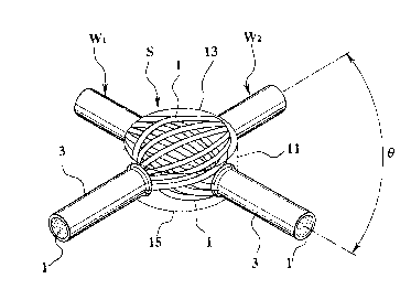
According to the instant embodiment shown in Fig. 1,
two covered wires W1, W2 each of which comprises a
conductive wire portion 1 and a cover portion 3 which is
formed of resin and coated around the outer periphery of
the conductive wire portion, are conductively connected
to each other at connection portions (overlapping
portion) S thereof as shown in Fig. 1. The respective
conductive wire portions 1 of the covered wires Wl, W2
are each composed of seven core wires (see Fig. 2).
In order to connect two covered wires Wl, W2, a pair
of resin chips 13, 15 which are resin materials 11, a
horn for producing ultrasonic vibration (not shown) and
an anvil (not shown) for supporting the covered wires Wl,
W2 and the resin chips 13, 15 at the time of the
connection are utilized. The anvil has a bore portion
which is open upward and has a circular cross section and
two pairs of groove portions which confront each other
with respect to substantially the center of the bore
portion for containing the covered wires W1, W2. These
CA 02217146 1997-10-01
four groove portions are open on the same side as the
bore portion and the mutually facing groove portions
intercommunicates with each other through the bore
portion. A crossing angle of lines connecting the
mutually facing groove portions is the crossing angle~in
which the covered wires W1, W2 are conductively connected
with each other. That angle is set to not less than 45~
to not greater than 135~ (90~ in the instant embodiment).
Meanwhile, because the structures of the horn and the
anvil are substantially the same as conventional, a
detailed description thereof is omitted.
The pair of the resin chips 13, 15 are formed in a
circular shape having a slightly smaller than the bore of
the anvil and contains no soldering material unlike
conventional case. The resin chips 13, 15 are made of
acrylic resin, ABS (acrylonitrile-butadiene-styrene
copolymer) resin, PC (polycarbonate) resin, PVC
(polyvinyl chloride) resin, PE (polyethylene) resin, PEI
(polyetherimide), PBT (polybuthylene terephtalate) or the
like. Generally, the material is harder than vinyl
chloride for use in the cover portion 3. With respect to
the suitability of these resin for use as the resin chips
13, 15, the applicability can be recognized in all the
resins in term of the conductivity and conductivity
stability and if judging from appearance and insulation
performance as well, particularly PEI resins and PBT
resins are suitable.
The respective resin chips 13, 15 have melting
surfaces 13a, 15a (see Figs. 3-5) which are contacted
with each other when the resin chips 13, 15 are
overlapped with each other vertically in the bore portion
of the anvil and the connection portions S in which two
covered wires W1, W2 cross each other are located in the
center of the melting surfaces 13a, 15a.
In order to connect the two covered wires Wl, W2,
first the covered wires W1, W2 are overlapped with each
other at the connection portions S and the overlapped
CA 02217146 1997-10-01
connection portions S are pinched vertically by a pair of
the resin chips 13, 15. Concretely, one resin chip 15 is
inserted into the bore portion of the anvil so that its
melting surface 15a is directed upward and one covered
wire Wl is inserted into confronting groove portions of
one pair such that it is located over the resin chip 15.
Then, the other covered wire W2 is inserted into the
other confronting groove portion. Finally, the other
(upper) resin chip 13 is inserted with its melting
surface 13a directed downward. Both the covered wires W1,
W2 are arranged such that the respective connection
portions S cross each other in the center of the bore
portion. Consequently, the connection portions S are
pinched in the center of the melting surfaces 13a, 15a of
the upper and lower resin chips 13, 15 vertically in the
overlapping direction. With this condition, the crossing
angle~between the cored wires Wl and W2 is limited to
substantially 90~ which is a crossing angle of the
confronting groove portions.
Subsequently, the cover portions 3 at the connection
portions S of the covered wires are melted so as to be
dispersed by ultrasonic vibration. Furthermore, the
conductive wire portions (core) of the covered wires Wl,
W2 are conductively contacted with each other at the
connection portion S by pressing the covered wires from
the outside of the resin chips 13, 15. Thereafter, the
pair of the resin chips 13, 15 are mutually melted at the
melting surfaces 13a, 15a to seal the connection portion
S (see Figs. 3-5).
Specifically, the horn is inserted onto the upper
side (other side) of the finally-inserted upper resin
chip 13 and the connection portions S are excited and
pressed from the outside of the upper and lower resin
chips 13, 15 between the horn and the anvil. The press
of the connection portion S is performed by pressing the
horn toward the anvil, and the press direction is
coincident with the overlapping direction of the covered
CA 02217146 1997-10-01
wires.
When the resin materials 11 are melt-fixed to each
other by the ultrasonic vibration, the excitation is
preferably performed in a direction which substantially
perpendicularly intersects to the connection surface of
the resin materials 11 because it provides the most
excellent melt-fixing state. Therefore, the direction of
the excitation of the connection portion S is set to a
direction which crosses the confronting surfaces 13a, 15a
of the resin chips 13, 15, that is, it is set to be
coincident with the overlapping direction of the covered
wires W1, W2. With this arrangement, longitudinal
vibration is produced from the horn.
When the connection portions S are pressed and
excited in the above state, the cover portions 3 are
first melted and the conductive wire portions 1 of the
covered wires W1, W2 are exposed at the connection
portion S between the resin chips 13 and 15. At this
time, the melted cover portions 3 are extruded from the
center side of the resin chips 13, 15 toward the outside
thereof because the connection portions S are pressed
from the upper and lower sides, so that the conductive
wire portions 1 are more excellently exposed and surely
conductively contacted with each other. Like the press
direction, the direction of the excitation of the
connection portions S is set to be coincident with the
overlapping direction of the covered wires W1, W2, so
that the action of extruding the melted cover portions 3
from the center side of the resin chips 13, 14 to the
outside thereof is promoted.
If the pressing and excitation of the connection
portions S are continued after the cover portions 3 are
melted, the resin chips 13, 15 are melted such that the
melting surfaces 13a, 15a of both the resin chips 13, 15
are melt-fixed to each other. Outer peripheral faces of
the cover portions 3 adjacent to the conductive wire
portions 1 which are conductively contacted with each
14
CA 02217146 1997-10-01
other are melt-fixed to the resin chips 13, 15.
Consequently, the outer peripheral faces of the
conductive wire portions 1 conductively contacted are
covered with the melted resin chips 13, 15 (see Fig. 1).
Because the crossing angle~between the covered
wires W1 and W2 is set to 90~, a force from the resin
chips 13, 15 is applied to the covered wires Wl, W2 (core
wires of the conductive wire portion 1) substantially
equally with keeping a balance when the connection
portions S are pressed and excited. As a result, first
the core wires are loosened and the loosened core wires
are spread gradually so that they become flat (see Figs.
3-5). Consequently, the conductive wire portions 1 of
both the covered wires W1, W2 are contacted with each
other at plural positions (see Fig. 2).
Here, an example of results of the experiments will
be shown. If the crossing angle~is 90~, it has been
recognized that the number of contact points between both
the core wires exceeds 30 points. This indicates that
they are contacted with each other at very many points
because the m~;mum number of contact points is 49 (see
Fig. 2) if seven core wires are made to contact other
seven core wires.
Further, if a percentage of occurrence of unbalanced
spreading of the core wires is obtained when the crossing
angle~is changed in a range between 90~ and 30~, it is
0% in a range between 90~ and 60~ and it is as low as 11%
when the crossing angle is 45~. However, it is
recognized that the percentage is as high as 89~ when the
crossing angle is 30~. If the crossing angle~is small
(about 30~), as shown in Figs. 6, 7, the core wires of
the upper covered wire W2 enter in between the core wires
of the lower covered wire W1 easily so that a force
applied from the resin chips 13, 15 acts with lost
balance. On the other hand, if the crossing angle~is
large (90~), as shown in Figs. 3-5, the core wires of the
upper covered wires W2 are unlikely to enter in between
CA 02217146 1997-10-01
the core wires of the lower covered wires W1. This is
because a force applied from the resin chips 13, 15 act
equally with keeping balance.
If a relationship between the crossing angle ~ and
contact resistance is obtained through experiments, as
shown in Fig. 8, the contact resistance is less than 5mQ,
when the crossing angle ~ is 90~ -45~ . If the crossing
angle becomes smaller than 45~, the contact resistance
rises largely and when 30~, the contact resistance
10 exceeds 5mQ.
From what has been said above, it is found that if
the crossing angle ~ is decreased from 90~, the condition
of spreading of the core wires is deteriorated so that
the number of contact points between the core wires is
15 reduced and then contact resistance increases. A range
of the crossing angle ~ in which stable conductive
contacting can be obtained with a low contact resistance
is preferably 90~ i45~ (45~ - 134~). Particularly 90~ is
the most appropriate.
According to the connection method of the instant
embodiment, by pressing the resin chips 13, 15 from
outside so as to melt and disperse the cover portion 3
with the covered wires W1, W2 overlapped at the
connection portions S and the connection portions S
25 pinched by a pair of the resin chips 13, 15, the covered
wires W1, W2 can be conductively connected with each
other at the connection portions S. Thus, when
conductively connecting the covered wires W1, W2, it is
not necessary to remove the cover portion 3 and obtain
30 conductive connection by a simple operation.
Further, according to the connection method and the
connection structure obtained thereby, after the covered
wires W1, W2 are conductively connected with each other
at the connection portions S, the upper and lower resin
35 chips 13, 15 are melt-fixed to each other to seal the
connection portions S. Thus, by the melted and hardened
resin chips 13, 15, a high mechanical strength can be
CA 02217146 1997-10-01
obtained at the connection portions S.
Further, because the resin chips 13, 15 have only to
have a dimension capable of pinching the connection
portions S to be conductively contacted from up and down,
6 area necessary for the connection can be restricted to a
small area. Further, because the connection portions S
are sealed by the resin chips 13, 15, it is possible to
ensure a sufficient insulation.
Thus, by such a high mechanical strength and a
sufficient insulation, conductive characteristic between
the covered wires Wl and W2 at the connection portions S
can be stabilized.
Furthermore, the covered wires W1, W2 are pinched by
the pair of the resin chips 13, 15 in the overlapping
direction thereof and the connection portions S are
pressed and excited between the horn and the anvil from
the outside of the resin chips 13, 15 and the direction
of the pressing is set to the same as the direction in
which the covered wires Wl,W2 are overlapped with each
other. Thus, when the connection portion S is pressed,
the melted cover portions 3 are extruded out from the
center portion of the resin chips 13, 15 toward outside
so that the conductive wire portions 1 are exposed
excellently thereby obtaining a secure conductive
contacting state. Further, because the direction of
excitation to the connection portion S is set to the same
as the direction in which the covered wires W1, W2 are
overlapped with each other like the pressing direction,
it is possible to obtain excellent melting condition of
the resin chips 13, 15 and enhance an action of pushing
out the cover portions 3.
Further, the crossing angle~between the covered
wires W1 and W2 is set to be not less than 45~ to not
greater than 135~ in which a pressure applied from the
resin chips 13, 15 acts substantially equally on the core
wires without losing balance so that they are excellently
loosened, the conductive wire portions 1 of the covered
CA 02217146 1997-10-01
wires Wl, W2 are contacted with each other at plural
positions. Consequently, a stable connecting state with
an excellent electric characteristic can be obtained.
Particularly, in the instant embodiment, the crossing
6 angle~is set to 90~ in which the core wires can be
loosened most excellently. Thus, it is possible to
achieve improvement of electric characteristic and
stabilization thereof.
Further, it is not necessary to make special
treatment for the pair of the resin chips 13, 15 such as
embedding of solder unlike conventional case. Thus, they
can be structured in a cheap construction. Further,
different from a case in which solder is provided, no
flux is produced at the connection portions S, so that
reliability of electric connection performance is not
reduced.
Further, by making at least one of the resin chips
13, 15 with a transparent material, it is possible to
visually check the spreading of the core wires on the
connection portions S. Thus, the conductive connecting
state between the covered wires Wl and W2 can be visually
recognized thereby simplifying quality inspection.
It is permissible to use the resin chips 13, 15
having a relatively low viscosity at the time of melting.
Then, when melting the resin chips 13, 15 so as to
surround the connection portion S, the melted resin chips
13, 15 may be filled in gaps between plural core wires
composing the conductive wire portion 1 in the
neighboring conductive wire portions 1 excluding the
connection portion S to fill gaps formed between the
cover portions of the covered wires Wl,W2 and the core
wires or gaps formed between the core wires with resin
material 11 thereby obtaining an effect of sealing
against water inside of the covered wires Wl, W2. Thus,
for example, in a case in which one end of the covered
wires Wl, W2 is connected to a portion requiring
waterproof (waterproofed portion) and the other end
CA 02217146 1997-10-01
thereof is connected to a portion not requiring water
proof (non-waterproofed portion), water or the like
enters inside of the covered wires W1, W2 from the other
end due to capillary phenomenon and flows inside of the
covered wires W1, W2. However, water is prevented from
entering to the one end by the aforementioned effect of
sealing against water. Thus, it is possible to secure
water proof performance at the one end without providing
the other end with water proof structure. That is, if
both ends of the covered wires Wl,W2 are connected to the
water proofed portion and the non-waterproofed portion,
it is possible to secure waterproof performance in the
waterproofed portion without providing the non-
waterproofed portion with a waterproofing structure, by a
simple and cheap method and structure.
Next, a second embodiment of the present invention
will be described with reference to the accompanying
drawings.
Fig. 9 is a perspective view showing a covered wire
connection structure according to the instant embodiment.
Fig. 10 is a sectional view taken along the lines X-X.
The same components as the aforementioned first
embodiment are provided with the same reference numerals
and a description thereof is omitted.
According to the instant embodiment, the lower resin
chip 45 is provided with wire containing grooves 53 which
are wire supporting members for restricting the crossing
angle~at the connection portions S between the two
covered wires W1 and W2 to a desired angle.
The lower resin chip 45 comprises a chip body 47
which is of substantially cylindrical shape and in which
a top surface thereof is a melting surface 47a, a
circumferential portion 51 formed around the chip body 47
in a doughnut shape and a groove portion 49 formed
between the chip body 47 and the circumferential portion
51 which is open upward and in a donut configuration.
The circumferential portion 51 has two pairs of wire
CA 02217146 1997-10-01
containing grooves 53 (four positions) which confront
with each other with respect to the center of the melting
surface 47a and are open upward. The crossing angle of a
line connecting the mutually facing wire containing
grooves 53 is the crossing angle~used when conductively
connecting the covered wires Wl and W2. That angle is
set to be not less than 45~ to not greater than 135~ (90~
in the instant embodiment) like the first embodiment.
The melting surface 47a of the chip body 47 is formed at
a position (height) deviated upward or downward from a
bottom of the wire containing groove 53. If the covered
wires Wl, W2 are set in the mutually confronting wire
containing grooves 53 and pressed, the covered wires W1,
W2 are bent at peripheral portions of the chip body 47
and the groove portion 49 and then contained in the wire
containing grooves 53 such that they are temporarily held.
Both the covered wires Wl, W2 cross each other at a
desired crossing angle~substantially in the center of
the lower melting surface 47a. Meanwhile, the upper
resin chip 43 is formed in a circular shape so that a
bottom face thereof is a melting surface 43a like the
first embodiment. The upper and lower melting surfaces
43a, 47a are of substantially the same shape and
dimension. Although according to the instant embodiment,
26 only the lower resin chip 45 is provided with the wire
containing grooves 53, it is possible to provide both the
upper and lower resin chips 43, 45 with such wire
containing grooves 53 or provide only the upper resin
chip 43 with the wire containing grooves.
According to the instant embodiment, in addition to
the effects of the first embodiment, it is possible to
set the crossing angle~at any desired angle by means of
the wire containing grooves 53 provided in the lower
resin chip 45 without providing additional groove
portions for restricting the crossing angle~in the anvil
like the first embodiment.
Further like the first embodiment, by making at
CA 02217146 1997-10-01
least one of the resin chips 43, 45 with a transparent
material, it is possible to visually check the conductive
connecting state between the covered wires W1 and W2 to
some extent, and it is possible to ensure waterproofing
effect within the covered wires W1, W2 by filling gaps
between neighboring core wires excluding the connection
portions S with melted resin chips 43, 45 when the resin
chips 43, 45 are melt-fixed to each other with the
connection portions S set therebetween.
Next, a third embodiment of the present invention
will be described with reference to the accompanying
drawings.
Fig. llA is a perspective view of a free state of a
protective case for use in the instant embodiment. Fig.
llB is a perspective view of an appearance of major parts
after two covered wires are connected according to the
instant embodiment. Fig. 12 is a plan view showing a
conductive contacting state of the core wires of two
covered wires according to the instant embodiment.
The instant embodiment of the present invention is
constructed mainly of a pair of the resin chips 13, 15
and a protective case 60 having a protruding portion 64
for restricting the crossing angle of two covered wires
W1, W2 to a desired angle.
The protective case 60 comprises a case body 61 in
which a wire containing portion 61a for two covered wires
W1, W2 is formed so as to open to one side and a lid body
62 formed in a plate shape having a thick portion 62a for
closing an opening portion of the wire containing portion
61a.
Of the pair of the resin chips 13, 15, one resin
chip 13 is formed so as to protrude substantially in the
center of an inside surface (side located inside of the
case 60 when closed) of a thick portion 62a of the lid
body 62 integrally with the lid body 62. The other resin
chip 15 is formed so as to protrude substantially in the
center of a bottom of the wire containing portion 61
CA 02217146 1997-10-01
integrally with the wire containing portion 61. The
resin chips 13, 15 have melting surfaces 13a, 15a
respectively which are protruded therefrom. The resin
chips 13, 15 are constructed so that the respective
melting surfaces 13a, 15a face each other when the lid
body 62 is closed.
The protruding portions 64 are formed in the wire
containing portion 61a of the case body 61 in one pair.
That is, the pair of the protruding portions 64, 64 are
formed to have both side walls 64a, 64a with which two
covered wires W1, W2 are in contact so as to be bent at a
desired crossing angle, and allocated adjacent to the
resin chip 15 so as to oppose each other. At this
protruding portion 64, the crossing angle may be
controlled by a distance between the side walls 64a and
64a, that is, a width of the protruding portion 64. This
protruding portion 64 is formed with such a width to
obtain a desired crossing angle. At this time, the
protruding portion 64 is protruded over the melting
surface 15a of the resin chip 15 and lower than a depth
of the wire containing portion 61. Both the side walls
64a, 64a of this protruding portion have the
aforementioned function.
Preferably as in the instant embodiment, wire
introducing portions 65 for introducing two covered wires
W1, W2 from the protective case 60 in parallel are formed.
The wire introducing portions 65 are formed by cutting in
a U-shaped groove form both ends of the wire containing
portion 61a in which the pair of the protruding portions
64, 64 are located, such that they are opened in the same
direction as that of the wire containing portion 61a and
go through those ends. Two wire introducing portions 65
are provided on each of both the ends of the wire
containing portion 61a. Corresponding to the wire
introducing portions 65, square pillar pressing portions
66 which enter into the wire introducing portions 65 for
pressing the covered wire Wl(W2) when the lid body 62 is
CA 02217146 1997-10-01
closed are formed on both sides of the thick portion 62a
of the lid body 62.
Preferably as in the instant embodiment, the case
body 61 and the lid body 62 are formed integrally with a
hinge portion 63.
In the instant embodiment having the above
protective case 60, a covered wire connection structure
is obtained in the following manner.
First, as shown in Fig. 11, two covered wires W1, W2
are set in the case body 61. That is, the respective
covered wires W1, W2 are placed such that their
connection portions S cross each other substantially in
the center of the melting surface 15a of the resin chip
15 and both sides of the connection portion S are curved
along both the side walls 64a of the protruding portions
64 and engaged in the corresponding wire introducing
portions 65. The respective connection portions S of two
covered wires W1 and W2 are caught by the pair of the
protruding portions 64, 64 such that they intersect each
other at a desired crossing angle.
Next, the lid body 62 is turned via the hinge
portion 63 and the pressing portions 66 are engaged into
the wire introducing portions 65. Then, the wire
containing portion 6la of the case body 61 is closed with
the lid body 62. In this closing state, the connection
portions S are pinched by the melting surfaces 13a, 15a
of the resin chips 13, 15 in the center thereof
vertically in a direction of overlapping the resin chips
13, 15.
The same covered wire connection structure as in the
first embodiment can be obtained by ultrasonic excitation
using the horn as in the first embodiment. According to
this connection structure, as shown in Fig. llB, the two
covered wires W1, W2 are introduced in parallel from both
ends of the protective case 60 in such a state in which
both sections of the covered wires adjacent to the
connection portions S are pressed by the pressing
CA 02217146 1997-10-01
portions 66 and engaged in the wire introducing portions
65.
According to the instant embodiment, in addition to
the effects of the first embodiment, the following
particular effects may be exerted.
That is, the pair of the resin chips 13, 15 are
melt-fixed to each other such that the connection
portions S are sealed in a state in which they are
conductively connected and the case body 61 is connected
with the lid body. Consequently, the connection portions
S and the neighboring portions are covered with the
protective case 60 and protected against any external
force.
Further, the two covered wires W1, W2 are fixed at
the protruding portions 64 by ultrasonic excitation such
that they are maintained at a desired crossing angle.
After sealing, the connection portion S is in conductive
connecting state so that the core wires 1 cross each
other at a crossing angle~(substantially 90~ in the
instant embodiment) thereby exerting a stabilized
electric performance.
Because the protruding portions 64 are disposed
adjacent to the resin chips 15, a width of the protruding
portion 64 necessary for obtaining a desired crossing
angle at the connection portion S may be designed to be
small. Consequently, it is possible to design the
protective case 60 in a compact size. Further, a
distance between the opposing protruding portions 64 and
64 is reduced such that the connection portion S located
therebetween can be maintained stably at a desired
crossing angle.
Further, according to the instant embodiment, as
shown in Fig. llB, the two covered wires W1, W2 in which
the connection portions S are intersected at a desired
crossing angle are introduced in parallel through the
wire introducing portions from the protective case 60.
Thus, this may be preferably applicable as wire harness.
24
CA 02217146 1997-10-01
Further, according to the instant embodiment, the
case body 61 and the lid body 62 are formed integrally
with each other through the hinge portion 63. Thus,
management of the parts is facilitated and only by
turning the lid body 62 via the hinge portion 63, it can
be set to the open portion of the case body 61. Thus,
positioning of the parts is not necessary and the
assembly work may be simplified.
As a modification of the instant embodiment, the
following may be considered.
If at least one of the resin chips 13, 15 is made
with a transparent material and then a case 61 (or lid
body 62) in which that resin chip 15 (or 13) is disposed
is also made with a transparent material, the conductive
connecting state of the two covered wires W1, W2 can be
visually checked thereby simplifying quality inspection.
Further, the protruding portions 64 and the wire
introducing portions 65 may be provided on the lid body
62. Further, the hinge portion 63 may be cut off after
the lid body 62 is connected to the case body 61.