Note : Les descriptions sont présentées dans la langue officielle dans laquelle elles ont été soumises.
CA ~ 2 2 1 7 7 6 6 1 9 9 7 ~ 8
Micl. -ch~n;cal rate-of-rotation sensor
The invention relates to a micromechanical rate-
of-rotation sensor based on the Coriolis principle and
having two plate-like o~cillators to be stimulated
electrostatically to oscillate in antiphase.
The measurement of rates of rotation by determin-
ing Corioli~ ~orces i~ known, and i8 used in more than
one sensor o~ this generic type.
In the coriolis rate-of-rotation sensors which
are currently available on the market, use i made o~
piezoelectric effects for the st;m~ tion~ for example,
of oscillations and for reading out; cf., only by way o~
example, EP O 563 761 Al, EP O 563 762 Al,
EP O 520 467 A1, EP O 520 468 A2, EP O 533 163 A2,
EP O 460 089 B1, GB 2 251 072 A, CA 1 313 065 A,
EP O 298 511 B1, EP O 318 972 Bl, EP O 638 783 A1 and
US 5 247 252 A.
Since the piezoelectric materials used for the
said purposes in microengineering have temperature-
dependent material parameters which are very different in
comparison with silicon, the re~ult is high temperature
dep~n~ncies and non-reproducibilities of the zero point
of such rate-of-rotation sensors, which severely restrict
their field of application.
Rate-of-rotation sensors with micro~?ch~n;cal
elements can already be obtained. On the other hand,
purely micromech~n;cal solutions for a compact ~ensor are
not as yet on the market. Howeverr micromechanical
solutions in which corioli~ accelerations are measured
are known from patent publications; cf. US 5 101 702 A,
CH 682 844 A5, GB 2 251 688 A, DE 40 22 495 A1,
EP O 574 143 Al, EP O 634 629 A1, US 5 203 208 A,
EP O 442 280 A2, US 4 750 364 A, EP O 623 807 A,
EP O 620 415 Al, GB 2 276 241 A, US 4 884 446 A and
DE 40 41 582 A1.
For oscillating structures in a micromechanical
design in Si technology, capacitive actuators are sug-
gested for the stimulation and, re~pectively, capacitive
CA 02217766 1997-10-08
bridge circuits for reading out; cf. GB 92 009 30,
EP 0 586 437 A1, US 5 207 685 A, DE 40 41 582 A1.
For the capacitive drive of an oscillating micro-
mechanical structure, the most effective force direction
i8 the vertical one between two opposed, oppositely
polarized plates. For this reason it is expedient, for
~uch an oscillating structure, to select an arrangement
in which two oppositely polarized plates 100 and 200,
respectively, can be used for driving the oscillator 101
(cf. Fig. 4). The schematic signal diagrams underneath
the sectional illustration of the o~cillator clarify the
passes of the excitation signals which are applied to the
upper plate 100 (electrode 1) and, respectively, the
lower plate 200 (electrode 2).
If very small distances are used between the two
drive capacitor surfaces between the upper plate 100 and
the oscillator 101, on the one hand, and between the
lower plate 200 and the oscillator 101 on the other hand,
then adequately high driving forces may be achieved using
comparatively small voltages (e.g. 5 V).
Xowever, the disadvantage of this arrangement,
known in principle, according to Fig. 4 (cf., for
example, US 4 884 446) is that the small distances
between the drive capacitor surfaces simultaneously
restrict the m~;mllm oscillator amplitude of the oscil-
lator 101 to a fraction o$ just these capacitor plate
spacings, and for small oscillator attenuations very high
requirements must be placed on the gas atmosphere within
which the oscillator arrangement is located.
Under the influence of the coriolis acceleration,
an amplitude that is orthogonal to the oscillator move-
ment is generated, and can be used for measuring the rate
of rotation. In the example of Fig. 4, the rate of
rotation that is drawn in generates coriolis forces which
point out of the plane of the figure. However, this
arrangement has the further disadvantage that the
reaction forces of the oscillator movement are introduced
into the environment of the sensor, and can bring about
interference with the measured values.
CA 02217766 1997-10-08
.
In order to avoid this last-mentioned
disadvantage, double oscillator arrangements have been
proposed, as is shown by Fig. 5 (cf. also
GB 2 251 688 A). The first oscillator 50 and the second
oscillator 60 move in antiphase. A rate of rotation whose
vector is perpendicular to the drawing plane produces
torques about this common axi~ of rotation 55 at the
frequency of the oscillator movements. Using this known
arrangement, it is possible to achieve large oscillator
amplitudes. However, this arrangement has the disadvan-
tage that, given capacitive drive via differential
capacitors, the driving forces act between surfaces which
are located perpendicular to the plane of the wafer and
which can be produced with small distances exactly
parallel to one another only with difficulty. Non-uniform
air gaps at the oscillators 50, 60 then have an effect as
a stimulus about the axis of rotation and influence the
zero point of the sensor considerably. This effect is
temperature-dependent. A further di6advantage of this
arrangement with capacitive stimulation consists in the
relatively small driving forces, attempts being made,
according to more recent proposals, to reduce these by
means of comb-like electrodes.
The invention is based on the object of providing
a micromechanical rate-of-rotation sensor according to
the coriolis principle in which interference with
measured values as a result of reaction forces on account
of oscillator ",o~G~.cnts do not occur and in which, in
spite of the desired small distances between drive
capacitor surfaces, in principle no or significantly
fewer restrictions with respect to a permissible
oscillator amplitude have to be taken into account, and
which can be produced cost-effectively using
micromechanical engineering.
The solution according to the invention, in the
case of a micromechanical rate-of-rotation sensor based
on the coriolis principle and having two plate-like
oscillators to be stimulated electrostatically to oscil-
late in antiphase, consists in the fact that the oscil-
CA 02217766 1997-10-08
lators can be produced fro~ single-crystal wafers using
micromechanical engineering, and are arranged one above
another in two planes, like layers, perpendicular to the
plane of the wafer, and the direction of oscillation is
located perpendicular to the plane of the plates. This
allows cost-effective production using micromechanical
processes, such as etching and wafer bon~;ng.
According to the invention, the oscillators are
connected at one side or at two opposite sides in each
case to a part o~ a plate-like support structure, via
which the electrostatic stimulation of oscillation is
performed perpendicular to the plane o~ the wafer, the
inherent ~re~uency of the support structure preferably
being selected to be higher than that of the oscillators.
Fur~h~rmQre, the support ~tructure parts are configured
such that their reaction forces mutually cancel each
other.
In order to permit (~till) greater oscillation
amplitudes perpendicular to the plane of the wafer for
the oscillators, the thickness of the oRcillatorg rnnn;n~
between the two parts of the support structure is
di~tinctly lower than that o~ the ~upport structure
serving for the stimulation of oscillation. On the other
hand, the thickness of the support structure is selected
such that the smallest possible drive capacitor gaps
result for the electrostatic stimulation of oscillation
in the region of the support structure.
The oscillators are preferably connected in one
piece to the parts of the support structure, via in each
case at least one articulation strut of low thickness.
This one-piece oscillator/support combination is, then,
for its part held on one side or two sides by in each
case a spring strut in a frame surro~n~;ng the arrange-
ment of oscillator and support structure, the spring
strut preferably being configured as a leaf spring
element or as an oblique spring element which essentially
permits only rotational ~.~ve~.ents of the oscillator and
suppresses linear deflection movements of the oscillator.
An advantageous implementation of such a micro-
CA 02217766 1997-10-08
mechanical rate-of-rotation sensor consist~ in the
oscillators, together with the part~ connected thereto in
one piece via the articulation ~truts of the support
structure and of the frame, being formed, preferably by
means of anisotropic etching, from two layers of a wafer,
which layers, for the purpose of mutual insulation, are
oxidized on the respectively mutually facing surface and
are connected to one another by silicon fusion bo~;ng to
form a double oscillator structure. The double oscillator
structures, arranged one above another in alignment, are
sealed off hermetically at the upper and lower side by
nonconductive cover plates that are bonded to the frameQ.
The oscillator structures are then located in the housing
which iB thus formed, in a vacuum or in an inert gas
atmosphere under low preQQure.
The invention and further advantageous details
are explained in more detail below with reference to the
drawings in an exemplary ~hodiment. In the drawings:
Fig. 1 shows the sectional representation of a double
oscillator structure of a rate-of-rotation sensor
according to the coriolis principle with features
according to the invention;
Fig. 2 shows in an exploded representation the layer
construction of the double oscillator structure
according to Fig. 1, produced from a total of
four wafer planes supplemented by an upper and a
lower side cover plate;
Fig. 3 shows the basic sectional representation of a
cover plate to clarify ~k; ng through-contact
with electrodes applied to its inner surface~:
Fig. 4 shows a known plate oscillator structure, already
explained;
Fig. 5 shows a known double oscillator structure, like-
wise already explained, having oscillators
arranged alongside each other in one plane;
Fig. 6 shows the perspective partial view of a double
oscillator structure having features according to
the invention, which is articulated at one side;
Fig. 7 shows a double oscillator structure correspon~;ng
-
CA 02217766 1997-10-08
to Fig. 6, including a surro--n~;ng frame
arrangement, but without upper and lower cover
plates;
Fig. 8 shows a double oscillator structure CorreBpOn~; ng
to Fig. 6 with one-sided articulation via articu-
lation struts located in a [111] plane, which
overall form a type of crossed-spring
articulation; and
Fig. 9 shows the double oscillator structure of Fig. 8
within a surrol-n~ g ~rame arrangement, once more
without upper and lower covering plates.
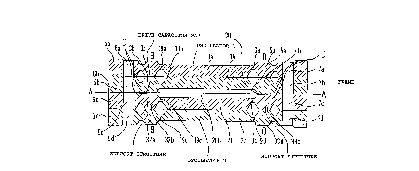
Fig. 1 shows firstly, in a sectional representa-
tion, the basic construction and the arrangement of a
two-layer oscillator structure for a micromechanical
~ate-o~-rotation senso~ m~ing use of coriolis forces to
obtain a rate-of-rotation signal.
In contrast to the known construction according
to Fig. 5 (cf. also GB 2 251 688 A) having two masses
that are located alongside each other and oscillate in
opposition, in the case of the exemplary embodiment
according to the invention and according to Fig. 1, the
oppo~itely oscillatins structures are not loc~ted along-
side one another in a plane but above one another in
various planes, specifically such that the reaction
forces of the oscillator dynamics mutually cancel each
other completely.
In the example illustrated, the o~cillator
arrangement has two oscillator elements la, lb and 2a,
2b, respectively, each having two layers, which are in
each case connected at both sides via articulation struts
9a, l9a and 9b, l9b and - in relation to the lower
oscillator 2a, 2b via articulation ~truts 9c, l9c and 9d,
l9d - in one piece to plate-like support parts 4a, 3a and
4b, 3b, on one side, and 33c, 33d and 32a, 32b on the
other side. The support parts 3a, 3b and 4a, 4b and,
respectively, 32b, 32a and 33c, 33d are for their part
connected via spring struts 5, that is to say 5a, 5b, 5c
and 5d and, respectively, 7, that is to say 7a, 7b, 7c
and 7d, to a surrounding ~rame 6, that is to say 6a, 6b,
CA 02217766 1997-10-08
6c, 6d, likewise in one piece. The individual layers thus
comprise, for example in relation to the uppermost layer
in Fig. 1, in one piece the frame 6a, connected via the
spring strut 5a to the support part 3a, that is connected
via the articulation strut l9a to the oscillator element
la, which merges at the right side via the articulation
strut 9a into the right side support part 4a, which in
turn is connected via the spring ~trut 7a to the right
side part of the frame 6a. An oscillator structure of
this type is produced ~rom a wafer material, for example
by means of an anisotropic etching process. Between the
individual layers of the two-layer double oscillator
structure, the wafer plates are oxidized, that is to say
mutually electrically insulated, and then connected to
each other by Si ~usion bon~; ng,
As Fig. 1 readily reveals, the distance between
the upper oscillator la, lb and the lower oscillator 2a,
2b is comparatively large, with the result that large
oscillation amplitudes are al~o possible. On the other
hand, a drive capacitor gap 30 between the left side
support parts 3a, 3b and 32b, 32a on one side and the
right side support parts 4a, 4b and 33c, 33d is
relatively small, as desired, 80 that good stimulation of
oscillation is possible using comparatively low levels of
a pulse voltage. As mentioned above, the inherent fre-
quency of the support structure parts 3a, 3b and 4a, 4b
and, respectively, 32b, 32a and 33c, 33d, which are
thicker in comparison with the oscillator elements, i8
selected to be different from, in particular higher than,
the inherent frequency of the two oscillators la, lb and
2a, 2b.
The spring struts 5a to 5d and 7a to 7d,
respectively serving for the suspension or holding of the
two double oscillator structures in the frame 6 having
the frame parts 6a to 6d are - as can be seen better from
Fig. 2 - configured as leaf spring elements, which are
compliant for rotational movements about the y axis (A-A)
and largely suppress linear movements in the ~z and -z
direction.
CA 02217766 1997-10-08
As can be seen, in contrast to the known double
oscillator arrangement according to Fig. 5, the double
oscillator according to Fig. 1 and Fig. 2 is not stimu-
lated directly but rather via the support structure 3a,
3b and 4a, 4b and, respectively, 32b, 32a and 33c, 33d.
This support structure has a greater rigidity than the
oscillators la, lb and 2a, 2b and causes only small
movements at the resonant frequency of the oscillators,
but cnmmlln;cates this stimulus to the oscillatorR which,
as illustrated, have a large distance or clearance 200 in
order to build up a relatively large oscillator
amplitude. Since the oscillators la, lb and 2a, 2b are
not driven directly, this clearance 200 can in principle
be configured to be arbitrarily large, which allows good
stability to be achieved for the oscillator~ at a high
quality number. On the other hand, the capacitor gap 30
for the stimulation can be ~elected in the sub-micrometre
range, as a result of which adequately large driving
forces may be achieved even at Rmall voltages. Given
sufficiently low attenuation and ~uitable ~timulation
phase, the oscillator amplitude is summed over the drive
amplitudes to ~orm o~cillator amplitudes which may lie
orders of magnitude higher. The greater distance of the
oscillators 1 and 2 from one another and from the sur-
ro~n~;ng components makes the abovementioned high oscil-
lation quality pos~ible.
A special feature of the construction illustrated
can also be seen in the fact that the driving forces are
not ~upported on a base structure from which they have to
be transmitted to the oppositely moving halves of the
support structure 3, 4 and 32, 33 respectively. Rather,
the driving forces are effective exclu~ively directly
between the two respective halves of the support
structure.
Since the two double-layer oscillators 1, 2 move
in opposition, in the case of this arrangement no
reaction forceR are emitted to the outside. Conversely,
transverse disturbances from the outside are effective in
the opposite sense on the two oscillators, a~ a result of
CA 02217766 1997-10-08
the opposed o~cillator movements, so that the influences
of said disturbances mutually cancel each other in the
output signal.
In the case o~ rotational movements o~ the entire
sensor about the axis A-A, the two oscillators 1, 2 are
moved in opposition out of their oscillation plane. The
result i~ to produce a torque, synchronous with the
oscillator movement, about the axis A-A, which torque is
also absorbed by the Qupport structure. Since the support
structure 3, 4, together with the oscillators 1, 2, is
fastened in a frame, rotational mo~ements in the region
B of the Qupport structure can be read out capacitively.
In this case it is possible for the left half of the
support structure 3a, 3b and 32a, 32b on the one side,
and the right half of the support Qtructure 4a, 4b and
33c, 33d on the other side to be read out separately. In
this manner, therefore, it is possible either for effects
of rotations about the axiQ orthogonal to the Gentre of
the figure to be compensated for in the signal and/or to
be measured in a second channel.
In the example illustrated, the oscillators and
the upport structure are held by the abovementioned
parallel spring struts 5, 7 and 5', 7', configured as
leaf springs, in order to increase the rotational stiff-
ness about the axis orthogonal to the drawing plane.These leaf spring elements permit rotational movements of
the oscillators about the y axis. If the parts la and lb
and 2a and 2b of the two double oscillator structures are
mutually insulated as mentioned above by means of oxide
layers, then the potentials for the stimulation and for
the reading out are electrically isolated, resulting in
considerable advantages for the control of speed, as well
as for the coupling in and design of the restoring
electronics and the driving electronics.
Since the support structure in the regions B (cf.
Fig. 1) executes only very small movements, this result~
in the further advantage that, by means of the small
drive capacitor gaps 30, great sensitivity can be
achieved for reading out rotational movement~.
CA 02217766 1997-10-08
-- 10 -
The electrodes needed for reading out the
oscillator movements, that i8 to say the exciter oscilla-
tion~, and the electrode~ needed for reading out the
rotational movements in the region of the support
structure (rate-of-rotation induced) may be applied as a
metal coating on the respective inner side of the
baseplate and cover plate 26 and 27 sealing the oscil-
lator ~tructure.
In order to achieve the necessary low attenuation
of the two oscillators, a negative pressure that is
~table over the service life of the sensor mu~t be
maintained in the oscillator environment. The necessary
tightness of the housing can be achieved by the
anodically bonded baseplate or cover plate 26 and 27 made
of a nonconductive material, for example of glass. The
electrode connections are contacted through via apertures
in the ba~eplate or cover plate and sealed off in a
gastight manner by likewise bonded Si islands, which will
now be explained in more detail below with reference to
Fig. 2.
This Fig. 2 shows the drawn-apart exploded
illustration of a complete micromechanical rate-of-
rotation sensor of a type of construction according to
the invention. The four central layer-like oscillator
structures have already been explained by reference to
Fig. 1. The upper oscillator 1 comprise~ the two parts la
and lb, which are oxidized for the purposes of insulation
on the mutual contact surfaces and are firmly connected
by Si fusion bonding (SFB). The oscillator 2 with its
parts 2a and 2b is of similar construction. The oscil-
lators 1 and 2 are stimulated to o~cillate in antiphase.
In order to set a desired compliance, the thick-
ness of the articulation struts 9a, 9b and l9a, l9b,
respectively and 9c, 9d and l9c, l9d, respectively, which
form a trench-like depression, may be ~elected
appropriately.
The re~; ng out of the transverse oscillator
movements in the direction +z or -z is carried out via
capacitor surface~ 12 and 13, constructed as metal
CA 02217766 1997-10-08
coatings, which are applied on the inner side to the two
bondable insulating plates, that i8 to say the cover
plate 27 and the baseplate 26, and are connected via
apertures in these insulation layers to bonded silicon
5 islands 20, 21 and 28, 31. The through connection can be
produced, just like the electrodes themselves, in the
sAme operation by applying a conductive layer. Fig. 2
also reveals, in a schematic block circuit representa-
tion, the connection o~ the ~aid connections to speed
control electronics or from resetting electronics.
In the same way - in the example illustrated in
Fig. 2, shown only for the baseplate 26 - surface-like
electrodes 8, 9 and 10, 11 for re~; ng out the rotational
movements induced by rates of rotation, which are trans-
mitted ~rom the oscillators 1 and 2 to the support
structure parts 3a, 3b and 32a, 32b, respectively and 4a,
4b and 33c, 33d, respectively, are constructed. Each one
of these electrodes is connected via a metallic conductor
track 34, 35, 36, 37, 38 and 39 to a cone-like or conical
leadthrough 14, 15, 16, 17, 18, which is also metallized.
Fig. 3 shows an exemplary embodiment for thi~ type of
through contacting. The conical apertures are sealed off
to the outside by in each case an anodically bonded on,
conductive silicon island, which hermetically seal o$f
the senAor above and below. These conductive silicon
islands at the same time form or are provided with
contact platelets 20, 21, 22, 23, 24 and 25. The
baseplate 26 and the cover plate 27 are bonded anodically
onto the frames 6, 6'. Identical cover plates may be
u~ed. Electrical contact may be made with the Aaid
electrode layers via the silicon islands or the contact
platelets 20 to 25.
Fig. 2 also reveals, in a schematic design, how
the two double oscillators are to be connected electri-
cally and to be stimulated. For example, the upper partoscillator la can be connected via the frame to a con-
stant potential +UCO~Jt The capacitor 1eA~;ng to earth
indicates the A.C. screening. The second part oscillator
lb then has applied to it exciter pulses +U~c from drive
CA 022l7766 l997-l0-08
- 12 -
electronics. The upper part 2b of the second double
oscillator can, as illustrated, be at fixed potential,
for example earth, or else have applied to it appropriate
negative pul~es -U~xc by the drive electronics.
In the exemplary embodiment illustrated, the
read-out electrode for the oscillator movement has been
divided into the electrodes 8 and 9 (or lO and 11), as a
result of which there is the possibility of designing the
capacitive read-out symmetrically and of suppressing
irradiations to a large extent.
Fig. 6 illustrates a first exemplary emboA;m~nt
of a double oscillator structure which, in principle, is
constructed in exactly the same way as that explained
above using Fig. l, but with the difference that the
oscillators 1 and 2, which are likewise two layers in
each case, are stimulated only via a single narrow
capacitor drive gap 30, and for each oscillator element
la, lb and 2a, 2b in each case only one articulation
strut 90a to 90d and in each case only one support part
4a, 4d and 33c, 33d is provided. Furth~rmore, there is
provided for each oscillator element 1 and 2 in each case
one spring ~trut 70 and 70', arranged centrally on the
front side, via which the respective electrical
connection can also be made. In the inter~;ate planes,
that i8 to say in relation to the inner oscillator
elements lb and 2a, spring struts 71 to 74, arranged
offset with respect to the centrally arranged spring
elements 70, 70', are provided. As a result of this
offset arrangement of the spring struts 70, 70' and 71 to
74, a considerable increase in the rigidity in the
respective plane (wafer plane) of the oscillator elements
la, lb and 2a, 2b is achieved.
Fig. 7 illustrates the configuration, modified
with respect to the embodiments first described, of the
frame structure 6, 6~. Integrally moulded on the centre
of the long side are mutually aligning mounting attach-
ments 60, while side contacts 40, 41, 42 and 43, arranged
offset in relation to one another, are constructed on one
or both narrow sides of the frames.
CA 02217766 1997-10-08
The embodiment according to Fig. 8 of a double-
layer oscillator structure differs from that according to
Fig. 6 by a different type of construction of spring
struts 80 to 83 and 80~ to 83', which are obli~ue on one
side, align with one another and mutually cross. While
the actual plate-like oscillator structure, articulated
on one side, ~rom the ~ree (le~t side) end as far as the
front, articulation side front face consists of
individual ~100] Si wafers, the spring struts 80 to 83
and 80' to 83' are formed by anisotropic etching in the
forward direction, that i8 to say from ~111] planes, to
be specific, as Fig. 8 readily reveals, in the m~nner of
a single crossed-spring articulation. As is obvious to
those skilled in the art, the design form of an oscil-
lator structure according to Fig. 8 offers some produc-
tion advantages with, at the same time, an improvement in
the rigidity in the planes of the wafers.
Finally, Fig. 9 shows the finished layer con-
struction of a micromechanical rate-of-rotation sensor
according to the invention having an oscillator struature
according to Fig. 8, but still without the cover plate~
26 and 27. The frame structure corresponds to that of
Fig, 7,
Using the invention, a rate-of-rotation sensor
that can be produced completely using micromechanical
engineering and is based on the coriolis principle is
provided, in which two oscillators are stimulated via
support structures that are configured in such a way that
symmetry in constructional terms completely avoids the
stimulation of structure resonances as a result of
external vibrations. This support ~tructure accepts from
the oscillators the tor~ues induced by rates of rotation,
the re~;ng out being performed via a very narrow air gap
which is far smaller than the transverse oscillator
amplitudes.
By contrast with previously disclosed micro-
mechanical rate-of-rotation sensors that are based on the
coriolis principle, according to the invention the
stimulation of the oscillators 1, 2 is performed perpen-
CA 02217766 1997-10-08
- 14 -
dicular to the respective plane of the wafer. The
disadvantages mentioned of capacitive horizontal stimula-
tion are avoided in this way and, becau~e of a very
narrow drive gap, comparatively large forces may be
achieved with relatively small stimulation voltageA.
Furthermore, in contrast to known rate-of-rotation
sensors of the type described here, it i~ not the move-
ments, caused by coriolis accelerations, of the
individual oscillator~ that are read out, these movement~
being superimposed on the much larger stimulation oscil-
lations. Rather, the effects of the corioli8
accelerations of the two o~cillators 1, 2 on the common
~upport ~tructure are capacitively detected. As a result,
on the support 8tructure the reaction force8 of the
individual part oscillators cancel each other completely,
at least to a large extent. The contradiction which
initially ari8e8, that the smalle8t possible gaps are
needed for the capacitive stimulation and re~ ng out
but the largest possible gaps are on the other hand
needed for the movement of the part 08cillators, is
countered, according to the invention, using the idea
that the individual part oscillators are ~eated on a
common stimulation structure. This common stimulation
structure enables small stimulation gaps 30, whilç a
larger movement gap 200 is provided for the o~cillators
1, 2.