Note : Les descriptions sont présentées dans la langue officielle dans laquelle elles ont été soumises.
CA 022l997l l997-ll-03
LINEARIZING CIRCUIT FOR CURRENT-FEEDBACK-
CONTROLLED SUPPLY OF LIGHT-EMITTING DIODES
BACKGROUND OF THE INVENTION
10 1. Field of the invention:
The present invention is concerned with a linearizing
circuit consisting of passive filtering components, such as a resistor and
a capacitor, and associated to a load, such as a set of light-emitting
diodes, having a non linear voltage/current characteristic. The function
of the linearizing circuit is to produce from the intensity of the current
supplied to the load a feedback voltage signal having an amplitude
varying linearly with the amplitude of the voltage applied to said load.
Such a feedback voltage signal can be required by a controller circuit, for
example a power factor controller in view of conducting a current-
feedback-controlled supply of the load.
2. Brief description of the prior art:
Many designs of linearizing circuits have been proposed
in the past. Most of these designs are costly and unduly complex; this is
CA 02219971 1997-11-03
the case for example of a linearizing circuit consisting of a complex
arrangement of differential amplifiers.
Increasing the manufacturing cost of a product sold at
5 relatively low price can be catasl~ophic to the marketability of the product.
This is the case of light-emitting-diode lamps used as trafffic signal light.
OBJECTS OF THE INVENTION
An object of the present invention is therefore to
overcome the drawback of the above discussed prior art by providing a
low cost linearizing circuit made of passive filtering components.
SUMMARY OF THE INVENTION
More specifically, in accordance with the present
invention, there is provided an electric system comprising (a) an electric
load having a non linear voltage/current characteristic, (b) a source for
supplying the load with a voltage, and a feedback-controlled current
having an intensity varying non linearly with the amplitude of the voltage
supplying the load, and (c) a controller circuit responsive to an input
voltage feedback signal for controlling the amplitude of the voltage
supplying the load. According to the invention, the electric system further
CA 022l997l l997-ll-03
comprises a current-to-voltage converter for converting the current
supplying the load to a current-representative voltage signal, and a
linearizing circuit consisting of passive filtering components having
respective impedance values related to the non linear voltage/current
characteristic of the load for producing, in response to the current-
representative voltage signal, the input voltage feedback signal having an
amplitude varying linearly with the amplitude of the voltage supplying the
load although the intensity of the current supplying the load varies non
linearly with the amplitude of the voltage supplying the load.
The present invention also relates to a light-emitting-
diode lamp comprising (a) a set of light-emitting diodes each having a non
linear voltage/current characteristic, (b) a source for supplying the set of
light-emitting diodes with a dc (direct currrent) voltage, and a feedback-
controlled dc current having an intensity varying non linearly with theamplitude of the dc voltage, and (c) a controller circuit responsive to an
input voltage feedback signal for controlling the amplitude of the dc
voltage. In this lamp, the improvement comprises a current-to-voltage
converter for converting the dc current supplied to the set of light-emitting
diodes to a current-representative voltage signal, and a linearizing circuit
consisting of passive filtering components having respective impedance
values related to the non linear voltage/current characteristic of the light-
emitting diodes for producing, in response to the current-representative
voltage signal, the input voltage feedback signal having an amplitude
which varies linearly with the amplitude of the dc voltage although the
intensity of the dc current varies non linearly with the amplitude of the dc
voltage.
CA 022l997l l997-ll-03
The use of passive filtering components for constructing
the linearizing circuit greatly reduces the cost associated to the
manufacture of this circuit. Low cost manufacture of the linearizing circuit
is important to reduce the price of the lamp on the market.
Preferably, the passive filtering components of the
linearizing circuit comprise a resistor having a first terminal for receiving
the current-representative voltage signal and a second terminal
connected to an input of the controller circuit, and a capacitor having a
10 first terminal connected to the second terminal of the resistor and a
second terminal connected to the ground, so that the input voltage
feedback signal is produced on the interconnected second terminal of the
resistor and first terminal of the capacitor.
In accordance with another preferred embodiment, the
current-to-voltage converter comprises a resistive component through
which the dc current flows to thereby generate the current-representative
voltage signal across the resistive component.
The objects, advantages and other features of the
present invention will become more apparent upon reading of the
following non restrictive description of preferred embodiments thereof,
given by way of example only with reference to the accompanying
drawings.
CA 022l997l l997-ll-03
BRIEF DESCRIPTION OF THE DRAWINGS
In the appended drawings:
Figure 1 is a graph showing that the voltage/current
characteristic of a light-emitting diode is sensitive to temperature; and
Figure 2 is a schematic block diagram of the electronic
10 circuit of a light-emitting-diode lamp according to the invention,
comprising a linearizing circuit formed of passive filtering components.
DETAILED DESCRIPTION OF THE PREFERRED EMBODIMENT
Although the preferred embodiment of the present
invention will be described hereinafter with reference to an application of
the linearizing circuit to a light-emitting-diode lamp, it should be
understood that this will not limit the use of the present invention to that
particular application.
A light-emitting diode requires a current-feedback-
controlled electric supply for the following reasons.
Figure 1 is a graph of the voltage/current characteristic
of a given t,vpe of light-emitting diode widely used in the fabrication of
CA 022l997l l997-ll-03
traffic signal lights. More particularly, the graph of Figure 1 shows that
the voltage/current characteristic of a light-emitting diode is sensitive to
temperature and that the current through a light-emitting diode changes
very rapidly and non linearly with the voltage across this light-emitting
diode. Figure 1 therefore demonstrates that electric supply of a light-
emitting diode cannot be voltage-feedback-controlled since the voltage
across the light-emitting diode changes with temperature and that the
current through the light-emitting diode widely changes with voltage.
For a constant voltage of 1.8 volt, Figure 1 shows that
the intensity of the current through the light-emitting diode is about 7.5
mA at a temperature of -25 ~C, 20.5 mA at a temperature of +25 ~C, and
30 mA at a temperature of +60 ~C. Voltage feedback control would
therefore be very detrimental to the lifetime of the light-emitting diode.
The intensity of the current through the light-emitting diode at a
temperature of +60 ~C is therefore, for a constant voltage of 1.8 volt,
about 1.6 time higher than the intensity of the current at a temperature of
+25 ~C.
For example, if a light-emitting diode is supplied with a
constant voltage and the intensity of the current in the light-emitting diode
is 32 mA at a temperature of +25 ~C, extrapolation of the curves of the
graph of Figure 1 indicates that the intensity of the current in the light-
emitting diode at a temperature of +60~C will be 51 mA, that is 1.6 time
higher. If 32 mA represents a current intensity 1.28 time higher than the
nominal current intensity of the light-emitting diode, a current of 51 mA is
approximately twice this nominal current intensity. Therefore, a current
CA 022l997l l997-ll-03
as high as 51 mA will be calasl,ophic for the lifetime of the diode since
the current intensity in a light-emitting diode should not overstep 1.7 time
the nominal current intensity.
It is obvious from the foregoing description that voltage
feedback control of the supply of a light-en ,itling diode is not suitable, and
that current feedback control is required to ensure durability of the light-
emitting diode.
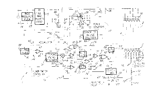
Referring to Figure 2, the LED lamp is generally
identified by the reference 1. It comprises a set 2 of light-emitting diodes
such as 3. The set 2 is formed of a plurality of subsets such as 4 of
serially interconnected light-emitting diodes 3. The subsets 4 of serially
interconnected light-emitting diodes 3 are connected in parallel to each
other to form the set 2.
A resistor 5 has a first terminal 6 connected to the
cathode 7 of the last light-emitting diode 3 of each subset 4, and a
second terminal 8 connected to a first terminal 9 of a current-to-voltage
converter 10. The current-to-voltage converter 10 has an second terminal
11 connected to the ground. As illustrated in Figure 2, the current-to-
voltage converter 10 is formed of two serially interconnected resistors 12
and 13 which produce a voltage signal having an amplitude proportional
to the intensity of current flowing through these resistors 12 and 13. Of
course, the serial resistors 12 and 13 can be replaced by a single resistor
of adequate resistance value.
CA 02219971 1997-11-03
The set 2 of light-emitting diodes 3 is supplied by an
alternating current (ac) source 14. The alternating voltage and current
from the ac source 14 is rectified by a full-wave rectifier bridge 15 and
supplied to the anode 16 of the first diode 3 of each subset 4 through a
power converter 17. A switching device (not shown) can be provided to
selectively connect the alternating current source 14 to the lamp 1 in
order to control supply of the light-emitting diodes 3.
Therefore, the current flowing into each subset 4 of light-
10 emitting diodes 3 has a value limited by the resistor 5. Also, the currentflowing in all the subsets 4 of light-emitting diodes 3 flow through the
serial resistors 12 and 13 of the current-to-voltage converter 10 to convert
the total current flowing through the set 2 of light-emitting diodes 3 into a
corresponding current-representative voltage signal delivered onto an
output 18 of the converter 10.
To allow a controller 19 to perform a current feedback
control of the supply of the set 2 of light-emitting diodes 3, a linearizing
circuit 20 is required. The controller 19 is, in the illustrated example, the
power factor controller manufactured and commercialized by the
company Motorola and identified by the reference MC34262. The
controller 19 is not capable of conducting a direct current feedback
control of non linear loads such as light-emitting diodes.
As " ,e, ltiolled in the foregoing description, many designs
of linearizing circuits have been proposed in the past. An example is a
costly, unduly complex arrangement of differential amplifiers. Since the
CA 02219971 1997-11-03
characteristics and properties of the light-emitting diodes 3 (load) are very
well known and documented, and since the costs for providing a product
such as a lamp must be kept as low as possible, the present invention
provides a low cost and very simple linearizing circuit formed of passive
5 elements.
More specifically, referring to Figure 2, the linearizing
circuit 20 is, in fact, a filter circuit formed of passive elements. In the
example of Figure 2, the linearizing circuit 20 comprises a resistor 21
10 having a first terminal 22 connected to the output 18 of the current-to-
voltage converter 10, and a second terminal 23 connected to an input 24
of the controller 19. The linearizing circuit 20 also comprises a capacitor
25 connected between terminal 23 of the resistor 21 and the ground.
The function of the linearizing circuit 20 is to transform
the non linear relation between the LED supply dc voltage at the output
26 of the power converter 17 and the dc current supplied to the set 2 of
light-emitting diodes 3 into a linear relation. For this purpose, the values
of the resistor 21 and capacitor 25 must be precisely and carefully
adjusted in relation to the current-to-voltage converting characteristic of
the converter 10 and the voltage/current characteristic of the type of diode
3 being used.
Attenuation of the humming of the voltage signal from
the current-to-voltage converter 10 must be sufficient to give the very best
representation of the dc current supplied to the set 2 of light-emitting
diodes 3. However, too high an attenuation will cause an unacceptable
CA 02219971 1997-11-03
phase shift between the input voltage feedback signal (input 24 of the
controller 19) produced by the linearizing circuit 20 and the output voltage
26 of power converter 17. Obviously, better attenuation of the humming
could be obtained by increasing the capacitance value of the car~citor 31
5 but, taking into consideration the level of voltage involved, increasing the
capacitance value of the capacitor 31 would introduce unacceptable
costs.
By means of a simple filter circuit (linearizing circuit 20)
10 integrated into the current feedback loop, the non linear charge (light-
emitting diodes 3) is sensed by the controller 19 as a linear charge. More
specifically, the input voltage feedback signal on the input 24 of the
controller 19 varies linearly with the LED supply dc voltage at the output
26 of the power converter 17. To current feedback control the supply of
the set 2 of light-emitting diodes 3, the controller 19 requires on its input
24 a current-representative voltage feedback signal which varies linearly
with the LED supply dc voltage at the output 26 of the power converter
17.
Still referring to Figure 2, the power converter 17
comprises an inductor device 30 having a coil 27 supplied with the full-
wave rectified voltage and current from the rectifier bridge 15. A second
multi-tap coil 28 is wound onto the core 29 of the inductor device 30. The
coils 27 and 28 act as primary and secondary coils, respectively, of a
transformer to transmit a rectified voltage and current to a capacitor 31
through a diode 32. Electrical energy is stored in the capacitor 31 to
convert the full-wave rectified voltage from the coil 28 to a dc voltage
CA 022l997l l997-ll-03
supplied to the output 26 of the converter and therefore to the set 2 of
light-emitting diodes 3. The diode 32 prevents return of the electrical
energy stored in the capacitor 31 toward the coil 28. The level of the dc
voltage across the c~p~citor 31 and therefore the level of the LED supply
dc voltage on the output 26 can be adjusted by sele~,tillg the appropriate
tap of coil 28.
Supply of coil 27 of the inductor device 30 is controlled
by an output 34 of the controller 19 through a MOSFET power transistor
10 33. The current supplying the coil 27 is converted to a voltage signal by
a current-to-voltage converter 35 connected between transistor 33 and
the ground. The current-to-voltage converter 35 supplies an input 36 of
the controller 19 with the voltage signal.
The current through the coil 27 is also measured by
means of an additional coil 37 wound onto the core 29 of the inductor 30.
The current -representative voltage appearing across the additional coil
37 is supplied to an input 38 of the controller 19 through a resistor 39.
The current-representative voltage appearing across the
additional coil 37 is also supplied to an accumulator 42, formed by a
capacitor 40, through a diode 41. The function of the accumulator 42 is
to supply an input 43 of the controller 19 with a dc voltage amplitude
higher than a minimum voltage reference 44 to enable operation of the
controller 19. The capacitor 40 can be charged through a branch
switching device 45 and a resistor 46.
CA 022l997l l997-ll-03
The controller 19 comprises a comparator 47 having a
noninverting input supplied with the voltage across the capacitor 40, an
inverting input supplied with a minimum voltage reference 44 required to
operate the controller 19, and an output 48 connected to an input 50 of
an "AND" gate 49.
The controller 19 further comprises a reference voltage
generator 51 having an input connected to the output 48 of the
comparator 47 and an output connected to a positive input 52 of a
subtractor 53. Subtractor 53 also comprises a negative input 54
connected to the input 24 of the controller 19. Subtractor 53 therefore
subtracts the reference voltage Vre, on the input 52 from the input voltage
feedback signal on the input 54, and supplies on its output 55 a
subtraction signal. The subtraction signal from the output 55 is amplified
by an amplifier 56 and the amplified signal is multiplied by a multiplier 57
and the multiplied signal supplied to the inverting input of a comparator
58. A voltage divider 59 is responsive to the full-wave rectified voltage at
the output of the rectifier bridge 15 to supply on its output 60 a reference
control voltage supplied to the multiplier 57 to control the multiplying
factor of this multiplier. The noninverting input of the comparator 58 is
connected to an output 69 of the current-to-voltage converter 35.
The signal at the output of the comparator 58 is supplied
to an input 61 of an "OR" gate 62 having an output 63 connected to the
"Reset" input of a R-S flip-flop 64. The output Q of flip-flop 64 is
connected to an input 65 of the "AND" gate 49.
CA 022l997l l997-ll-03
The voltage feedback signal on the input 24 is also
supplied to the noninverting input of a comparator 66, this comparator
having an inverting input supplied with a reference voltage 67 equal to
1.08 Vre,, Vre, being the reference voltage produced by the generator 51.
The output of the comparator 66 is connected to an input 68 of the "OR"
gate 62.
The power factor controller 19 further comprises a
comparator 70 having an inverting input supplied with a 1.4 volt reference
10 voltage 71. The noninverting input of the comparator 70 is supplied with
the voltage across the coil 37 through the resistor 39. Comparator 70 has
an output connected to an input 71 of an "OR" gate 72 through a delay
circuit 73. The "OR" gate 72 has a second input 74 connected to the
output Q of the flip-flop 64 through a counter/timer 75.
Upon switching the LED lamp 1 off, the voltage across
the coil 37 raises sufficiently to apply to the noninverting input of the
comparator 70 a voltage higher than the 1.4 volt reference voltage
applied to the inverting input of this comparator 70. Comparator 70 then
produces on its output a high logic level signal supplied to the input 76 of
the delay circuit 73. When the voltage across the coil 37 subsequently
falls, the signal on the output of the comparator 70 passes from a high
logic level to a low logic level to cause a high logic level to appear on the
output 77 of the delay circuit 73. This high logic level on the output 77 is
stored by the delay circuit 73.
CA 02219971 1997-11-03
When the LED lamp 1 is subsequently switched on, the
high logic level signal stored by the delay circuit 73 is supplied to the input
71 of the "OR" gate 72 which then produces a high logic level on its
output 78. The high logic level signal on the output 78 of the "OR" gate
72 is supplied to the "Set" input of the flip-flop 64.
Upon switching the LED lamp 1 on, the capacitor 40 is
discharged. In response to the full-wave rectified voltage which then
appears at the output of the rectifier bridge 15, the branch switching
device 45 closes to allow the full-wave rectihed voltage from the rectifier
bridge 15 to charge the capacitor 40 through the resistor 46. When the
voltage across the capacitor 40 oversteps the minimum voltage reference
44 required to operate the controller 19, the comparator 47 generates on
its output 48 a high logic level signal supplied both to the input 50 of the
"AND" gate 49, and to the input of the reference voltage generator 51.
In response to the high logic level signal from the
comparator 47, the reference voltage generator 51 produces the
reference voltage Vref supplied to the positive input 52 of the subtractor
53. Subtractor 53 also comprises a negative input 54 supplied by the
voltage feedback signal from the input 24. At this moment, the MOSFET
transistor 33 is in a non conducting state and no current flows through the
set 2 of light-emitting diodes 3, whereby the input voltage feedback signal
produced by the linearizing circuit 20 has an amplitude substantially equal
2 5 to zero. Subtractor 53 therefore subtracts from the reference voltage Vre,
on the input 52 the voltage feedback signal on the input 54, and supplies
on its output 55 a subtraction signal. The subtraction signal from the
CA 022l997l l997-ll-03
output 55 is amplified by the amplifier 56, the amplified signal is multiplied
by the multiplier 57, and the multiplied signal is supplied to the inverting
input of a comparator 58. At that time, the voltage signal at the output of
the current-to-voltage converter 35 is also substantially equal to zero
whereby the comparator 58 supplies a low logic level signal to the input
61 of the "OR" gate 62.
The voltage feedback signal on the input 24 is also
supplied to the noninverting input of the comparator 66. As the amplitude
10 of this voltage feedback signal is substantially equal to zero and the
inverting input of the comparator 66 is supplied with the reference voltage
67 equal to 1.08 Vref~ this comparator 66 supplies to the input 68 of the
comparator 62 a low logic level signal.
As both the inputs 61 and 68 are supplied with a low
logic level signal, the "OR" gate 62 supplies a low logic level signal to the
"Reset" input of the flip flop 64. Since a high logic level signal is supplied
to the "Set" input of the flip-flop 64, a high logic level signal is produced
by the input Q of the flip-flop 64 and supplied to the input 65 of the "AND"
20 gate 49. The "AND" gate 49 then supplies a high logic level signal on the
output 34 of the controller 19 to turn the MOSFET transistor 33 on.
In response to the high logic level signal on the output
Q of the flip-flop 64, the counter/timer 75 supplies the input 74 of the "OR"
gate 72 with a high logic level signal during a predetermined period of
time whereby the "OR" gate 72 supplies a high logic level signal to the
"Set" input of the flip-flop 64 during this period of time. Accordingly, the
CA 022l997l l997-ll-03
16
MOSFET transistor 33 remains conductive during that period of time
provided that no high logic level signal is supplied to the "Reset" input of
the flip-flop 64.
Conduction of the MOSFET transistor 33 causes a
current to flow through the converter 35 which then produces on its output
69 a voltage signal applied to the noninverting input of the comparator 58.
Conduction of the MOSFET transistor 33 also causes supply of the set 2
of light-emitting diodes 3 as described in the foregoing description, and
the linearizing circuit 20 to produce an input voltage feedback signal
supplied to the noninverting input of the comparator 66.
As long as the two following conditions are met, no high
logic level signal will be supplied to the "Reset" input of the flip-flop 64:
Condition 1: the voltage signal on the output 69 of the current-to-
voltage converter 35 and supplied to the noninverting
input of the comparator 58 is lower than the multiplied
signal supplied by the multiplier 57 to the inverting input
of the comparator 68, indicali"g that the current through
the set 2 of light-emitting diodes has not reached an
unacceptable level; and
Condition 2: the amplitude of the voltage feedback signal producedby the linearizing circuit 20 and supplied to the input 24
of the controller 19 and to the noninverting input of the
comparator 66 is lower than reference voltage 67 equal
CA 02219971 1997-11-03
to 1.08 Vre, and supplied to the inverting input of the
comparator 66, indicating that no overcurrent situation
is present.
Regarding condition 1, it should be mentioned that since
the reference control voltage is supplied to the multiplier 57 by the voltage
divider 59 in response to the full-wave rectified signal from the rectifier
bridge 15, the amplitude of this reference control voltage and therefore
the multiplying factor of the multiplier varies with the amplitude of the full-
wave rectified voltage to vary accordingly the signal supplied to the
inverting input of the comparator 58 and make valid the comparison test
conducted by the comparator 58.
It should also be understood that every time the voltage
signal from the current-to-voltage converter 35 and supplied to the
noninverting input of the comparator 58 oversteps the amplitude of the
signal from the multiplier 57 and supplied to the inverting input of the
comparator 58, the latter co, l ,pardtor 58 transmits a high logic level signal
to the "Reset" input of the flip-flop 64 through the "OR" gate 62. The
output Q of the flip-flop 64 then passes from a high logic level to a low
logic level to turn the MOSFET transistor 33 off through the "AND" gate
49, to thereby prevent that the dc current through the set 2 of light-
emitting diodes reaches an unacceptable level.
At the end of the predetermined period of time, the
counter/timer 75 supplies a low logic level signal on the input 74 of the
"OR" gate 72. Upon turning the MOSFET transistor 33 on, the amplitude
CA 022l997l l997-ll-03
. 18
of the voltage across the coil 37 has increased to cause (a) the voltage
on the noninverting input of the comparator 70 to pass from a value lower
to a value higher than the 1.4 volt reference voltage applied to the
inverting input of the same comparator 70 and (b) a transition of the
5 output of the comparator 70 from a low to a high logic level to thereby
produce a low logic level signal on both the output 77 of the delay circuit
73 and the input 71 of the "OR" gate 72. As a low logic level signal
appears on both inputs 71 and 74 of the "OR" gate 72, a low logic level
signal also appears on the output 78 of the latter gate, which low logic
10 level signal is supplied to the "Set" input of the flip-flop 64.
At the end of the predetermined period of time
determined by the counter/timer 75, the voltage signal from the current-to-
voltage converter 35 and supplied to the noninverting input of the
comparator 58 will normally overstep the amplitude of the signal from the
multiplier 57 and supplied to the inverting input of the comparator 58 to
enable this comparator 58 to transmit a high logic level signal to the
"Reset" input of the flip-flop 64 through the "OR" gate 62. The output Q
of the flip-flop 64 then passes from a high logic level to a low logic level
to turn the MOSFET transistor 33 off through the "AND" gate 49.
Turning the MOSFET transistor 33 off causes a
reduction of the voltage across the coil 37. Then, the voltage on the
noninverting input of the comparator 70 p~sses to an amplitude higher to
an amplitude lower than the 1.4 volt reference voltage applied to the
inverting input of the same comparator. The comparator 70 thereby
detects zero-crossing of the current through the coil 27 and, upon this
CA 022l997l l997-ll-03
detection, the output of the comparator to passes from a high to a low
logic level to produce on the output 77 of the delay circuit a high logic
level transmitted to the "Set" input of the flip-flop 64. In the meantime, the
"Reset" input of the flip-flop 64 has returned to a low logic level and the
above described conduction cycle of the MOSFET transistor 33 is
repeated until the LED lamp 1 is turned off.
Those of ordinary skill in the art will appreciate that the
current flowing though the MOSFET transistor 33 follows the full-wave
10 rectified voltage at the output of the rectifier bridge 15. The power factor
is therefore close to unity. To further smoothen the current waveform and
withdraw the MOSFET switching high frequencies therefrom, a radio
frequency filter 80 can be added between the ac source 14 and the full-
wave rectifier bridge 15.
Although the present invention has been described
hereinabove with reference to a preferred embodiment thereof, this
embodiment can be modified at will, within the scope of the appended
claims, without departing from the spirit and nature of the subject
2 o invention.